Table of Contents
Advertisement
Quick Links
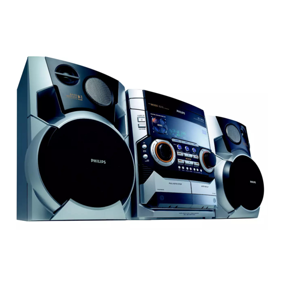
Mini System
Service
Service
Service
Service
Service
Service Manual
©
Copyright 2002 Philips Consumer Electronics B.V. Eindhoven, The Netherlands
All rights reserved. No part of this publication may be reproduced, stored in a retrieval system or
transmitted, in any form or by any means, electronic, mechanical, photocopying, or otherwise
without the prior permission of Philips.
Published by KC 0209 Service Audio
Version 1.0
TABLE OF CONTENTS
Location Of Pc Boards & Version variations ................ 1-2
Technical Specifications ............................................. 1-3
Measurement Setup .................................................... 1-4
Service Aids, Safety Instruction, etc. .......................... 1-5
Disassembly Instructions & Service positions .............. 2
Service Test Programs & DEMO mode ......................... 3
Set Block Diagram and Wiring diagram ......................... 4
Mains Board ................................................................... 5
Front Board .................................................................... 6
Vcd - Mpeg-01B Module ............................................. 8
Etf7 Tape Module ........................................................ 9
3CDC-LC-VCD Module ............................................... 10
Combi Board ................................................................ 11
Set Mechanical Exploded view & parts list ................. 12
Printed in The Netherlands
Subject to modification
FW-M355/
FW-V355/
COMPACT
MP3-CD PLAYBACK
DIGITAL AUDIO
Page
CLASS 1
GB
22/34/37
21M
3139 785 30029
Advertisement
Table of Contents

Related Manuals for Philips FW-M355


Summary of Contents for Philips FW-M355
- Page 1 LASER PRODUCT © Copyright 2002 Philips Consumer Electronics B.V. Eindhoven, The Netherlands All rights reserved. No part of this publication may be reproduced, stored in a retrieval system or transmitted, in any form or by any means, electronic, mechanical, photocopying, or otherwise without the prior permission of Philips.
-
Page 2: Mains Board
LOCATION OF PC BOARDS VERSION VARIATIONS: Type /Versions: FW-M355 FW-V355 Features & Board in used: Karaoke News Incredible Surround Rotary Encoder (volume control) Jog Shuttle Voltage Selector Aux / CDR Input Video Output Headphone Socket Line Output Subwoofer Output Surround Output... - Page 3 SPECIFICATIONS GENERAL: CASSETTE RECORDER: Mains voltage : 110-127V/220-240V Switchable for /21M Number of track : 2 x 2 stereo 220-230V for /22/34 Tape speed : 4.76 cm/sec +2.5/-1.5% 120V for /37 Wow and flutter : < 0.4% DIN Mains frequency : 50/60Hz Fast-wind/rewind time C60 : 130 sec...
-
Page 4: Measurement Setup
MEASUREMENT SETUP Tuner FM Bandpass LF Voltmeter 250Hz-15kHz e.g. PM2534 e.g. 7122 707 48001 RF Generator e.g. PM5326 S/N and distortion meter e.g. Sound Technology ST1700B Use a bandpass filter to eliminate hum (50Hz, 100Hz) and disturbance from the pilottone (19kHz, 38kHz). Tuner AM (MW,LW) Bandpass LF Voltmeter... -
Page 5: Service Aids
SERVICE AIDS Service Tools: ESD Equipment: Universal Torx driver holder ........4822 395 91019 Anti-static table mat - large 1200x650x1.25mm ... 4822 466 10953 Torx bit T10 150mm ..........4822 395 50456 Anti-static table mat - small 600x650x1.25mm ..4822 466 10958 Torx driver set T6 - T20 ......... -
Page 6: Laser Product
WAARSCHUWING WARNING Alle IC’s en vele andere halfgeleiders zijn All ICs and many other semi-conductors are gevoelig voor electrostatische ontladingen susceptible to electrostatic discharges (ESD). (ESD). Careless handling during repair can reduce life Onzorgvuldig behandelen tijdens reparatie kan drastically. de levensduur drastisch doen verminderen. When repairing, make sure that you are Zorg ervoor dat u tijdens reparatie via een connected with the same potential as the mass... -
Page 7: Front Board
DISMANTLING INSTRUCTIONS Dismantling of the Front Panel assembly Dismantling the 3CDC Module 1) Loosen the 4 screws, slide Cover top (pos 255) towards 4) Remove the Cover Tray (pos 106) as shown in figure 1. 1) Loosen 2 screws below the Front Panel (pos 101) mounting 4) Loosen 8 screws B to remove the Front board as shown in the rear and remove it upwards. - Page 8 Separating the MPEG and 3CDC-LC-VCD Module Dismantling of the Bottom & Rear Panel assembly Service pos B 1) Loosen 5 screws D mounting the Combi board to the Rear 1) Loosen 4 screws P to remove the MPEG shield & MPEG Board as shown in figure 9.
- Page 9 SERVICE TEST PROGRAM To start service test program hold P & TAPE depressed while plugging in the mains cord S refers to Service Mode. Display shows the ROM version * V refers to Version. "S-Vyy" (Main menu) yy refers to Software version number of Processor. (Counting up from 01 to 99) Mini 2002 FW-C1xx, C2xx, C3xx Dated: wk141 TUNER...
- Page 10 SET BLOCK DIAGRAM +12V_M 1.0 Vpp -6dB Track NOTE : +12V_A -CMOS (-9V) MAIN SIGNAL PATH SA BUFFER -33V -CMOS MPEG3 VCD-3C 500mV 250mV +12V_A 125mV MEASUREMENTS ARE IN AUX MODE : FM (67.5 kHz) 76dBA ECO6 +12V_A AM (80% MOD) 16dB XX mV LEVELS AT MAX VOL...
- Page 11 SET WIRING DIAGRAM 1805 CDC-L2C # VCD NON-VCD # 1801/1802 CD_LEFT CD_LEFT MIC_DET MIC_DET FRONT GND_A GND_A CD CHANGER +12V_A +12V_A CD_RIGHT CD_RIGHT MIC_SK MIC_SK +5V_CD +5V_CD GND_A GND_A (1101) GND_D GND_D MIC_VCD (1104) +12M +12M FFC SIDE CD_SWINFO CD_SWINFO CD_SHSTR CD_SHSTR MIC AMP...
- Page 12 COMPONENT LAYOUT This assembly drawing shows a summary of all possible versions. For components used in a specific version see schematic diagram and respective parts list. MAINS BOARD TABLE OF CONTENTS Component Layout ............5-1 Circuit Diagram ..............5-2 Electrical parts list ............5-3 3139 113 3465 pt 1 dd wk149 3230 is soldered manuall on the copper side for pt 1 pcb...
- Page 13 MAINS CIRCUIT 1201 A3 1207 C5 1211 E6 2203 A8 2207 A6 2211 B9 2215 B9 3205 A9 3209 B1 3216 B1 3221 A2 5206 C1 7201 A6 7205 B7 5201 A4 6204 A10 6208 A8 6212 B9 6216 B6 9202 C1 9206 E2 1204 C3...
- Page 14 ELECTRICAL PARTS LIST - MAINS BOARD MISCELLANEOUS 1201 4822 071 52001 Fuse T200mA 250V /22 3224 4822 053 21225 2M2 5% 0,5W 1204 2422 132 07519 Relay 1P 12V 16A 6204 4822 130 30621 1N4148 6205 4822 130 30621 1N4148 1205 9965 000 07788 Fuse T2A 250V /21M 6206 4822 130 31878...
- Page 15 FTD DISPLAY PIN CONNECTIONS FRONT BOARD Col 1 (12G) (11G) (2G - 9G) TABLE OF CONTENTS FTD Display pin connection ..........6-1 Variation Tables ............... 6-2 (Left) Circuit Diagram - Karaoke part ........6-3 j , p j , p j , p j , p j , p...
- Page 16 AUTO AUTO AUTO AUTO A55490 FW-V355/21M 1432 AUTO AUTO A55500 FW-C355/34 1433 NEWS RETURN NEWS NEWS NEWS A55520 FW-M355/22 1438 with LPC A55530 FW-M355/34 1439 without LPC A55540 FW-M355/37 1801 VCD & KARAOKE 1802 KARAOKE 3529 330R 330R 330R 330R...
- Page 17 CIRCUIT DIAGRAM - KARAOKE PART 1800 A1 2428 A8 2803 B3 2806 B5 2809 E3 2812 E5 2815 E7 2818 E7 3801 A2 3804 A4 3807 B4 3810 A5 3813 C7 3816 E4 3819 E5 3822 E7 5800 B2 7411 A9 7802 E2 7805 E7 1801 B9...
- Page 18 CIRCUIT DIAGRAM - MICROPROCESSOR PART 1400 A5 3472 B3 6415 E8 1402 F13 3473 B3 6416 E8 1406 D9 3474 B3 6417 F8 1407 D9 3475 B4 6422 A9 -FTD 1408 C9 3476 B4 6423 A9 1409 C9 3477 B4 6424 A11 1400 +5V6...
- Page 19 CIRCUIT DIAGRAM - HEADPHONE / MISCELLANEOUS PART 1438 A1 2400 F4 2404 B7 2408 B9 2412 B4 2416 A4 2420 A5 2424 F3 2600 D8 2606 F8 3402 B9 3408 F4 3413 A3 3417 C3 3421 C8 3567 B8 3601 E6 3605 F7 4406 F4 4410 B5...
-
Page 20: Component Layout
COMPONENT LAYOUT This assembly shows a summary of all possible versions. For components used in a specific version see schematics and respective parts list, 3139 113 3469pt 2 ... 90740 dd wk208... - Page 21 CHIP LAYOUT This assembly shows a summary of all possible versions. For components used in a specific version see schematics and respective parts list, 3139 113 3469pt 2 ... 90740 dd wk208...
- Page 22 ELECTRICAL PARTS LIST - FRONT BOARD ELECTRICAL PARTS LIST - FRONT BOARD MISCELLANEOUS 1400 3139 110 52850 FTD Display 12-ST-29GNK 2434 5322 126 11583 10nF 10% 50V 3414 4822 051 30102 1k 5% 0,062W 3471 4822 051 30102 1k 5% 0,062W 1402 4822 267 10953 Flex Socket 7pin Vert.
- Page 23 ELECTRICAL PARTS LIST - FRONT BOARD ELECTRICAL PARTS LIST - FRONT BOARD RESISTORS 3524 4822 116 52219 330R 5% 0,5W 3801 4822 117 11817 1k2 1% 1/16W 4437 4822 051 30008 0R Jumper 0603 4491 4822 051 30008 0R Jumper 0603 3525 4822 116 52219 330R 5% 0,5W 3802 4822 051 30103...
- Page 24 ELECTRICAL PARTS LIST - FRONT BOARD TRANSISTORS & INTEGRATED CIRCUITS 7400 3139 110 52961 TMP87CS71F “V355S52961” for FW-V355/21M 7400 3139 110 53141 TMP87CS71F “M355S53141” for FW-M355/22 7401 9352 679 67118 SAA6579T/V1/M4 7402 9322 155 82667 IR Reciver TSOP2236ZC1 7403 9965 000 04931 M24C01-WMN6...
-
Page 25: Vcd - Mpeg-01B Module
EXPLODED VIEW OF MODULE 3CDC-LC-VCD Module D3 x 16 VCD - MPEG-01B MODULE This chapter shows the MPEG-01B Board, for 3CDC-LC-VCD mechanism & electronics please refer to Chapter 10 Flex Cable 22pin TABLE OF CONTENTS (3139 110 35290) Plate Insulation CDC-LC Exploded View of Module .......... - Page 26 NOTES: Brief Introduction on the MPEG 1. When VCD source is selected the MPEG_RESET line will go positive triggering the following: DRST pulse to reset 8-bit microcontroller IC 7212 RSTOUT# pulse to reset IC 7201 ES3880 IC7212 sends CD10_RST to reset Signal Processor IC 7802 on the CD Board. 2.
- Page 27 MPEG-01B BLOCK DIAGRAM 8-BIT MICROCONTROLLER (IC 7212) INTERNAL BLOCK To Front Microprocessor via Servo Board Conn. MPEG-01B 1601 - DSA_ACK P2-0 P0-0 - DSA_DAT - DSA_STB P2-1 P0-1 P2-2 P0-2 P2-3 P0-3 DRAM MSM514265E P2-4 P0-4 P2-5 P0-5 +3.5V From MIC_IN P2-6 P0-6...
- Page 28 ES3880 VIDEO CD PROCESSOR CHIP VISBA VIDEO PC PROCESSOR CHIP PIN DESCRIPTION Name Number Definition 1, 31, 51 Voltage supply for 3.3 V. RAS# DRAM row address strobe (active low). LA12 AUX4 DWE# DRAM write enable (active low). LA13 AUX3 DA[8:0] 12:4 DRAM multiplexed row and column address bus.
- Page 29 ES3883 VIDEO CD COMPANION CHIP Name Number I/O Definition Transmit audio data input. TBCK Transmit audio bit clock. Dual-purpose pin RWS is the receive audio frame sync. 79 78 77 76 75 74 73 72 71 70 69 68 67 66 65 64 63 62 61 60 59 58 57 56 55 54 53 52 DSC_D7 MIC2 SEL_PLL1...
- Page 30 MPEG-01B BOARD LAYOUT 3139 113 3448 pt2 dd wk0141 3139 113 3448 pt2 dd wk0141...
- Page 31 ES3880 CIRCUIT 1601 D1 2210 E9 2258 E9 2271 E1 2276 C2 2280 C9 3204 C3 3207 C4 3210 E3 3214 B9 3234 E8 3272 B2 3275 B8 5207 E9 7201 B4 7205-A F2 7205-D F2 2201 E9 2223 A3 2268 D1 2272 F1 2277 B2...
- Page 32 ES3883 CIRCUIT 1602 C9 2213 D1 2216 D2 2219 C9 2225 B8 2228 A7 2231 B6 2253 A1 2259 E7 2263 C7 2284 A4 3219 E2 3224 B4 3227 F8 3231 E8 3235 D9 3238 F7 3241 F1 3244 D8 3247 B8 3250 B7 4001 F3...
- Page 33 AUDIO CIRCUIT 2202 F3 2203 F3 2204 F3 2209 F1 2212 F2 2251 2221 F6 2237 D1 2238 F7 3266 2240 D1 2242 C3 2243 F5 2244 D2 2245 C1 AGND 4u7 2260 3265 2246 C1 2.4V AOL- 2249 F2 2252 10u 3285 LEFT...
- Page 34 8-10 8-10 ELECTRICAL PARTS LIST - MPEG-01B BOARD ELECTRICAL PARTS LIST - MPEG-01B BOARD MISCELLANEOUS 5207 4822 526 10704 FE Bead 100MHz 1601 2422 025 16837 Flex Socket 22pin Hort. 2266 3198 016 31020 1nF 5% 25V 3243 4822 051 30472 4k7 5% 0,062W 5208 4822 526 10704...
-
Page 35: Etf7 Tape Module
Tapedeck wiring (Double deck) TO ETF BOARD CONNECTOR 1770 (ND) 14P CONNECTOR 1740 (DB) 14P CRO2* CRO2* * Not for Ferro version ETF7 TAPE MODULE (Non-Dolby Version) MODE TAPE DECK MOTOR Mechanism B Mechanism A TO ETF BOARD TO ETF BOARD CONNECTOR 1730 (3P) CONNECTOR 1710 (ND) 5P CONNECTOR 1720 (DB) 6P... - Page 36 BLOCK DIAGRAM Line-In ATTEN 7710 7720 PB Out 9792 # Playback SOURCE SEL PRE-AMPLIFIER ATTEN Head AN7318S HEF4952BT For Dolby version only ALCEN 1A0 1A1 1A2 PB In PB Out 7630 Rec current REC Out DOLBY B NR Rec/Pb 7740 Rec In CXA1101M Head...
- Page 37 Brief introduction General Playback Mode 13. Motor Speed (For FR versions only) During High speed dubbing, a feedback signal from the uP through pin 03 of the IC7610 (HEF4094BT) will trigger the Signal from the playback head Deck A or Deck B is selected and fed through by the Mode Selector IC7710 (HEF4952BT). transistors 7622 (BC847B) and 7616 (BC857B) to cause a change in the voltage level between High and Low, thus changing The signal is amplified by amplifier IC7720 (AN7323S) before feeding to the IC7740 (HEF4952BT) and out to the AF Board the speed of the motor.
- Page 38 CONNECTORS ASSIGNMENTS: CONNECTOR 1701 INTERCONNECTION TO AF BOARD CONNECTOR 1740 DECK A & B CONTROL INTERFACE (For Dolby B NR version only) REC-L Record input left REC REW Record tab protection status switch (reverse) [open=on: close=off] REC-R Record input right CrO2 B Chrome tape detection switch deck B [open=Cr: close=Fe]...
- Page 39 TAPE MECHANISM ELECTRONICS TAPE ADJUSTMENT & CHECK TABLE TEST ADJUST RECORDER MEASURE READ ON CASSETTE MODE with B Photo Sensor 1. B Rec Switch (REV) Rec-R ADJUST MOTOR SPEED 2. B CrO2 Switch CrO2* PLAY B 3620 3150Hz +/- 0.5% SBC420 frequency NORMAL SPEED...
- Page 40 COMPONENT LAYOUT CHIP LAYOUT Some location on this board is prepared for both 0603 & 0805 SMDs footprint, 3139 113 3409 pt2 dd wk0042 in such locations 0603 SMDs may be substituted. 3139 113 3409 pt2 dd wk0042...
- Page 41 ANALOG CIRCUIT 1701 F9 2705 A2 2712 B6 2719 C5 2726 D4 2735 B3 2745 F5 2765 B4 2785 F1 3705 A4 3712 B4 3719 C6 3726 D5 3733 A2 3744 F8 3753 F5 3760 A7 3767 A7 3774 E3 3781 D2 4794 C6 6774 D3...
- Page 42 SERVO CONTROL CIRCUIT 1702 A7 1760 B8 2622 D2 2625 E4 3601 B2 3604 C2 3607 C6 3610 D6 3613 B2 3618 A4 3622 A4 3625 B3 3630 A6 3676 C5 3680 C5 3687 D2 4785 D2 6612 B6 7612 A6 7616 A4 7620 B6 7624 D6...
- Page 43 TAPE MECHANISM - MOTOR EXPLODED VIEW TAPE MODULE EXPLODED VIEW 4822 361 11055 Motor Assembly 1 3139 118 77130 Autoreverse Mech. CWE44FR01 Screw M2,6 x 5 1 3139 118 77140 Non-Autoreverse Mech. CWE44FF02 Chrome/Ferro Screw M2 x 5 1 3139 118 77950 Non-Autoreverse Mech.
- Page 44 9-10 9-10 TAPE MECHANISM A - PLAY MECHANICAL PARTS - PLAY MECHANISM 9965 000 02313 Play Head (Non-Autoreverse deck) 9965 000 02321 Play Head (Autoreverse deck) 4822 402 10972 Pinch Arm Assembly R 9965 000 02314 Coil Assembly 9965 000 06443 Cam Gear 4822 528 11209 Flywheel Assembly RV...
- Page 45 9-11 9-11 TAPE MECHANISM B - RECORD/PLAYBACK (Non-Autoreverse version) MECHANICAL PARTS - REC/PB MECHANISM 9965 000 02313 Play Head 9965 000 02600 Head, Erase 4822 402 10972 Pinch Arm Assembly R 9965 000 02314 Coil Assembly 9965 000 06443 Cam Gear 4822 528 11209 Flywheel Assembly RV 44-2...
- Page 46 9-12 9-12 TAPE MECHANISM B - RECORD/PLAYBACK (Autoreverse version) MECHANICAL PARTS - REC/PB MECHANISM 4822 402 10972 Pinch Arm Assembly R 9965 000 02314 Coil Assembly 9965 000 06443 Cam Gear 4822 528 11209 Flywheel Assembly RV 9965 000 02322 Belt AF 44-2 9965 000 02317...
- Page 47 9-13 9-13 ELECTRICAL PARTS LIST - ETF7 NON-DOLBY BOARD ELECTRICAL PARTS LIST - ETF7 NON-DOLBY BOARD MISCELLANEOUS 2738 482212614585 100nF 10% 50V 3685 482211652234 100k 5% 0,5W 3745 482205120332 3k3 5% 0,1W Autoreverse 1701 482226710953 Flex Socket 7pin Vert. 2741 482212611585 22nF +80/-20% 25V 3686 482211710837 100k 1% 0,1W...
- Page 48 9-14 9-14 ELECTRICAL PARTS LIST - ETF7 NON-DOLBY BOARD RESISTORS 4706 482205120008 0R Jumper 0805 6612 482213031878 1N4003G 4707 482205120008 0R Jumper 0805 6614 482213030621 1N4148 Autoreverse 4708 482205120008 0R Jumper 0805 6770 482213030621 1N4148 4709 482205120008 0R Jumper 0805 6771 482213030621 1N4148 4710 482205120008...
- Page 49 10-2 10-1 Service hints CAUTION CHARGED CAPACITORS ON THE SERVO BOARD MAY DAMAGE THE CD DRIVE ELECTRONICS WHEN CONNECTING A NEW CD MECHANISM. THAT´S WHY, BESIDES THE SAFETY MEASURES LIKE • SWITCH OFF POWER SUPPLY • ESD PROTECTION ADDITIONAL ACTIONS MUST BE TAKEN BY THE REPAIR TECHNICIAN. The following steps have to be done when replacing the CD mechanism: 1.
- Page 50 10-3 10-4 Service hints Wiring Dismantling of Tray 1. Open the tray. 2. Release 2x catch as shown in fig. 2 and Disc Motor Detail A 3. Pull tray out. Inner switch Detail A Slide Motor fig.2 Assembling of Tray Service Position 1.
- Page 51 10-5 10-5 BLOCK DIAGRAM 3CDC-LC VCD Version CD MECHANISM MAINBOARD VAM2201 DISC 7816 1805 M63000 7803 7802 EXCK DQSY DQSY TURNTABLE SBSO FOCB+ MOTOR CD Text FOCUS SBSY SCOR SRDT SRDT MOTOR SFSY WFCK µP_CLK FOCB- SCLK CL11 CD Text LC89170M 1802 RADIAL...
- Page 52 10-6 10-6 Mapping Copperside Componentside 2800 F4 3732 C2 3851 E4 4828 C3 7823 F2 0801 E2 2801 D4 3733 C2 3852 F1 4829 G4 0802 C3 3CDC-LC (Herman) Copperside view 2802 E4 3734 D2 3853 E4 4830 G3 0803 A4 3CDC-LC (Herman) Components seen from Copperside 2803 D4 3735 G2...
- Page 53 10-7 10-7 1800 2803 2808 2815 2830 2839 2848 2886 3704 3722 3728 3802 3808 3822 3834 3839 3845 3852 3866 3874 7801 7822 1801 2804 2809 2817 2831 2840 2859 2887 3709 3724 3729 3803 3811 3824 3835 3841 3846 3854 3868...
- Page 54 10-8 10-8 Mapping Copperside Componentside 2800 F4 3732 C2 3851 E4 4828 C3 7823 F2 0801 E2 2801 D4 3733 C2 3852 F1 4829 G4 0802 C3 3CDC-LC (Herman) Copperside view 2802 E4 3734 D2 3853 E4 4830 G3 0803 A4 3CDC-LC (Herman) Components seen from Copperside 2803 D4 3735 G2...
- Page 55 10-9 10-9 1802 2816 2823 2833 2843 2870 3705 3712 3718 3733 3767 3804 3812 3817 3825 3832 3858 3862 3878 6807 7802 1805 2818 2824 2834 2845 2871 3706 3712 3730 3734 3769 3808 3813 3818 3826 3849 3859 3864 3881 6809...
- Page 56 10-10 10-10 1875 1876 1880 1883 2878 3714 3745 3754 3771 6801 6808 8003 Drawer bottom view 1875 1876 1881 2860 2881 3715 3747 3755 3772 6802 7812 1875 1876 1882 2872 2883 3719 3748 3765 3773 6803 7813 1875 1877 1882 2873...
- Page 57 10-11 10-11 EXPLODED VIEW (3CDC-LC M ODULE MECHANICAL PARTS Drawer → Chapter 10-10 ––––––––––––––––––––––––––––––––––––––––––––––––––––– 3103 304 66500 DRAWER 3103 304 66490 CAROUSEL 3103 304 06860 PULLEY DRAWER 45 5x 3103 304 06850 ECCENTRIC GEAR WHEEL 3103 304 06980 NAIL FIXATION 3103 304 66850 DRIVING BELT CAROUSEL 4822 532 12365 BUSH DRAWER (height=5,5mm,d=9,4mm) 3103 304 66550 BRACKET-DISC...
- Page 58 10-12 10-12 ELECTRICAL PARTSLIST 3CDC-LC-VCD MODULE ELECTRICAL PARTSLIST 3CDC-LC-VCD MODULE –––––––––––––––––––––––––––––––––––––––––––––––––––––––––––––––––––––––––––––––––––––––––––––––––––––––––––––––––– –––––––––––––––––––––––––––––––––––––––––––––––––––––––––––––––––––––––––––––––––––––––––––––––––––––––––––––––––– MISCELLANEOUS CAPACITORS RESISTORS RESISTORS ––––––––––––––––––––––––––––––––––––––––––––––––––––– ––––––––––––––––––––––––––––––––––––––––––––––––––––– ––––––––––––––––––––––––––––––––––––––––––––––––––––– ––––––––––––––––––––––––––––––––––––––––––––––––––––– 9305 022 30107 CD Drive VAM2201/07 2877 © 4822 126 14226 82pF 3810 © 4822 051 30471 470Ω 0,06W 4728 © 4822 051 20008 CHIP JUMPER 0805 4822 361 10753 CAROUSEL MOTOR...
- Page 59 10-14 10-13 Technical remarks ELECTRICAL PARTSLIST 3CDC-LC-VCD MODULE –––––––––––––––––––––––––––––––––––––––––––––––––––––––––––––––––––––––––––––––––––––––––––––––––––––––––––––––––– RESISTORS TRANSISTORS ––––––––––––––––––––––––––––––––––––––––––––––––––––– ––––––––––––––––––––––––––––––––––––––––––––––––––––– 4868 © 4822 051 20008 CHIP JUMPER 0805 7806 © 4822 130 60511 BC847B 4869 © 4822 051 20008 CHIP JUMPER 0805 7812 © 4822 130 60511 BC847B 4870 ©...
-
Page 60: Combi Board
11-1 11-1 Brief introduction of the Combi Board A. TRANSFORMER PRIMARY PART Transformer Primary Circuit provide connection for AC mains supply and primary wires of transformer. B. POWER SUPPLY PART Power Supply Circuit consists of rectifiers, capacitive filters and voltage regulators. Regulated voltage include +5V6, +LED, +12A, +12M, -32V, PWDN. - Page 61 11-2 11-2 CHIP LAYOUT - MAIN PART (excluding the Tuner portion) This assembly drawing shows a summary of all possible versions. For components used in a specific version see schematic and respective parts list. For Information on this Tuner portion please refer: Page 11-8 for Non-Cenelec Tuner Page 11-10 for Cenelec Tuner 3139 118 3462pt2 / 3463pt2 ...90280 dd wk151...
- Page 62 11-3 11-3 COMPONENT LAYOUT - MAIN PART (excluding the Tuner portion) This assembly drawing shows a summary of all possible versions. For components used in a specific version see schematic and respective parts list. For Information on this Tuner portion please refer: Page 11-8 for Non-Cenelec Tuner Page 11-10 for Cenelec Tuner 3139 118 3462pt2 / 3463pt2 ...90280 dd wk151...
- Page 63 11-4 11-4 CHIP LAYOUT - MAIN PART (excluding the Tuner portion) This assembly drawing shows a summary of all possible versions. For components used in a specific version see schematic and respective parts list. For Information on this Tuner portion please refer: Page 11-10 for Non-Cenelec Tuner Page 11-12 for Cenelec Tuner 3139 118 3462pt3 / 3463pt3 ...90280 dd wk209...
- Page 64 11-5 11-5 COMPONENT LAYOUT - MAIN PART (excluding the Tuner portion) This assembly drawing shows a summary of all possible versions. For components used in a specific version see schematic and respective parts list. For Information on this Tuner portion please refer: Page 11-10 for Non-Cenelec Tuner Page 11-12 for Cenelec Tuner 3139 118 3462pt3 / 3463pt3 ...90280 dd wk209...
- Page 65 11-6 11-6 POWER SUPPLY CIRCUIT 85 D1 3250 F5 7219 F4 86 D1 3251 D7 7220 E5 87 E1 3252 D4 7504 E6 88 E1 3253 D4 9222 A2 1209 B2 3254 D4 9223 A2 9296 for /21/22 7210 1214 A3 3570 F6 9224 B6 7211...
- Page 66 11-7 11-7 SOURCE SELECTION CIRCUIT C3 E15 C10 C14 1501 D1 1507 C13 2504 B4 2510 D4 2516 G8 2522 G7 2528 F7 2534 H10 2540 G11 2549 E15 2568 D15 3563 E12 9602 D15 2665 G5 3505 B3 3511 D3 3517 E2 3523 C6 3534 H9...
- Page 67 11-8 11-8 PRE- & POWER AMPLIFIER CIRCUIT 0888 E13 1323 E14 2365 E12 2370 F13 2378 E12 2608 D2 2613 G1 2618 E4 3356 E14 3361 E7 3366 F12 3371 E12 3377 B10 3386 C13 3392 C8 3612 D4 3617 B5 3622 G1 3627 E4 3632 A1...
- Page 68 11-9 11-9 TRANSFORMER PRIMARY PART - CIRCUIT & LAYOUT TRANSFORMER SECONDARY PART - CIRCUIT VIDEO OUT PART - CIRCUIT & LAYOUT (except /21/22 version) & LAYOUT (except /21/22 version) (for VCD version only) 1 F4 3 E4 5 D4 7 C4 1202 D1 5202 C2 9201 C2...
- Page 69 11-10 11-10 NON-CENELEC TUNER PORTION - COMPONENT & CHIP LAYOUTS TUNER ADJUSTMENT TABLE ( ECO6 FM/MW- and FM/MW/LW - versions with AM-frame aerial ) Waverange Input frequency Input Tuned to Adjust Output Scope/Voltmeter VARICAP ALIGNMENT 8V ±0.2V 108MHz 5130 This assembly drawing shows a summary of all possible versions. For components 87.5 - 108MHz 4.3V ±0.5V 87.5MHz...
- Page 70 11-11 11-11 NON-CENELEC TUNER CIRCUIT c1 E14 5119 G9 c2 F14 5121 E11 c3 F14 5123 G5 c4 F14 5130 E5 TUNER BOARD ECO6 / SYSTEMS NON CENELEC c5 F14 5131 C6 c6 F14 6103 B2 c8 F14 6105-1 F3 1101 2105 USA c9 F14...
- Page 71 11-12 11-12 CENELEC TUNER PORTION - COMPONENT & CHIP LAYOUTS TUNER ADJUSTMENT TABLE ( ECO6 Cenelec FM/MW - and FM/MW/LW - versions with AM-frame aerial ) Waverange Input frequency Input Tuned to Adjust Output Scope/Voltmeter VARICAP ALIGNMENT 8V ±1.2V 108MHz check 87.5 - 108MHz This assembly drawing shows a summary of all possible versions.
- Page 72 11-13 11-13 CENELEC TUNER CIRCUIT AM G13 5118 G9 FM G13 5119 G9 1101 A2 5121 E11 1102 B1 5122 H5 TUNER BOARD ECO6 1103 E2 5123 G5 / SYSTEMS-CENELEC VERSION PROGRAMMING COMPONENTS 1110 B2 6105-1 E4 1130 A2 6105-2 G6 AM-IF1 1131 C1 6106 D4...
- Page 73 11-14 11-14 ELECTRICAL PARTS LIST - COMBI BOARD (excluding Tuner portion) ELECTRICAL PARTS LIST - COMBI BOARD (excluding Tuner portion) MISCELLANEOUS 1214 4822 071 55002 Fuse T5A 250V /34/37 2373 4822 122 33777 47pF 5% 63V 2604 2020 552 94427 100pF 5% 50V 3250 4822 051 30472...
- Page 74 11-15 11-15 ELECTRICAL PARTS LIST - COMBI BOARD (excluding Tuner portion) ELECTRICAL PARTS LIST - COMBI BOARD (excluding Tuner portion) RESISTORS 3531 4822 117 12925 47k 1% 0,063W 4514 4822 051 30008 0R Jumper 0603 4576 4822 051 30008 0R Jumper 0603 3532 4822 117 12925 47k 1% 0,063W...
- Page 75 11-16 11-16 ELECTRICAL PARTS LIST - COMBI BOARD (Non-Cenelec Tuner portion only) ELECTRICAL PARTS LIST - COMBI BOARD (Non-Cenelec Tuner portion only) RESISTORS MISCELLANEOUS 3101 4822 051 30333 33k 5% 0,062W 6107 9340 386 90115 BZX284-C11 1101 2422 015 19376 Socket 2P Clickfit USA only 3102...
- Page 76 11-17 11-18 ELECTRICAL PARTS LIST - COMBI BOARD (Cenelec Tuner portion only) ELECTRICAL PARTS LIST - COMBI BOARD (Cenelec Tuner portion only) DIODES MISCELLANEOUS 6107 9340 386 90115 BZX284-C11 1102 4822 267 10283 Socket Coaxial 75R 3142 4822 100 12159 Trimpot 100k 30% 1103 4822 265 31184...
- Page 77 12-1 12-1 EXPLODED VIEW - MAIN UNIT 1102C Blown-up of the Heaksink area Exploded view 3139 119 34330 dd wk208...
- Page 78 9965 000 11602 Right LS Box FW-V355/21M M3 x 10 3139 118 18350 Window Display /21M 9965 000 11651 Left LS Box FW-M355/22/34 M3 x 10 3139 118 18140 Window Display /22 9965 000 11652 Right LS Box FW-M355/22/34 M3 x 10...
Need help?
Do you have a question about the FW-M355 and is the answer not in the manual?
Questions and answers