Radio Shack TRS-80 Model 4 Technical Reference Manual
Microcomputer
Hide thumbs
Also See for TRS-80 Model 4:
- Introduction manual (42 pages) ,
- Technical reference manual (408 pages) ,
- Owner's manual (418 pages)
Table of Contents
Advertisement
Quick Links
Advertisement
Table of Contents

Subscribe to Our Youtube Channel
Related Manuals for Radio Shack TRS-80 Model 4


Summary of Contents for Radio Shack TRS-80 Model 4
-
Page 3: Limited Warranty
No action arising out of any claimed breach of this Warranty or transactions under this Warranty may be brought more than two (2) years after the cause of action has accrued or more than four (4) years after the date of the Radio Shack sales document for the Equipment or Software, whichever first occurs. -
Page 5: Reference Manual
® TRS-80 MODEL 4 TECHNICAL REFERENCE MANUAL A DIVISION OF TANDY CORPORATION FORT WORTH, TEXAS 76102... - Page 6 ® TRSDOS Version 6 Operating System: © 1983 Logical Systems. Licensed to Tandy Corporation. All Rights Reserved. Model 4 Technical Reference Manual; Hardware Part: © 1983 Tandy Corporation. All Rights Reserved. Model 4 Technical Reference Manual; Software Part: © 1983 Tandy Corporation and Logical Systems. All Rights Reserved.
-
Page 7: Important Notice
TRS-80 Model 4 operation. Radio Shack will not be liable for any damage caused, or alleged to be caused, by the customer or any other person using this technical manual to repair, modify, or alter the TRS-80 Model 4 Computer in any manner. -
Page 9: Table Of Contents
TABLE OF CONTENTS Part 1 / Hardware SECTION I Introduction.............................1 SYSTEM OVERVIEW ........................3 BLOCK DIAGRAM..........................3 JUMPER OPTIONS..........................5 SECTION II Disassembly / Assembly........................7 Disassembly .............................9 2.1.1 Case ..............................9 2.1.2 CPU Board............................9 2.1.3 FDC Board (optional)........................9 2.1.4 RS-232 Board (optional) ........................9 2.1.5 Main Power Supplies ........................9 2.1.6 Disk Drives (optional)........................9... - Page 10 4.1.2 Nonmaskable Interrupt Logic......................55 4.1.3 Drive Select Latch and Motor On Logic ..................55 4.1.4 Wait State Generation and WAITIMOUT Logic ................56 4.1.5 Clock Generation Logic ......................... 56 4.1.6 Disk Bus Selector Logic ......................... 56 4.1.7 Read/Write Data Pulse Shaping Logic ..................56 4.1.8 Disk Bus Output Drivers ........................
-
Page 11: List Of Figures
LIST OF FIGURES Fig. No. Description Page No. TRS-80 Model 4 Interconnection Diagram Model 4 Block Diagram RAM Memory Timing of U3 & CPU Timing of U4 CPU Video Access Timing I/O Bus Timing Diagram Write Precompensation Timing... -
Page 13: Part 1 / Hardware
PART I HARDWARE SECTION I INTRODUCTION... -
Page 15: System Overview
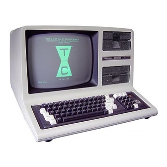
The Radio Shack TRS-80 Model 4 Microcomputer is an enhanced version of Radio Shack’s popular TRS-80 Model Ill Microcomputer. The TRS-80 Model 4 is software compatible with the Model Ill so that owners of either system can take advantage of the large number of programs available. - Page 16 FIGURE 1-1. TRS-80 MODEL 4 INTERCONNECTION DIAGRAM...
-
Page 17: Jumper Options
1.3 JUMPER OPTIONS 1.3.1 16K to 64K 1. Remove U77-U84 2. Move E5-E6 to E5-E4 Move E1-E2 to E2-E3 Move E12-E13 to E12-E11 3. Add E7-E8 and eight Tandy #8040665 ICs in locations U77-U84. 4. Remove capacitors 068, 072, 076, 080, 084, 088, 092 and 096. -
Page 19: Disassembly / Assembly
SECTION II DISASSEMBLY / ASSEMBLY... -
Page 21: Disassembly
DISASSEMBLY / ASSEMBLY 2.1.4 RS-232 Board (optional) 2.1 Disassembly NOTE: The CPU Board must be removed before 2.1.1 Case removing the RS-232 Board. 1. Remove all cables from the bottom and rear of 1. Be sure to remove all cables connecting the RS- the Computer. -
Page 22: Video Monitor (Crt) And Video Board
2. Remove the four screws and washers (two on WARNING each side) which connect the Drive to the Disk There may be a high voltage charge on the high Mounting Bracket. Remove the RFI shield which voltage anode. To discharge, connect one end of a covers the top drive. -
Page 23: Assembly
2.2.6 Disk Drive Power Supply (optional) 2.2 Assembly 1. Before installing the Power Supply be sure that 2.2.1 RS-232 Board (optional) the bottom Disk Drive is mounted in place and 1. Install the PC Board using #6 x 1/4” screws. If the Disk Shield is in position on the Disk applicable, press the PC Board onto the plastic Mounting Bracket. -
Page 25: Cpu Circuit Board
SECTION III CPU CIRCUIT BOARD... -
Page 27: Model 4 Theory Of Operation
3.1 Model 4 Theory of Operation 3.1.1 Introduction The TRS-80 Model 4 Microcomputer is a self-contained U19, U20, U31, and U32, this chip provides the wait cir- desktop microcomputer designed not only to be cuitry necessary to prevent the CPU from accessing completely software compatible with the TRS-80 Model video RAM during the active portion of the display. - Page 28 FIGURE 3-1. MODEL 4 BLOCK DIAGRAM...
- Page 29 FDC Status Reg. FDC Command Reg. EC - EF Resets RTC Int. Mode Output latch Rcvr Holding Reg. Xmit Holding Reg. UART Status Reg. UART/Modem control -reserved- Baud Rate Register Modem Status Master Reset/Enable UART control reg. E4 - E7 Read NMI Status Write NMI Mask reg.
- Page 30 Following is a Bit Map of the appropriate ports in the Model 4. Note that this is an “internal” bit map only. For bit maps of the optional devices, refer to the appropriate section of the desired manual. Model 4 Port Bit Map Port FC-FF Cass...
-
Page 31: Rom
3C00 - 3FFF Video RAM 4000 - 7FFF RAM (16K) End of one 32K Bank 8000 - FFFF RAM (32K) Second 32K Bank Memory Map III 0000 - 7FFF RAM (32K) End of One 32K Bank RAM (29K) Second 32K Bank 8000 - F3FF Keyboard F400 - F7FF... - Page 32 FIGURE 3-2. RAM MEMORY...
-
Page 33: Real Time Clock
3.1.9 Real Time Clock 3.1.11 Printer Circuitry The Real Time Clock circuit in the Model 4 provides a The printer status lines are read by the CPU by 30 Hz (in the 2 MHz CPU Mode) or 60 Hz (in the 4 enabling buffer U67. - Page 34 COMPONENT LOCATION / CIRCUIT TRACE, SOUND BOARD #8858121 SCHEMATIC 8000188, SOUND BOARD #8858121...
- Page 35 FIGURE 3-3. TIMING OF U3 & CPU...
- Page 36 FIGURE 3-4. TIMING OF U4...
- Page 37 FIGURE 3-5. CPU VIDEO ACCESS TIMING...
-
Page 38: Model 4 I/O Bus
See Model 4 Port Bit assignment for port 0FE, 0EC, 3.2 Model 4 I/O Bus and 0E0 on pages 28 and 29. The Model 4 Bus is designed to allow easy and The Model 4 CPU board is fully protected from convenient interfacing of I/O devices to the Model 4. - Page 39 Input or Output Cycles ∞ ∞ ∞ ∞ Inserted by Z80 CPU Input or Output Cycles with Wait States. ∞ ∞ ∞ ∞ Inserted by Z80 CPU †Coincident with IORQ* only on INPUT cycle FIGURE 3-6. I/O BUS TIMING DIAGRAM...
-
Page 40: Model 4 Port Bits
3.3 Model 4 Port Bits Name: WRNMIMASKREG* Name: RDINTSTATUS* Port Address: 0E4H Port Address: 0E0H Access: WRITE ONLY Access: READ ONLY Bit 7 = ENINTRO; 0 disables Disk INTRQ from NOTE: A 0 indicates the device is interrupting. generating an NMI. 1 enables above. - Page 41 Name: WRINTMASKREG* Name: DRVSEL* Port Address: 0E0H Port Address: 0F4H Access: WRITE ONLY Access: WRITE ONLY Bit 7 = Undefined Bit 7 = FM*/MFM; 0 selects single density, 1 selects double density. Bit 6 = ENERRORINT; 1 enables RS-232 interrupts on parity error, framing error, or data overrun Bit 6 = WSGEN;...
-
Page 43: Schematic 8000173, 64K Version Cpu Pcb 8858090
SCHEMATIC 8000173, 64K VERSION CPU PCB 8858090... -
Page 55: Cpu Component Layout
CPU COMPONENT LAYOUT... -
Page 57: Parts List, Cpu Pcb #6700104Aa3
Parts List, CPU PCB #6700104AA3 Model 4 16K, Cassette Input Catalog number 26-1067 Item Description Mfgr’s Part No. Cap, 100 pfd 50V C. Disk (C1,99,101,103) 8301104 Cap, 10 ufd 35V Elec. Rad (C2-4) 8326103 Cap, 0.1 ufd 50v Mono Axial 8374104 (C5,11-18,23,26-29,31,33-37,39-41,43,47-55, 57-97) - Page 58 Parts List, CPU PCB #6700104AA3 Model 4 16K, Cassette Input Catalog number 26-1067 Item Description Mfgr’s Part No. IC, 74LS373 Octal Latch (U7) 8020373 IC, 74LS273 Octal Flip-Flop (U8,37) 8020273 IC, 74LS153 Dual Multiplexer (U9) 8020153 IC, 74LS166 Shift Register (Ull) 8020166 IC, 74LS51 AND OR Invert (U12,20) 8020051...
- Page 59 Parts List, CPU PCB #6700104AA3 Model 4 16K, Cassette Input Catalog number 26-1067 Item Description Mfgr’s Part No. Relay, 12V 2 AMP (K1) 8429105 Res, 510 ohm, 5% 1/4W (R1,59) 8207151 Res, 12K ohm, 5% 1/4w (R2) 8207312 Res, 6.2K ohm, 1/4W (R3) 8207262 Res, 470 ohm, 5% 1/4w (R4,23) 8207147...
- Page 60 Parts List, CPU PCB #6700104AA3 Model 4 16K, Cassette Input Catalog number 26-1067 Item Description Mfgr’s Part No. Jumper Wire 20 Gauge (W1-3) *NOTE PCB Logic Board, Rev. PP3 8709296 Regulator, 79LO5, -5V (Q5) 8051905 Socket, 20-Pin DIP (U3,4,58,59,71-73) 8509009 Socket, 24-Pin DIP (U21,23,68-70) 8509001 Socket, 40-Pin DIP (U47,57)
-
Page 61: Parts List, Cpu Pcb 8858090
Parts List, CPU PCB 8858090 Model 4 64K, Single or Double Drive Catalog Number 26-1068 or 26-1069 Item Description Mfgr’s Part No. Cap, 100 pfd 50V C. Disk (C1,99,101,103) 8301104 Cap, 10 MFD 35V ELEC. RAD (C2-4) 8326103 Cap, 0.1MFD 50V MONO AXIAL 8374104 (C5,11-18,23,26-29,31,33-37,39-41,43, 47-55,57-65,67,69,71,73,75,77,79,81,83,... - Page 62 Parts List, CPU PCB 8858090 Model 4 64K, Single or Double Drive Catalog Number 26-1068 or 26-1069 Item Description Mfgr’s Part No. IC, 74LS166 Shift Register (Ull) 8020166 IC, 74LS51 AND OR Invert (U12,20) 8020051 IC, 74LS00 Quad 2-In NAND (U13,14) 8020000 IC, LM339 Comparator (U15) 8050339...
- Page 63 Parts List, CPU PCB 8858090 Model 4 64K, Single or Double Drive Catalog Number 26-1068 or 26-1069 Item Description Mfgr’s Part No. Res, 10K ohm, 5% 1/4w (R5,9,14,16) 8207310 Res, 3.6K ohm, 5% 1/4W (R6) 8207236 Res, 91 ohm, 5% (R7) 8207091 Res, 4.7K ohm, 5% 1/4W 8207247...
-
Page 65: Floppy Disk Interface
SECTION IV FLOPPY DISK INTERFACE... -
Page 67: Model 4 Fdc Pcb #8858060
4.1 Model 4 FDC PCB #8858060 interrupt to the CPU. The NMI-interrupt conditions are The TRS-80 Model 4 Floppy Disk interface Board is programmed by doing an OUT instruction to port E4H an optional board which if incorporated provides a with the appropriate bits set. -
Page 68: Wait State Generation And Waitimout Logic
4.1.4 Wait State Generation and WAITIMOUT Drive 2 or Drive 3 is selected, U17 pin 1will go low Logic indicating that an external drive is selected. One half of U10 (a five input NOR gate) is used to detect when As previously mentioned, a wait state to the CPU can one of the four drives is selected. -
Page 69: Floppy Disk Controller Chip
02 is used as the write data pulse on nominal 4.1.11 Adjustments and Jumper Options (EARLY = 0 LATE = 0). 01 is used for the early, and The Data Separator must be adjusted with the 1793 03 is used for the late. The leading edge of 04 resets in an idle condition (no command currently in the STB line in anticipation of the next write data operation). -
Page 70: Fdc Board To Cpu Board Signal Description
FLOPPY DISK CONTROLLER INTERFACE CONECTOR FDC BOARD TO CPU BOARD SIGNAL DESCRIPTION... -
Page 71: Schematic 8000095, Pcb Controller #8858060
SCHEMATIC 8000095E, FLOPPY DISK CONTROLLER #8858060... -
Page 73: Parts List, Fdc Pcb #8858060
PARTS LIST, FLOPPY DISK INTERFACE PC BOARD #8858060 MANUFACTURER’S RADIO SHACK SYMBOL DESCRIPTION PART NUMBER PART NUMBER CAPACITORS 0.lµF, 50V, monolithic, radial 838-4104 ACC104QJAP 0.lµF, 50V, monolithic, radial 838-4104 ACC104QJAP 0.lµF, 50V, monolithic, radial 838-4104 ACC104QJAP 0.lµF, 50V, monolithic, radial... - Page 74 PARTS LIST, FLOPPY DISK INTERFACE PC BOARD #8858060 MANUFACTURER’S RADIO SHACK SYMBOL DESCRIPTION PART NUMBER PART NUMBER INTEGRATED CIRCUITS (cont’d) 74LS174, Quad “D” Flip-Flop 802-0174 AMX3565 WD1793 850-9002 AXX3041 74LS38. NAND Buffer 802-0038 AMX4328 7416, Hex Inverter/Buffer 800-0016 ------- 74LS260, Dual NOR gate...
-
Page 75: Model 4 Fdc Pcb #8858160
CPU to check the FDC board to determine the source 4.2 Model 4 FDC PCB #8858160 of the non-maskable interrupt. Data bit 7 indicates the The TRS-80 Model III/4 Floppy Disk Interface Board status of FDC interrupt request (0 = true, 1 = false). is an optional board which, if incorporated, provides a Data bit 6 indicates the status of Motor Time Out (0 standard 5-1/4”... -
Page 76: Clock Generation Logic
perform this function. INTQ, DRQ, RESET, and are selected, otherwise the internal inputs are WAITIMOUT are the inputs to the NOR gate. If any selected. This control signal EXTSEL* is generated one of these inputs is active (logic high), the output of from the outputs of the Drive Select Latch. - Page 77 FIGURE 4-1. WRITE PRECOMPENSATION TIMING...
-
Page 78: Clock And Read Data Recovery Logic
4.2.9 Clock and Read Data Recovery Logic 4.2.10 Floppy Disk Controller Chip The Clock and Read Data Recovery Logic is The 1793 is an MOS LSI device which performs the comprised of one chip, the FDC9216. The FDC9216 functions of a floppy disk formatter/controller in a is a Floppy Disk Data Separator (FDDS) which single chip implementation. -
Page 79: Schematic 8000268, Fdc Pcb #8858160
SCHEMATIC 8000268, FDC PCB #8858160... -
Page 81: Component Layout, Fdc Pcb #8858160
COMPONENT LAYOUT #1700223C, FLOPPY DISK CONTROLLER PCB #8858160... -
Page 83: Parts List, Fdc Pcb #8858160
Parts List, FDC PCB #8858160 Item Description Mfgr’s Part No. Printed Circuit Board 8709380 staking Pin (TP1-9) 8529014 Connector, 20-Pin Rt. Angle (J2) 8519078 Connector, 4-Pin Rt. Angle (J3) 8519079 Socket, 8-Pin (Ull) 8509011 Socket, 40-Pin (U6) 8509002 Resistor, 150 ohm 1/4w 5% (R1) 8207115 Resistor Pak, 150 ohm 6-Pin (R2) 8290012... -
Page 85: Mini-Disk Drive (Not Available)
SECTION V MINI-DISK DRIVE... -
Page 87: Power Supplies (Not Available)
SECTION VI POWER SUPPLIES... -
Page 89: Video Monitor (Not Available)
SECTION VII VIDEO MONITOR... -
Page 91: Section Viii Exploded View / Parts List
SECTION VIII ILLUSTRATED PARTS CATALOG... -
Page 93: Exploded View, Model 4 Computer, Catalog #26-1067/8/9
EXPLODED VIEW, MODEL 4 COMPUTER, CATALOG #26-1067/8/9... -
Page 95: Parts List, Model 4 Computer, #26-1067/8/9
Parts List, Model 4 Computer, #26-1067/8/9 Item Description Mfgr’s PN RS Part No Case Top 8719104 Base 8719265 Feet, Case 8590098 Keyboard 8790524 Keyboard Bezel 8719164 Bracket, Disk Mounting (LH) 8719106 Bracket, Disk Mounting (RH) 8719105 Shield, Disk (RH side) 8729093 Power Supply Assy.(on 26-1067) 8790021... - Page 96 Parts List, Model 4 Computer, #26-1067/8/9 Item Description Mfgr’s PN RS Part No Cable, Ground 8709193 Ground, Main 8709161 Clip, Tinnerman 8559031 Cable Assembly, CRT 8709369 for Models 26-1068/1069 for Model 26-1067 8709286 Clip, Tinnerman ------- Bracket, Support 8729055 Strain Relief, Power Cord 8559014 FDC PCB Assembly 8858060 or...
-
Page 97: Rs232C Circuit Board
SECTION IX RS-232C CIRCUIT BOARD... -
Page 99: Rs-232C Technical Description
RS-232C CIRCUIT BOARD 9.1 RS-232C Technical Description The RS-232C option board for the Model 4 computer supports asynchronous serial transmissions and conforms to the EIA RS-232C standards at the input - output interface (P1). The heart of the board is the TR1602 Asynchronous Receiver/Transmitter. -
Page 100: Pinout Listing
The RS-232C board is a port mapped device and the 9.2 Pinout Listing ports used are E8 to EB. Following is a description of The following list is a pinout description of the DB-25 each port on both input and output. connector (P1). -
Page 101: Port And Bit Assignments
9.3 Port and Bit Assignments PORT OUTPUT: MASTER RESET INPUT: MODEM STATUS REGISTER An output to this port (and data), performs a master reset to the UART and enables the control register load enable bit. The following table details the bit definitions for an input from port E8H. DATA BIT FUNCTION Clear To Send, Pin 5 DB-25... - Page 102 PORT EAH OUTPUT BITS WITH UART CONTROL REGISTER DISABLED DATA BIT FUNCTION Not Used Not Used Secondary unassigned, Pin 18 DB-25 Secondary Transmit Data, Pin 14 DB-25 Secondary Request To Send, Pin 19 DB-25 Break 0 = disable Transmit Data (continuous space) Data Terminal Ready, Pin 20 DB-25 Request To Send, Pin 4 DB-25 PORT EAH INPUT BITS...
-
Page 103: Board To Cpu Board Signal Description
RS-232-C INTERFACE CONNECTOR RS-232 BOARD TO CPU BOARD SIGNAL DESCRIPTION... -
Page 105: Schematic #8000076, Rs232C Printed Circuit Board
SCHEMATIC DIAGRAM #8000076, RS232C, CHNG B... -
Page 107: Parts List, Rs232C Pc Board
PARTS LIST RS-232C PC BOARD MANUFACTURER’S RADIO SHACK SYMBOL DESCRIPTION PART NUMBER PART NUMBER CAPACITORS l0µF, 16V, radial (optional) 832-6101 ACC106QDAP l0µF, 16V, radial (optional) 832-6101 ACC106QDAP 0.1µF, 50V, monolithic, radial 838-4104 ACC104QJAP 0.1µF, 50V, monolithic, radial 838-4104 ACC104QJAP 0.1µF, 50V, monolithic, radial...
Need help?
Do you have a question about the TRS-80 Model 4 and is the answer not in the manual?
Questions and answers