Sony CDX-GT71W Service Manual
Fm/am compact disc player and fm/mw/lw compact disc player
Hide thumbs
Also See for CDX-GT71W:
- User manual ,
- Operating instructions manual (44 pages) ,
- Installation/connections (2 pages)
Table of Contents
Advertisement
CDX-GT71W/GT710/GT760
SERVICE MANUAL
Ver. 1.2 2007.03
• The tuner and CD sections have no adjustments.
AUDIO POWER SPECIFICATIONS (US MODEL)
POWER OUTPUT AND TOTAL HARMONIC DISTORTION
23.2 watts per channel minimum continuous average power into
4 ohms, 4 channels driven from 20 Hz to 20 kHz with no more
than 5% total harmonic distortion.
CD player section
Signal-to-noise ratio
120 dB
Frequency response
10 – 20,000 Hz
Wow and flutter
Below measurable limit
Tuner section
FM
Tuning range
CDX-GT71W/GT710: US, Canadian model:
87.5 – 107.9 MHz
CDX-GT710: AEP, UK model:
87.5 – 108.0 MHz
CDX-GT760:
87.5 – 108.0 MHz (at 50 kHz step)
87.5 – 107.9 MHz (at 200 kHz step)
FM tuning interval
CDX-GT760:
50 kHz/200 kHz switchable
Antenna terminal
External antenna connector
Intermediate frequency 10.7 MHz/450 kHz
Usable sensitivity
9 dBf
Sony Corporation
9-887-498-03
eVehicle Division
2007C04-1
Published by Sony Techno Create Corporation
© 2007.03
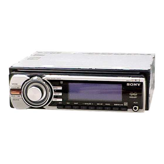
(Photo: CDX-GT710)
Model Name Using Similar Mechanism
CD Drive Mechanism Type
Optical Pick-up Name
SPECIFICATIONS
Selectivity
Signal-to-noise ratio
Harmonic distortion at 1 kHz
Separation
Frequency response
AM (CDX-GT71W/GT710: US, Canadian model/GT760)
Tuning range
AM tuning interval
Antenna terminal
Intermediate frequency 10.7 MHz/450 kHz
Sensitivity
FM/AM COMPACT DISC PLAYER
CDX-GT71W/GT710: US, Canadian Model/GT760
FM/MW/LW COMPACT DISC PLAYER
US Model
CDX-GT71W/GT710
Canadian Model
AEP Model
UK Model
CDX-GT710
E Model
Chinese Model
CDX-GT760
NEW
MG-101FA-188//Q
DAX-25A
75 dB at 400 kHz
67 dB (stereo), 69 dB (mono)
0.5% (stereo), 0.3% (mono)
35 dB at 1 kHz
30 – 15,000 Hz
CDX-GT71W/GT710: US, Canadian model:
530 – 1,710 kHz
CDX-GT760:
531 – 1,602 kHz (at 9 kHz step)
530 – 1,710 kHz (at 10 kHz step)
CDX-GT760:
9 kHz/10 kHz switchable
External antenna connector
30 µV
– Continued on next page –
CDX-GT710: AEP, UK Model
Advertisement
Table of Contents

Related Manuals for Sony CDX-GT71W


Summary of Contents for Sony CDX-GT71W
- Page 1 0.5% (stereo), 0.3% (mono) Separation 35 dB at 1 kHz Tuner section Frequency response 30 – 15,000 Hz AM (CDX-GT71W/GT710: US, Canadian model/GT760) Tuning range CDX-GT71W/GT710: US, Canadian model: 87.5 – 107.9 MHz Tuning range CDX-GT71W/GT710: US, Canadian model: CDX-GT710: AEP, UK model: 530 –...
- Page 2 REPLACE THESE COMPONENTS WITH SONY PARTS WHOSE NE REMPLACER CES COMPOSANTS QUE PAR DES PIÈCES PART NUMBERS APPEAR AS SHOWN IN THIS MANUAL OR SONY DONT LES NUMÉROS SONT DONNÉS DANS CE MANUEL IN SUPPLEMENTS PUBLISHED BY SONY. OU DANS LES SUPPLÉMENTS PUBLIÉS PAR SONY.
- Page 3 CDX-GT71W/GT710/GT760 • This compact disc player is classified as a CLASS 1 LASER UNLEADED SOLDER product. The CLASS 1 LASER PRODUCT label is located on the Boards requiring use of unleaded solder are printed with the lead- exterior. free mark (LF) indicating the solder contains no lead.
-
Page 4: Table Of Contents
CDX-GT71W/GT710/GT760 Ver. 1.2 TABLE OF CONTENTS SERVICE NOTE ............5 GENERAL Location of Controls ............6 Connections ..............8 DISASSEMBLY 3-1. Base Panel Assy ............... 17 3-2. Sub Panel Assy ..............17 3-3. CD Mechanism Block ............. 18 3-4. Driving Section (DB-F07) ..........18 3-5. -
Page 5: Service Note
CDX-GT71W/GT710/GT760 SECTION 1 SERVICE NOTE EXTENSION CABLE AND SERVICE POSITION When repairing or servicing this set, connect the jig (extension cable) as shown below. • Connect the MAIN board (CNP301) and the SERVO board (CN2) with the extension cable (Part No. J-2502-076-1). -
Page 6: General
CDX-GT71W/GT710/GT760 SECTION 2 GENERAL This section is extracted from instruction manual. • LOCATION OF CONTROLS • CDX-GT71W Location of controls and basic operations Main unit G RESET button (Location behind the front ql ENTER button panel) 4 To complete a setting. - Page 7 CDX-GT71W/GT710/GT760 • CDX-GT710: AEP, UK model Location of controls and basic operations Main unit G RESET button (Location behind the front ql ENTER button panel) 4 To complete a setting. w; </, (SEEK –/+) buttons H Disc slot 6 CD/MD* To insert the disc.
-
Page 8: Connections
CDX-GT71W/GT710/GT760 • CONNECTIONS • CDX-GT71W Connection example Notes (2- A ) • Be sure to connect the ground (earth) lead before connecting the amplifi er. AUDIO OUT • The alarm will only sound if the built-in amplifi er is used. - Page 9 CDX-GT71W/GT710/GT760 Source selector (not supplied) Supplied with the CD/MD changer Selector de fuente Suministrado con el cambiador de CD/MD (no suministrado) XA-C40 BUS AUDIO IN AUDIO OUT REMOTE FRONT SUB OUT (MONO) AUDIO AUDIO AUDIO REAR FRONT RCA pin cord (not supplied)
-
Page 10: Connection Example
CDX-GT71W/GT710/GT760 • CDX-GT710: US, Canadian model Connection example Notes (2- A ) • Be sure to connect the ground (earth) lead before connecting the amplifi er. AUDIO OUT • The alarm will only sound if the built-in amplifi er is used. - Page 11 CDX-GT71W/GT710/GT760 Source selector (not supplied) Supplied with the CD/MD changer Sélecteur de source Fourni avec le changeur de CD/MD (non fourni) XA-C40 BUS AUDIO IN AUDIO OUT REMOTE FRONT SUB OUT (MONO) AUDIO AUDIO AUDIO RCA pin cord (not supplied)
- Page 12 CDX-GT71W/GT710/GT760 • CDX-GT710: AEP, UK model Connection example Notes (2- A ) • Be sure to connect the ground (earth) lead before connecting the amplifi er. • The alarm will only sound if the built-in amplifi er is used. AUDIO OUT...
- Page 13 CDX-GT71W/GT710/GT760 Note for the aerial connecting Hinweis zum Anschließen der Antenne Remarque sur le raccordement de Nota per il collegamento dell’antenna Opmerking bij de antenne-aansluiting If your car antenna (aerial) is an Wenn Ihre Autoantenne der ISO-Norm ( l’antenne Se l’antenna dell’auto è di tipo...
- Page 14 CDX-GT71W/GT710/GT760 • CDX-GT760 Connection example Notes (2- A ) • Be sure to connect the ground (earth) lead before connecting the amplifi er. AUDIO OUT • The alarm will only sound if the built-in amplifi er is used. FRONT Tip (2- B - ) For connecting two or more CD/MD changers, the source selector XA-C40 (not supplied) is necessary.
- Page 15 CDX-GT71W/GT710/GT760 Source selector (not supplied) Selector de fuente Supplied with the CD/MD changer (no suminidtrado) Suministrado con el cambiador de CD/MD XA-C40 BUS AUDIO IN AUDIO OUT REMOTE FRONT SUB OUT (MONO) AUDIO AUDIO RCA pin cord (not supplied) AUDIO...
-
Page 16: Disassembly
CDX-GT71W/GT710/GT760 Ver. 1.2 SECTION 3 DISASSEMBLY Note: This set can be disassemble according to the following sequence. 3-1. BASE PANEL ASSY (Page 17) 3-2. SUB PANEL ASSY (Page 17) 3-3. CD MECHANISM BLOCK (Page 18) 3-4. DRIVING SECTION (DB-F07) 3-6. -
Page 17: Base Panel Assy
CDX-GT71W/GT710/GT760 Note: Follow the disassembly procedure in the numerical order given. 3-1. BASE PANEL ASSY 2 two screws (panel F) 5 bracket (PWB) 8 base panel assy 1 two screws (panel F) 6 FLEXIBLE board (36 core) (CN905) (Take care not to pull the... -
Page 18: Cd Mechanism Block
CDX-GT71W/GT710/GT760 3-3. CD MECHANISM BLOCK 7 CD mechanism block 5 two screws (+PTT 2.6 × 4) 6 bracket (CD) 2 screw (+PTT 2.6 × 6) 4 CNP301 1 screw (+PTT 2.6 × 6) 3-4. DRIVING SECTION (DB-F07) 3 screw (+PTT 2.6 × 6) -
Page 19: Main Board
CDX-GT71W/GT710/GT760 3-5. MAIN BOARD 9 two screws 8 screw (+P 2.6 × 8) 2 two screws 6 screw (+PTT 2.6 × 10) (+PTT 2.6 × 8) (+PTT 2.6 × 8) 0 two screws (+PTT 2.6 × 12) qd heat sink... -
Page 20: Chassis (T) Sub Assy
CDX-GT71W/GT710/GT760 3-7. CHASSIS (T) SUB ASSY 2 two precision screws 1 two precision screws (+P 1.7 × 2.2) (+P 1.7 × 2.2) 4 chassis (T) sub assy 3 claw 3-8. ROLLER ARM ASSY 5 roller arm assy 4 gear (RA1) -
Page 21: Chassis (Op) Assy
CDX-GT71W/GT710/GT760 Ver. 1.2 3-9. CHASSIS (OP) ASSY 6 chassis (OP) assy 1 tension spring (KF) 7 coil spring (damper) (natural) 8 coil spring (damper) (green) 4 slider (R) 3 lever (D) 2 gear (LE1) -
Page 22: Diagnosis Function
CDX-GT71W/GT710/GT760 SECTION 4 DIAGNOSIS FUNCTION Description of the Diagnostics function: 4. Contents of each display mode 4-1. Reset count display mode 1. Setting the Diag display mode DIAG With the power off, press the [4] button, [5] button, and [4] button on the set body or the remote control (for more than 2 seconds) in turn. - Page 23 CDX-GT71W/GT710/GT760 The display mode is switched by each rotation of [4/GP/ALBM+] or 4-4. Operating hours display mode [3/GP/ALBM--] keys during the CD error information display mode. DIAG XXXX CD error info history 1 (latest) Error description plus error details display...
- Page 24 CDX-GT71W/GT710/GT760 4-6. OFFSET/FAILURE error display mode DIAG XXXXX Operating hours Error description (0: OFFSET, 1: FAILURE) Recency of information 1-3: 1 represents the latest. Diag code 06: OFFSET/FAILURE The display mode is switched by each rotation of [4/GP/ALBM+] or [3/GP/ALBM--] keys during the OFFSET/FAILURE error display mode.
-
Page 25: Diagrams
CDX-GT71W/GT710/GT760 SECTION 5 DIAGRAMS 5-1. BLOCK DIAGRAM — MAIN SECTION — ELECTRONIC VOLUME PJ401 (1/2) IC401 PJ401 (2/2) AUDIO OUTR1 AUDIO OUT BUS-RCH OUTR2 R-CH REAR MUTE R-CH 1 BUS-LCH Q181 BUS-RCH 2 BUS-RCH OUTF1 CD L 5 CD-LCH AUDIO OUT... -
Page 26: Block Diagram -Display Section
CDX-GT71W/GT710/GT760 5-2. BLOCK DIAGRAM — DISPLAY SECTION — FL900 VACUUM DISPLAY CONTROL FLUORESCENT DISPLAYS IC901 85 KEY 1 KEY 2 MATRIX LAT TA2 OUT SYSTEM CONTROL VDD1 FL VDD+3.3V LSW901 (1/2)–915 (1/2) IC303 (2/2) S903,904, VDD2 FL VDD+55V 906 (2/2) - Page 27 CDX-GT71W/GT710/GT760 • NOTE FOR PRINTED WIRING BOARDS AND SCHEMATIC DIAGRAMS • WAVEFORMS — MAIN Board — — DISPLAY Board — THIS NOTE IS COMMON FOR PRINTED WIRING BOARDS AND SCHEMATIC DIAGRAMS. (In addition to this, the necessary note is IC303 8 (XCIN) IC901 qd (XIN) printed in each block.)
-
Page 28: Printed Wiring Boards -Main Section
CDX-GT71W/GT710/GT760 5-3. PRINTED WIRING BOARDS — MAIN SECTION — : Uses unleaded solder. • Semiconductor Location Ref. No. Location Ref. No. Location Ref. No. Location D101 B-10 D621 Q101 D-10 (D102) (D622) Q102 (D103) (D623) Q103 (D104) E-10 D625 Q110... - Page 29 CDX-GT71W/GT710/GT760 PJ401 CNJ101 CNP102 GT710:AEP,UK MODEL (REMOTE IN) (BUS CONTROL IN) R505 C232 C227 CNP102 C228 C188 C205 FB111 F901 C210 C215 C211 C242 C142 C288 C178 C278 IC201 D112 JR607 CNP101 R242 C112 R142 R185 R285 D110 D102 R175...
-
Page 30: Schematic Diagram -Main Section (1/4)
CDX-GT71W/GT710/GT760 • Refer to page 27 for Waveforms. 5-4. SCHEMATIC DIAGRAM — MAIN SECTION (1/4) — • Refer to page 37 for IC Block Diagrams. TUX501 Q501 L503 R486 R504 R501 C502 C501 D501 PJ501 IC B/D R505 R172 IC401... -
Page 31: Schematic Diagram -Main Section (2/4)
CDX-GT71W/GT710/GT760 5-5. SCHEMATIC DIAGRAM — MAIN SECTION (2/4) — • Refer to page 38 for IC Block Diagrams. PJ401 C215 C210 C228 C205 C227 CN401 FB402 IC B/D C278 C178 C142 C242 D111 C442 C188 C288 D110 C443 R402 R142... -
Page 32: Schematic Diagram -Main Section (3/4)
CDX-GT71W/GT710/GT760 • Refer to page 27 for Waveforms. • Refer to page 39 for IC Block Diagrams. 5-6. SCHEMATIC DIAGRAM — MAIN SECTION (3/4) — • Refer to page 41 for IC Pin Description of IC303. (Page 30) (Page 31) -
Page 33: Schematic Diagram -Main Section (4/4)
CDX-GT71W/GT710/GT760 5-7. SCHEMATIC DIAGRAM — MAIN SECTION (4/4) — • Refer to page 40 for IC Block Diagrams. (Page 31) CN801 Q301 L304 Q642 R625 R318 C632 R319 Q302 Q623 L502 C622 L620 Q624 C512 (Page 30) C340 C342 D814... -
Page 34: Printed Wiring Boards -Display Section
CDX-GT71W/GT710/GT760 5-8. PRINTED WIRING BOARDS — DISPLAY SECTION — : Uses unleaded solder. LSW915 S904 LSW915 LSW901 LED926 LSW906 LSW905 LSW902 LED923 LSW904 LSW903 LSW912 LSW911 LSW910 LSW909 LSW908 LSW907 LSW913 LSW914 S903 • Semiconductor Location Ref. No. Location Ref. No. -
Page 35: Printed Wiring Board -Base Panel Section
CDX-GT71W/GT710/GT760 5-9. PRINTED WIRING BOARD — BASE PANEL SECTION — : Uses unleaded solder. S902 S901 CN904 (NOSE DET) RESET (Page 28) MAIN BOARD CN801 DISPLAY BOARD CN902 (Page 34) CDX-GT71W/GT710/GT760... -
Page 36: Schematic Diagram -Display Section
CDX-GT71W/GT710/GT760 • Refer to page 27 for Waveforms. 5-10. SCHEMATIC DIAGRAM — DISPLAY SECTION — • Refer to page 44 for IC Pin Description of IC901. R982 LSW915(1/2) R981 IC903 EXCEPT GT710:AEP,UK R920 R921 R922 R923 R924 R925 R926 R927... -
Page 37: Ic Block Diagrams
CDX-GT71W/GT710/GT760 • IC BLOCK DIAGRAMS IC401 BD3442FS-E2 (MAIN Board (1/4)) BUS-L 32 FIL VCC2 100k 31 GND BUS-R INPUT INPUT VOLUME1 TREBLE VOLUME2 100k SELECTOR GAIN /MUTE /BASS TU-L 3 30 SDA /MIDDLE 100k LOGIC 29 SCL TU-R 28 MUTE... - Page 38 CDX-GT71W/GT710/GT760 IC201 TDA8588AJ/N2/R1 (MAIN Board (2/4)) OUT-FL– C BUS OUT-FL+ OUT-RL– PGND3 OUT-RL+ IN-RL IN-FL S-GND PROTECTION/ DIAGNOSTIC IN-FR IN-RR AC_GND OUT-RR+ PGND2 OUT-RR– OUT-FR+ STANDBY/ MUTE OUT-FR– CHIP DETECT/ PGND1 DIAGNOSTIC BATTERY TEMPERATURE DIAG DETECTION PROTECTION ENABLE LOGIC SW2(ANT-REM)
- Page 39 CDX-GT71W/GT710/GT760 IC702 LB1930M-TLM-E (MAIN Board (3/4)) BUFFER OUT1 MOTOR CONTROL DRIVE CIRCUIT CIRCUIT OUT2 BUFFER SGND PGND IC703 BA09CCOWFP-E2 (MAIN Board (3/4)) VREF DRIVER...
- Page 40 CDX-GT71W/GT710/GT760 IC620 NJM2377M (TE2) (MAIN Board (4/4)) 30µA VREF U.VLO S.C.P ER.AMP 0.52V IC110 BA8271F-E2 (MAIN Board (4/4)) BUS ON BUS ON SWITCH RESET RESET SWITCH BUS ON CLK IN BATTERY BATT BU IN SWITCH VREF DATA IN DATA DATA OUT...
- Page 41 DST SEL0 Destination setting pin 0 FSW IN D/D converter oscillator frequency count control signal input UNI SO SONY bus serial data signal output UNI SI SONY bus serial data signal input UNI CKO SONY bus serial clock signal output BYTE Connect to ground.
- Page 42 CDX-GT71W/GT710/GT760 Pin No. Pin Name Pin Description OPEN REQ CD mechanism open request signal input EJECT OK CD mechanism eject control signal output P MONITOR P-SNSR process monitor signal output CD ON CD servo power supply on/off control signal input...
- Page 43 CDX-GT71W/GT710/GT760 Pin No. Pin Name Pin Description VREF — Reference voltage pin for A/D converter AVCC — Power supply pin (+3.3 V) DISP SI/RX Communication signal input from display IC DISP SO/TX Communication signal output to display IC DISP CKO...
- Page 44 CDX-GT71W/GT710/GT760 IC901 M30876FJBA01GP (DISPLAY CONTROL) (DISPLAY BOARD) Pin No. Pin Name Pin Description SYS CE Main chip enable signal input Not used in this set. (Open) FL DAT3 Vacuum fluorescent displays serial data signal output 3 Not used in this set. (Open)
- Page 45 CDX-GT71W/GT710/GT760 Pin No. Pin Name Pin Description ILL RED Illumination (red) change control signal output Dimmer control signal output AVSS — Ground pin Not used in this set. (Open) VREF — Reference voltage power supply pin (+3.3 V) AVCC —...
-
Page 46: Exploded Views
CDX-GT71W/GT710/GT760 Ver. 1.2 SECTION 6 EXPLODED VIEWS NOTE: • The mechanical parts with no reference • -XX and -X mean standardized parts, so The components identified by mark 0 or dotted line with mark number in the exploded views are not supplied. -
Page 47: Main Board Section
CDX-GT71W/GT710/GT760 Ver. 1.2 6-2. MAIN BOARD SECTION not supplied TUX501 not supplied not supplied Ref. No. Part No. Description Remark Ref. No. Part No. Description Remark A-1224-588-A MAIN BOARD, COMPLETE (US,CND) TUX501 A-3220-961-B TUNER UNIT (TUX-032) A-1225-591-A MAIN BOARD, COMPLETE (AEP,UK) 7-685-792-09 SCREW +PTT 2.6X6 (S) -
Page 48: Front Panel Section
CDX-GT71W/GT710/GT760 Ver. 1.1 6-3. FRONT PANEL SECTION not supplied (DISPLAY board) not supplied FL900 not supplied not supplied not supplied not supplied not supplied not supplied not supplied not supplied (AUX board) Ref. No. Part No. Description Remark Ref. No. -
Page 49: Cd Mechanism Section (Mg-101Fa-188//Q)
CDX-GT71W/GT710/GT760 Ver. 1.2 6-4. CD MECHANISM SECTION (MG-101FA-188//Q) NOTE: Refer to SUPPLEMENT-1 for disassembly of OPTICAL PICK-UP. not supplied not supplied not supplied not supplied not supplied not supplied not supplied not supplied not supplied not supplied not supplied Ref. No. -
Page 50: Electrical Parts List
CDX-GT71W/GT710/GT760 Ver. 1.2 SECTION 7 BASE PANEL DISPLAY ELECTRICAL PARTS LIST NOTE: • Due to standardization, replacements in • Items marked “*” are not stocked since The components identified by mark 0 or dotted line with mark the parts list may be different from the they are seldom required for routine service. - Page 51 CDX-GT71W/GT710/GT760 DISPLAY Ref. No. Part No. Description Remark Ref. No. Part No. Description Remark < JUMPER RESISTOR > R911 1-216-820-11 METAL CHIP 1/10W R912 1-216-821-11 METAL CHIP 1/10W JC902 1-216-864-11 SHORT CHIP R913 1-216-822-11 METAL CHIP 1.2K 1/10W JC907 1-216-864-11 SHORT CHIP...
- Page 52 CDX-GT71W/GT710/GT760 Ver. 1.2 DISPLAY MAIN Ref. No. Part No. Description Remark Ref. No. Part No. Description Remark < VIBRATOR > C229 1-115-340-11 CERAMIC CHIP 0.22uF C232 1-107-826-11 CERAMIC CHIP 0.1uF X901 1-813-522-21 VIBRATOR, CERAMIC (6.75MHz) C236 1-165-908-11 CERAMIC CHIP C237...
- Page 53 CDX-GT71W/GT710/GT760 MAIN Ref. No. Part No. Description Remark Ref. No. Part No. Description Remark C425 1-124-717-85 ELECT C628 1-164-004-11 CERAMIC CHIP 0.1uF (AEP,UK) C629 1-126-933-11 ELECT 100uF C425 1-126-960-11 ELECT C630 1-164-004-11 CERAMIC CHIP 0.1uF (EXCEPT AEP,UK) C632 1-107-826-11 CERAMIC CHIP 0.1uF...
- Page 54 CDX-GT71W/GT710/GT760 MAIN Ref. No. Part No. Description Remark Ref. No. Part No. Description Remark D402 6-500-335-01 DIODE MC2838-T112-1 JR618 1-216-295-11 SHORT CHIP D404 8-719-057-80 DIODE MA8180-M-TX D501 8-719-977-03 DIODE DTZ5.6B < COIL > D620 8-719-053-18 DIODE 1SR154-400TE-25 D621 8-719-053-18 DIODE 1SR154-400TE-25...
- Page 55 CDX-GT71W/GT710/GT760 Ver. 1.2 MAIN Ref. No. Part No. Description Remark Ref. No. Part No. Description Remark R106 1-216-841-11 METAL CHIP 1/10W R314 1-216-843-11 METAL CHIP 1/10W R107 1-216-073-00 RES-CHIP 1/10W R315 1-216-842-11 METAL CHIP 1/10W R108 1-216-073-00 RES-CHIP 1/10W R318...
- Page 56 CDX-GT71W/GT710/GT760 Ver. 1.2 MAIN SERVO SUB PANEL Ref. No. Part No. Description Remark Ref. No. Part No. Description Remark R392 1-216-845-11 METAL CHIP 100K 1/10W R640 1-216-845-11 METAL CHIP 100K 1/10W R400 1-216-864-11 SHORT CHIP R644 1-216-134-00 RES-CHIP 1/8W R401...
- Page 57 CDX-GT71W/GT710/GT760 Ver. 1.2 Ref. No. Part No. Description Remark Ref. No. Part No. Description Remark MISCELLANEOUS PARTS FOR INSTALLATION AND CONNECTIONS *************** *************************************** 1-831-837-11 CORD (WITH CONNECTOR) (ISO) (POWER) X-3382-647-1 FRAME ASSY, FITTING (AEP,UK) 2-698-362-01 COLLAR 1-833-102-11 CORD (WITH CONNECTOR) (POWER)
- Page 58 CDX-GT71W/GT710/GT760 MEMO...
- Page 59 CDX-GT71W/GT710/GT760 US Model CDX-GT71W/GT710 Canadian Model SERVICE MANUAL AEP Model UK Model Ver. 1.2 2007.03 CDX-GT710 E Model Chinese Model CDX-GT760 SUPPLEMENT-1 File this supplement with the service manual. Subject: Notes for removal of the OPTICAL PICK-UP added. DISASSEMBLY 1. CHUCKING ARM SUB ASSY...
- Page 60 CDX-GT71W/GT710/GT760 2. SLED MOTOR ASSY 2 three serration screws (M 2 × 3) 3 sled mtor assy 1 spring turn table spring stand Note: Never remove these parts since they were adjusted. stand Note: Place the stand with care not to touch the turn table.
- Page 61 CDX-GT71W/GT710/GT760 3. OPTICAL PICK-UP SECTION 2 optical pick-up section Note: Be careful not to touch the lens and hologram terminal when removing the optical pick-up section. 4. OPTICAL PICK-UP 1 pan tapping screw (M 1.4 × 2.5) 2 leaf spring (sub guide)
- Page 62 CDX-GT71W/GT710/GT760 REVISION HISTORY Clicking the version allows you to jump to the revised page. Also, clicking the version at the upper on the revised page allows you to jump to the next revised page. Ver. Date Description of Revision 2006.12 2007.01...
Need help?
Do you have a question about the CDX-GT71W and is the answer not in the manual?
Questions and answers