
Subscribe to Our Youtube Channel
Related Manuals for MiTAC 9223


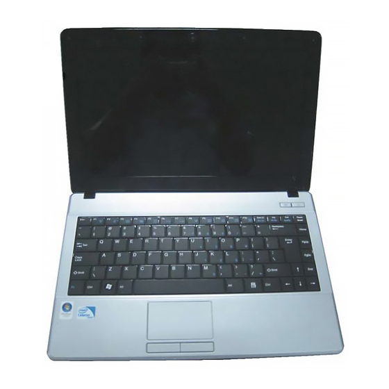
Summary of Contents for MiTAC 9223
- Page 1 SERVICE MANUAL FOR SERVICE MANUAL FOR 9223 9223 BY: Meg.chen Technical Maintenance Department/GTK MTC Nov.2009/R00...
-
Page 2: Table Of Contents
9223 N/B Maintenance 9223 N/B Maintenance Contents 1. Hardware Engineering Specification ……………………………………………………………………. 1.1 Introduction ……………………………………………………………………………………………………………… 1.2 System Overview ………………………………………………………………………………………...……………… 1.3 Functions Description …………………………………………………………………………………………….……. 1.4 Electrical Characteristic ………………………………………………………………………………..……………… 1.5 Reference Documents …………………………………………………………………………………………………… 2. System View and Disassembly …………………………………………………………………………..2.1 System View ………………………………………………………………………………………………………………... - Page 3 9223 N/B Maintenance 9223 N/B Maintenance Contents 5. System Block Diagram …………………………………………………………………………………….. 6. Trouble Shooting ………………………………………………………………………………………………………….. 6.1 No Power………………………………………………………………………………………………………………….. 6.2 No Display………………………………………………………………………………………………………………… 6.3 Graphics Controller Failure LCD No Display………………………………………………………………………… 6.4 External Monitor No Display…………………………………………………………………………………………… 6.5 Keyboard (K/B) & Touch-Pad (T/P) Failure……………………………………………………………………………...
-
Page 4: Hardware Engineering Specification
1.1 Introduction 1.1.1 General Description The 9223 motherboard is Intel Montevina SFF Platform with Mobile Penryn ULV on Intel’s advance 45 nm process technology with copper interconnect. The processor provides a high-performance low-power mobile processor based on the Intel Mobile processor architecture. -
Page 5: System Overview
9223 N/B Maintenance 9223 N/B Maintenance 1.2 System Overview Basic Function Spec Remark CPU 10W Type Mobile Penryn Montevina ULV CPU SU2700 Montevina SFF SKU Mobile Penryn Montevina Celeron CPU C723 FSB 800 10W TDP chassis design Chipset NB low 7-8W,high 10-12.5W, SB 2.0-2.5W... - Page 6 9223 N/B Maintenance 9223 N/B Maintenance Continue to the previous page Graphic Audio Interface Azalia ALC 272 Speaker 1.5W speaker x2 with Speaker Box Int. Mic 1 mic array Volume S/W volume control by K/B Quality Buzzer Not Support Express Card...
- Page 7 9223 N/B Maintenance 9223 N/B Maintenance Continue to the previous page Communication Spec Remark Conn. I/F RJ45 Jack RTL8111DL Slot Type On board LAN solution Spec 10/100/1000 LAN (PCI-E) Function Boot on LAN Wake on LAN in S3 Wake on LAN in S4...
- Page 8 9223 N/B Maintenance 9223 N/B Maintenance Continue to the previous page Wireless LAN Slot Type Mini PCI-E x2 Antenna MIMO 1.3G (EU first) + MIMO + BT for antenna (US 2 priority) 2.All Antenna on top Module Spec 1.802.11 b/g/n , AW-NE771 MIMO 2.3G , EM770...
- Page 9 9223 N/B Maintenance 9223 N/B Maintenance Continue to the previous page Bluetooth BTO if possible Slot Type 8 pin Test criteria: 1Mbps @10m Antenna Antenna on panel top Module Spec AW-BT252 Others Power on status Webcam Slot Type Module Spec...
- Page 10 9223 N/B Maintenance 9223 N/B Maintenance Continue to the previous page Storage Device Spec Remark SATA I/F,2.5’’ height HDD 160/250/320 GB 9.5mm height ODD SATA interface Type Super Multi/DVD-Dual/DVD COMBO Digital support only Structure I/O Interface Spec Remark Video output...
- Page 11 9223 N/B Maintenance 9223 N/B Maintenance Continue to the previous page Status LED WLAN Blue AC/BATT Blue/Red Charge Blue HDD/ODD Blue Caps Lock Blue Num Lock Blue PWR button Blue ECO button Blue Input Device Spec Remark Keyboard 19mm Pitch/1.7mm Stroke...
- Page 12 9223 N/B Maintenance 9223 N/B Maintenance Continue to the previous page 300mm Dimension Beep Function Key Fn+F1 (WLAN) Windows Radio on/off Radio on/off Fn+F3 Windows Sound down Fn+F4 Windows Sound up Fn+F5 Dos/Windows Behaviour: Display Change LCD→LCD+CRT→CRT→LCD Brightness down Fn+F6 16 levels...
- Page 13 9223 N/B Maintenance 9223 N/B Maintenance Continue to the previous page Pointing Device Synaptics: TM391 Under plastic Function Glide pad with 2 buttons 12 Pin Power Spec Remark Battery Gauge IC 20Z90 Type Li-ion type Capacity 2250mAh Cells No. 6 cells...
- Page 14 9223 N/B Maintenance 9223 N/B Maintenance Continue to the previous page AC Adapter 65W 3 pin DC Input AC 100-240V Vendor Delta Leakage Current Battery remain 20% after 30 Days w/z 100% battery capacity (6 cell)
-
Page 15: Functions Description
9223 N/B Maintenance 9223 N/B Maintenance 1.3 Function Description 1.3.1 CPU • The Penryn Processor SU2700 on 45-nanometer process technology (also referred to as CPU and processor in this document) with the following new features: • 800-MTs Source-Synchronous Front Side Bus (FSB) •... - Page 16 9223 N/B Maintenance 9223 N/B Maintenance Cantiga • The Cantiga chipset Graphics Memory Controller Hub (also referred to as the (G)MCH in the document) and ICH9M I/O controller hub with the following new features. • Gen 5.0 Integrated Graphics Engine •...
- Page 17 9223 N/B Maintenance 9223 N/B Maintenance 1.3.3 Memory Support DDR2 667/800 MHz SO-DIMM expandable to 4GB (2 DDR2-SODIMM slots) Slot1 Slot2 Total 1.3.4 I/O PORTS CRT Port • Standard VGA compatible port • DDC1 and DDC2B compliant...
- Page 18 9223 N/B Maintenance 9223 N/B Maintenance SIGNAL DESCRIPTION CRT_RED Red analog video output CRT_GREEN Green analog video output CRT_BLUE Blue analog video output Monitor Sense Monitor Sense Ground Ground Ground +5VDC Ground Monitor Sense CRT_DDDA Data from DDC monitor CRT_HSYNC...
- Page 19 9223 N/B Maintenance 9223 N/B Maintenance • The Fast Ethernet MAC Controller features an IEEE802.3 and IEEE802.3x compliant MAC with external LAN physical layer chip supporting full duplex control. • Support Wake-up On-LAN function from S3. Signal Name Direction Description...
- Page 20 9223 N/B Maintenance 9223 N/B Maintenance • Support maximum transfer rate up to 480Mbits/s Signal Name Direction Description Power USB Device Power (+5VDC) DATA- Balanced Data Negative DATA+ Balanced Data Positive Ground Ground Card Reader Port • Support SD, MMC, Memory Stick, Memory Stick Duo (adapter), Memory Stick Pro.
-
Page 21: Power Management Features
9223 N/B Maintenance 9223 N/B Maintenance 1.3.5 DISPLAY 13.3” WXGA(1366x768 pixels) display size for notebook PC LED Backlight with LED controller IC Glare Surface Bezel less structure 1.3.6 READ ONLY MEMORY (SPI Serial Flash) Fully compatible with industry standard software including Windows Vista. -
Page 22: Keyboard Controller
9223 N/B Maintenance 9223 N/B Maintenance CPU Idle mode (Including ACPI modes C0, C1, C2, C3,C4 and C6) Suspend mode (S3 & S4 ACPI modes) Fully APM-base legacy power. Fully ACPI V1.0b, 2.0 and 3.0, compliant. Hibernate for Vista. Thermal management. -
Page 23: Electrical Characteristic
9223 N/B Maintenance 9223 N/B Maintenance 1.4 Electrical Characteristic 1.4.1 Power Consumption Of Suspend Mode Suspend To RAM < 50mA Suspend To Disk / Soft-Off /Mechanical Off < 1mA Power Spec Remark Battery Gauge IC 20Z90 Type Li-ion type Capacity 2250mAh (P) (S) Cells No. - Page 24 9223 N/B Maintenance 9223 N/B Maintenance Power off Charge Target:2 hrs to 90%(6 cells ) Power on Charge Target: TBD Idle mode S3 Suspend Time Target: TBD RTC Battery Not chargeable 5 years battery life AC Adapter 65W 3 pin DC...
-
Page 25: Reference Documents
9223 N/B Maintenance 9223 N/B Maintenance 1.5 Reference Documents Documents Revision Montevina Platform Design Guide for Penryn Processor, Cantiga Chipset and ICH9M I/O Controller Hub Penryn Processor for Montevina Platform Cantiga Chipset External Design Specification (EDS) Intel® I/O Controller Hub 9 (ICH9) Family External Design Specification (EDS) – Volume 1 Realtek ALC272 Realtek RTS5159 USB 2.0 Card Reader Controller... - Page 26 9223 N/B Maintenance 9223 N/B Maintenance Appendix B Function Key Definition Function Key Radio on/off Fn+F1 (WLAN) w/o bibi sound Radio on/off Fn+F1 (Bluetooth) Sound down Fn+F3 w/o bibi sound Sound up Fn+F4 w/o bibi sound Display Change Fn+F5 W/o bibi sound...
-
Page 27: System View And Disassembly
9223 N/B Maintenance 9223 N/B Maintenance 2. System View and Disassembly 2.1 System View 2.1.2 Left-side View Power Connector VGA Port USB Port RJ-45 Connector Card Reader Express card slot 2.1.2 Right-side View Super Multi Drive Audio output Connector Microphone Connector... - Page 28 9223 N/B Maintenance 9223 N/B Maintenance 2.1.3 Bottom View Battery Pack Stereo Speaker 2.1.4 Top-open View Camera LCD Screen Microphone Power Button ECO Button Keyboard Touch Pad Indicators...
-
Page 29: Tools Introduction
9223 N/B Maintenance 9223 N/B Maintenance 2.2 Tools Introduction 1. Screw driver with bit size for notebook assembly & disassembly. 2 mm 2 mm 2. Auto screw driver for notebook assembly & disassembly. Bit Size Screw Size Tooling Tor. Bit Size 1. -
Page 30: System Disassembly
9223 N/B Maintenance 9223 N/B Maintenance 2.3 System Disassembly The section discusses at length each major component for disassembly/reassembly and show corresponding illustrations.Use the chart below to determine the disassembly sequence for removing components from the notebook. NOTE: Before you start to install/replace these modules, disconnect all peripheral devices and make sure the notebook is not turned on or connected to AC power. -
Page 31: Battery Pack
9223 N/B Maintenance 9223 N/B Maintenance 2.3.1 Battery Pack Disassembly 1. Carefully put the notebook upside down. 2. Slide two release levers outwards to the “unlock” ( ) position ( ), while take the battery pack out of the compartment ( ). (Figure 2-1) - Page 32 9223 N/B Maintenance 9223 N/B Maintenance 2.3.2 ODD Disassembly 1. Remove the battery pack. (Refer to section 2.3.1 Disassembly) 2. Remove one screw fastening the CD-ROM module to free the ODD (Figure 2-2) Figure 2-2 Remove the ODD Reassembly 1. Replace the ODD module, then secure with one screw.
- Page 33 9223 N/B Maintenance 9223 N/B Maintenance 2.3.3 KBD Disassembly 1. Remove the battery pack. (See section 2.3.1 Disassembly) 2. Loosen the six latches locking the keyboard. (Figure 2-3) 3. Slightly lift up the keyboard and disconnect the cable from the mother board, then separate the keyboard (Figure 2-4)
- Page 34 9223 N/B Maintenance 9223 N/B Maintenance 2.3.4 Housing Disassembly 1. Remove the battery pack, ODD. (See section 2.3.1~2.3.2 Disassembly) 2. Remove sixteen screws and two Dummy card to free the housing. ( Figure 2-5~2-6) Figure 2-6 Remove the two dummy card...
- Page 35 9223 N/B Maintenance 9223 N/B Maintenance 2.3.5 DDR Disassembly 1. Remove the battery pack, ODD, Housing. (See section 2.3.1~2.3.2, 2.3.4 Disassembly) 2. Pull the retaining clips outwards ( ) and remove the SO-DIMM ( ). (Figure 2-7) Figure 2-7 Remove the SO-DIMM Reassembly 1.
- Page 36 9223 N/B Maintenance 9223 N/B Maintenance 2.3.6 Wlan Disassembly 1. Remove the battery pack, ODD, Housing. (Refer to section 2.3.1~2.3.2, 2.3.4 Disassembly) 2. Disconnect the two antennae first, then remove two screws to free the wlan. (Figure 2-8) Figure 2-8 Free the Wlan Reassembly 1.
- Page 37 9223 N/B Maintenance 9223 N/B Maintenance 2.3.7 HDD Disassembly 1. Remove the battery pack, ODD, Housing, WLAN. (Refer to section 2.3.1~2.3.2, 2.3.4~2.3.6 Disassembly) 2. Remove the one screw and slide the HDD module out of the compartment. (Figure 2-9) Figure 2-9 Remove HDD Reassembly 1.
- Page 38 9223 N/B Maintenance 9223 N/B Maintenance 2.3.8 Heatsink Disassembly 1. Remove the battery pack, ODD, Housing, WLAN, HDD. (Refer to section 2.3.1~2.3.2, 2.3.4~2.3.7 Disassembly) 2. Remove five screws that secure with heatsink and disconnect the cable from system board. (Figure 2-10)
- Page 39 9223 N/B Maintenance 9223 N/B Maintenance 2.3.9 Audio BD Disassembly 1. Remove the battery pack, ODD, Housing, WLAN, HDD, Heatsink. (Refer to section 2.3.1~2.3.2, 2.3.4~2.3.8 Disassembly) 2. Disconnect the three cables from audio board then remove one screw that secure with audio Board. (Figure 2-11)
- Page 40 9223 N/B Maintenance 9223 N/B Maintenance 2.3.10 HDD ODD Board Disassembly 1. Remove the battery pack, ODD, Housing, WLAN, HDD, Heatsink, Audio board. (Refer to section 2.3.1~2.3.2, 2.3.4~2.3.9 Disassembly) 2. Disconnect the cable from system board then pick up the HDD ODD board. (Figure 2-12)
-
Page 41: System Board
9223 N/B Maintenance 9223 N/B Maintenance 2.3.11 System Board Disassembly 1. Remove the battery pack, ODD, Housing, WLAN, HDD, Heatsink, Audio board, HDD ODD board. (Refer to section 2.3.1~2.3.2, 2.3.4~2.3.10 Disassembly) 2. Disconnect the three cables and remove threes screws from system board. (Figure 2-13) 3. - Page 42 9223 N/B Maintenance 9223 N/B Maintenance 2.3.12 Bluetooth Disassembly 1. Remove the battery pack, ODD, Housing, WLAN, HDD, Heatsink, Audio board, HDD ODD board, System board. (Refer to section 2.3.1~2.3.2, 2.3.4~2.3.11 Disassembly) 2. Remove one screw to free the Bluetooth board. (Figure 2-15)
- Page 43 9223 N/B Maintenance 9223 N/B Maintenance 2.3.13 Speaker Disassembly 1. Remove the battery pack, ODD, Housing, WLAN, HDD, Heatsink, Audio board, HDD ODD board, System board, Bluetooth. (Refer to section 2.3.1~2.3.2, 2.3.4~2.3.12 Disassembly) 2. Remove four screws to free the speaker. (Figure 2-16)
-
Page 44: Lcd Assy
9223 N/B Maintenance 9223 N/B Maintenance 2.3.14 LCD ASSY Disassembly Housing, WLAN, HDD, Heatsink, Audio board, HDD ODD board, Remove the battery pack, ODD, System board, Bluetooth, Speaker. (Refer to section 2.3.1~2.3.2, 2.3.4~2.3.13 Disassembly) 2. Remove two screws to free the LCD ASSY. (Figure 2-17) -
Page 45: Lcd Panel
9223 N/B Maintenance 9223 N/B Maintenance 2.3.15 LCD Panel Disassembly 1. Remove the battery pack, ODD, Housing, WLAN, HDD, Heatsink, Audio board, HDD ODD board, System board, Bluetooth, Speaker, lcd assy. (Refer to section 2.3.1~2.3.2, 2.3.4~2.3.14 Disassembly) 2. Remove two screws fastening the LCD cover. (Figure 2-18) 3. -
Page 46: Definition & Location Of Connectors/Switches
9223 N/B Maintenance 9223 N/B Maintenance 6. Remove four screws fastening the LCD panel. (Figure 2-20) 7. Disconnect the cable to free the LCD panel. (Figure 2-21) Figure 2-20 Remove four screws Figure 2-21 Remove cable Reassembly 1. Replace the cable to the LCD, then replace LCD panel into the LCD housing and secure with four screws 2. -
Page 47: Mother Board
9223 N/B Maintenance 9223 N/B Maintenance Major Components 3. Definition & Location of 3.1 Mother Board (Side A) PJ501 : Power Connector J501 : VGA Connector J501 J502 J503 PJ501 J502 : USB Connector J508 J504 J503 : RJ45 Connector... - Page 48 9223 N/B Maintenance 9223 N/B Maintenance Major Components 3. Definition & Location of 3.1 Mother Board (Side B) J1 : Express Card Socket U5 : ICH9M South Bridge U9 : Keyboard Controller J4 : MB to Audio board J2 : Keyboard Connector...
-
Page 49: Pin Descriptions Of Major Components
9223 N/B Maintenance 9223 N/B Maintenance 4. Pin Descriptions of Major Components Cantiga North Bridge -1 Host Interface Signals Signal Name Type Description H_A#[35:3] Host Address Bus: HA#[35:3] connects to the processor AGTL+ 2X address bus. During processor cycles the HA#[35:3] are inputs. - Page 50 9223 N/B Maintenance 9223 N/B Maintenance Cantiga North Bridge -2 H_BREQ# Host Bus Request: The (G)MCH pulls the processor bus AGTL+ H_BREQ# signal low during H_CPURST#. The signal is ampled by the processor on the active-to-inactive transition of H_CPURST#. H_BREQ# should be tri-stated after the hold tim requirement has been satisfied.
- Page 51 9223 N/B Maintenance 9223 N/B Maintenance Cantiga North Bridge -3 H_DINV#[3:0] Host Dynamic Bus Inversion: Driven along with the AGTL+ HD[63:0]# signals. Indicates if the associated signals are inverted or not. HDINV[3:0]# are asserted such that the number of data bits driven electrically low (low voltage) within the corresponding 16-bit group never exceeds 8.
- Page 52 9223 N/B Maintenance 9223 N/B Maintenance Cantiga North Bridge -4 Host Interface Signals(continued) Signal Name Type Description H_HIT# Host Hit: Indicates that a caching agent holds an unmodified AGTL+ version of the requested line. Also, driven in conjunction with H_HITM# by the target to extend the snoop window.
- Page 53 9223 N/B Maintenance 9223 N/B Maintenance Cantiga North Bridge -5 Host Interface Signals(continued) Signal Name Type Description THERMTRIP# Connects between the Processor, (G)MCH and the ICH. AGTL+ Assertion of THERMTRIP# (Thermal Trip) indicates the (G)MCH junction temperature has reached a level beyond which damage may occur.
- Page 54 9223 N/B Maintenance 9223 N/B Maintenance Cantiga North Bridge -6 SA_DQS#[7:0] Data Strobe Complements: These are the SSTL-1.8/1.5 complementary strobe signals. SA_DQ[63:0] Data Bus: Channel A data signal interface to the SDRAM data bus SSTL-1.8/1.5 SA_MA[14:0] Memory Address: These signals are used to provide the SSTL-1.8/1.5 multiplexed row and column address to the SDRAM.
- Page 55 9223 N/B Maintenance 9223 N/B Maintenance Cantiga North Bridge -7 Memory Channel B Interface Signal Name Type Description SB_BS[2:0] Bank Select: These signals define which banks are SSTL-1.8/1.5 selected within each SDRAM rank. SB_WE# Write Enable Control Signal: Used with SB_RAS# and SSTL-1.8/1.5 SB_CAS# (along with SB_CS#) to define the SDRAM...
- Page 56 9223 N/B Maintenance 9223 N/B Maintenance Cantiga North Bridge -8 Memory Channel B Interface(continued) Signal Name Type Description SB_DQ[63:0] Data Bus: Channel B data signal interface to the SDRAM SSTL-1.8/1.5 data bus. SB_CK[1:0] SDRAM Differential Clock: Channel B SDRAM SSTL-1.8/1.5 Differential Clock signal-pair. The crossing of the positive...
- Page 57 9223 N/B Maintenance 9223 N/B Maintenance Cantiga North Bridge -9 PCI Express Based Graphics Interface Signals Signal Name Type Description PEG_COMPI PEG_COMPI PCI Express Graphics Input Current Compensation PEG_COMPO PCI Express Graphics Output Current and Resistance Compensation PEG_RX[15:0] PCI Express Graphics Receive Differential Pair...
- Page 58 9223 N/B Maintenance 9223 N/B Maintenance Cantiga North Bridge -10 CRT DAC Signals(continued) Signal Name Type Description CRT_VSYNC CRT Vertical Synchronization: This signal is used as the HVCMOS vertical sync (polarity is programmable). CRT_HSYNC CRT Horizontal Synchronization: This signal is used as the HVCMOS horizontal sync (polarity is programmable) or “sync interval”.
- Page 59 9223 N/B Maintenance 9223 N/B Maintenance Cantiga North Bridge -11 LVDS Signals Signal Name Type Description LDVS Channel A LVDSA_CLK LVDS Channel A differential clock output – positive LVDS LVDSA_CLK# LVDS Channel A differential clock output – negative LVDS LVDSA_DATA# LVDS Channel A differential data output –...
- Page 60 9223 N/B Maintenance 9223 N/B Maintenance Cantiga North Bridge -12 LVDS Reference Signals LVDS_IBG LVDS Reference Current LVDS_VBG Leave as NC LVDS_VREFH Must be connected to ground. LVDS_VREFL Must be connected to ground. Display Data Channel (DDC) and GMBUS Support...
- Page 61 9223 N/B Maintenance 9223 N/B Maintenance Cantiga North Bridge -13 IntelR High Definition Audio (IntelR HD Audio) Signals Signals Type Description HDA_SDO Intel HD Audio Serial Data Input to (G)MCH Audio CMOS HW: Driven by Intel HD Audio Controller. HDA_SDI...
- Page 62 9223 N/B Maintenance 9223 N/B Maintenance Cantiga North Bridge -14 PLL Signals Signal Name Type Description DPLL_REF_CLK Display PLLA Differential Clock In: 96 MHz Diff Clk Display PLL Differential Clock In, no SSC support – DPLL_REF_CLK Display PLLA Differential Clock In Complement:...
- Page 63 9223 N/B Maintenance 9223 N/B Maintenance Cantiga North Bridge -15 Reset and Miscellaneous Signals Signal Name Type Description CLKREQ# External Clock Request: (G)MCH drives CLKREQ# to control the PCI Express differential clock input to itself. GFX_VID[4:0] Voltage ID to support Graphics Render Standby...
- Page 64 9223 N/B Maintenance 9223 N/B Maintenance Cantiga North Bridge -16 Reset and Miscellaneous Signals(continued) Signal Name Type Description TSATN# Thermal Sensor Aux Trip Notification: Output from the AGTL+ (G)MCH to the EC indicating the Aux2 trip point (SW programmable) has been crossed.
- Page 65 9223 N/B Maintenance 9223 N/B Maintenance Cantiga North Bridge -17 Power and Ground (Sheet 2 of 3) Voltage Ball Name Description 1.05 VCCA_SM_CK Clock logic voltage PCI Express* Based Graphics / DMI 1.05 VCC_PEG Analog, I/O Logic, and Term Voltage for PCI Express...
- Page 66 9223 N/B Maintenance 9223 N/B Maintenance Cantiga North Bridge -18 Power and Ground (Sheet 3 of 3) Voltage Ball Name Description Core 1.05 Core chipset voltage supply 1.05 (Nominal) VCC_AXG Graphics voltage supply 1.05 VCC_AXG_SENSE GFX Voltage Supply Sense Signal...
-
Page 67: Ich9M South Bridge
9223 N/B Maintenance 9223 N/B Maintenance 4.2 ICH9M South Bridge -1 Direct Media Interface Signals Name Type Description DMI0TXP, Direct Media Interface Differential Transmit Pair 0 DMI0TXN DMI0RXP, Direct Media Interface Differential Receive Pair 0 DMI0RXN DMI1TXP, Direct Media Interface Differential Transmit Pair 1... - Page 68 9223 N/B Maintenance 9223 N/B Maintenance 4.2 ICH9M South Bridge -2 PCI Express Name Type Description PETp1, PETn1 PCI Express* Differential Transmit Pair 1 PERp1, PERn1 PCI Express Differential Receive Pair 1 PETp2, PETn2 PCI Express Differential Transmit Pair 2...
- Page 69 9223 N/B Maintenance 9223 N/B Maintenance 4.2 ICH9M South Bridge -3 Gigabit LAN Connect Interface Name Type Description GLAN_CLK Gigabit LAN Input Clock: Clock driven by the Platform LAN Connect device. The frequency will vary depending on link speed. NOTE: The clock is shared between the LAN Connect Interface and the Gigabit LAN Connect Interface.
- Page 70 9223 N/B Maintenance 9223 N/B Maintenance 4.2 ICH9M South Bridge -4 Gigabit LAN Connect Interface(continued) Name Type Description GLAN_CLK Gigabit LAN Input Clock: Clock driven by the Platform LAN Connect device. The frequency will vary depending on link speed. NOTE: The clock is shared between the LAN Connect Interface and the Gigabit LAN Connect Interface.
- Page 71 9223 N/B Maintenance 9223 N/B Maintenance 4.2 ICH9M South Bridge -5 PCI Interface (Sheet 1 of 3) Name Type Description AD[31:0] PCI Address/Data: AD[31:0] is a multiplexed address and data bus. During the first clock of a transaction, AD[31:0] contain a physical address (32 bits).
- Page 72 9223 N/B Maintenance 9223 N/B Maintenance 4.2 ICH9M South Bridge -6 DEVSEL# Device Select: The ICH9 asserts DEVSEL# to claim a PCI transaction. As an output, the ICH9 asserts DEVSEL# when a PCI master peripheral attempts an access to an internal ICH9 address or an address destined for DMI (main memory or graphics).
- Page 73 9223 N/B Maintenance 9223 N/B Maintenance 4.2 ICH9M South Bridge -7 PCI Interface Signals (Sheet 2 of 3) Name Type Description IRDY# Initiator Ready: IRDY# indicates the ICH9's ability, as an initiator, to complete the current data phase of the transaction. It is used in conjunction with TRDY#.
- Page 74 9223 N/B Maintenance 9223 N/B Maintenance 4.2 ICH9M South Bridge -8 Calculated/Checked Parity: PAR uses “even” parity calculated on 36 bits, AD[31:0] plus C/BE[3:0]#. “Even” parity means that the ICH9 counts the number of ones within the 36 bits plus PAR and the sum is always even.
- Page 75 9223 N/B Maintenance 9223 N/B Maintenance 4.2 ICH9M South Bridge -9 PCI Interface Signals (Sheet 3 of 3) Name Type Description GNT0# PCI Grants: The ICH9 supports up to 4 masters on the PCI bus. GNT1#/ GPIO51 GNT[3:1]# pins can instead be used as GPIO.
- Page 76 9223 N/B Maintenance 9223 N/B Maintenance 4.2 ICH9M South Bridge -10 Serial ATA Interface Signals (Sheet 1 of 4) Name Type Description SATA0TXP Serial ATA 0 Differential Transmit Pairs: These are outbound SATA0TXN high-speed differential signals to Port 0. In compatible mode, SATA Port 0 is the primary master of SATA Controller 1.
- Page 77 9223 N/B Maintenance 9223 N/B Maintenance 4.2 ICH9M South Bridge -11 SATA3TXP Serial ATA 3 Differential Transmit Pair: These are outbound SATA3TXN high-speed differential signals to Port 3. (ICH9R, ICH9DH, In compatible mode, SATA Port 3 is the secondary slave of SATA ICH9DO Only) Controller 1.
- Page 78 9223 N/B Maintenance 9223 N/B Maintenance 4.2 ICH9M South Bridge -12 Serial ATA Interface Signals (Sheet 3 of 4) Name Type Description SATA0GP / Serial ATA 0 General Purpose: This is an input pin which can be GPIO21 configured as an interlock switch corresponding to SATA Port 0.
- Page 79 9223 N/B Maintenance 9223 N/B Maintenance 4.2 ICH9M South Bridge -13 SATA4GP / Serial ATA 4 General Purpose: Same function as SATA0GP, GPIO36 (Mobile except for SATA Port 4. Only) Note: This signal can also be used as GPIO36 for Mobile components.
- Page 80 9223 N/B Maintenance 9223 N/B Maintenance 4.2 ICH9M South Bridge -14 LPC Interface Signals Name Type Description LAD[3:0] / LPC Multiplexed Command, Address, Data: For LAD[3:0], internal FWH[3:0] pull-ups are provided. LFRAME# / LPC Frame: LFRAME# indicates the start of an LPC cycle, or an abort.
- Page 81 9223 N/B Maintenance 9223 N/B Maintenance 4.2 ICH9M South Bridge -15 USB Interface Signals Name Type Description USBP0P, Universal Serial Bus Port [1:0] Differential: These differential USBP0N, pairs are used to transmit Data/Address/Command signals for ports USBP1P, 0 and 1. These ports can be routed to UHCI controller #1 or the USBP1N EHCI controller #1.
- Page 82 9223 N/B Maintenance 9223 N/B Maintenance 4.2 ICH9M South Bridge -16 USBP6P, Universal Serial Bus Port [7:6] Differential: These differential USBP6N, pairs are used to transmit Data/Address/Command signals for ports USBP7P, 6 and 7. These ports can be routed to UHCI controller #4 or the USBP7N EHCI controller #2.
- Page 83 9223 N/B Maintenance 9223 N/B Maintenance 4.2 ICH9M South Bridge -17 USB Interface Signals Name Type Description USBP10P, Universal Serial Bus Port [11:10] Differential: These USBP10N, differential pairs are used to transmit Data/Address/Command USBP11P, signals for ports 10 and 11. These ports can be routed to UHCI USBP11N controller #6 or the EHCI controller #2.
- Page 84 9223 N/B Maintenance 9223 N/B Maintenance 4.2 ICH9M South Bridge -18 Power Management Interface Signals (Sheet 1 of 3) Name Type Description PLTRST# Platform Reset: The Intel®ICH9 asserts PLTRST# to reset devices on the platform (e.g., SIO, FWH, LAN, (G)MCH, TPM, etc.). The ICH9 asserts PLTRST# during power-up and when S/W initiates a hard reset sequence through the Reset Control register (I/O Register CF9h).
- Page 85 9223 N/B Maintenance 9223 N/B Maintenance 4.2 ICH9M South Bridge -19 SLP_S5# S5 Sleep Control: SLP_S5# is for power plane control. This signal is used to shut power off to all non-critical systems when in the S5 (Soft Off) states.
- Page 86 9223 N/B Maintenance 9223 N/B Maintenance 4.2 ICH9M South Bridge -20 PWRBTN# Power Button: The Power Button will cause SMI# or SCI to indicate a system request to go to a sleep state. If the system is already in a sleep state, this signal will cause a wake event.
- Page 87 9223 N/B Maintenance 9223 N/B Maintenance 4.2 ICH9M South Bridge -21 Power Management Interface Signals (Sheet 3 of 3) Name Type Description SUS_STAT# / Suspend Status: This signal is asserted by the ICH9 to indicate that LPCPD# the system will be entering a low power state soon. This can be monitored by devices with memory that need to switch from normal refresh to suspend refresh mode.
- Page 88 9223 N/B Maintenance 9223 N/B Maintenance 4.2 ICH9M South Bridge -22 STP_PCI# / Stop PCI Clock: This signal is an output to the external clock GPIO15 generator for it to turn off the PCI clock. It is used to support PCI (Desktop Only) CLKRUN# protocol on mobile platforms.
- Page 89 9223 N/B Maintenance 9223 N/B Maintenance 4.2 ICH9M South Bridge -23 Processor Interface Signals (Sheet 1 of 2) Name Type Description A20M# Mask A20: A20M# will go active based on either setting the appropriate bit in the Port 92h register, or based on the A20GATE input being active.
- Page 90 9223 N/B Maintenance 9223 N/B Maintenance 4.2 ICH9M South Bridge -24 INIT# Initialization: INIT# is asserted by the ICH9 for 16 PCI clocks to reset the processor. ICH9 can be configured to support processor Built In Self Test (BIST). INTR...
- Page 91 9223 N/B Maintenance 9223 N/B Maintenance 4.2 ICH9M South Bridge -25 Processor Interface Signals (Sheet 2 of 2) Name Type Description RCIN# Keyboard Controller Reset CPU: The keyboard controller can generate INIT# to the processor. This saves the external OR gate with the ICH9’s other sources of INIT#.
- Page 92 9223 N/B Maintenance 9223 N/B Maintenance 4.2 ICH9M South Bridge -26 System Management Interface Signals (Sheet 1 of 2) Name Type Description INTRUDER# Intruder Detect: This signal can be set to disable system if box detected open. This signal’s status is readable, so it can be used like a GPIO if the Intruder Detection is not needed.
- Page 93 9223 N/B Maintenance 9223 N/B Maintenance 4.2 ICH9M South Bridge -27 System Management Interface Signals (Sheet 2 of 2) Name Type Description WOL_EN / Wake On LAN Power Enable. In an Intel® AMT or ASF enabled GPIO9 system, this output signal is driven high by the ICH to control the LAN subsystem power (VccLAN3_3, VccCL3_3, LAN PHY Power, and SPI device) to support Wake on LAN (WOL) when the Intel®Management...
- Page 94 9223 N/B Maintenance 9223 N/B Maintenance 4.2 ICH9M South Bridge -28 CLGPIO4 Controller Link General Purpose I/O 4. This signal is not used by (Digital Office the Intel®Management Engine in mobile and desktop systems. Only) / This signal may be used as GPIO60 or LINKALERT#.
- Page 95 9223 N/B Maintenance 9223 N/B Maintenance 4.2 ICH9M South Bridge -29 Other Clocks Name Type Description CLK14 Oscillator Clock: Used for 8254 timers. Runs at 14.31818 MHz. This clock is permitted to stop during S3 (or lower) states. CLK48 48 MHz Clock: Used to run the USB controller. Runs at 48.000 MHz.
- Page 96 9223 N/B Maintenance 9223 N/B Maintenance 4.2 ICH9M South Bridge -30 Miscellaneous Signals (Sheet 2 of 3) Name Type Description RTCRST# RTC Reset: When asserted, this signal resets register bits in the RTC well. NOTES: 1. Unless CMOS is being cleared (only to be done in the G3 power state), the RTCRST# input must always be high when all other RTC power planes are on.
- Page 97 9223 N/B Maintenance 9223 N/B Maintenance 4.2 ICH9M South Bridge -31 Test Point 4: Route signal to a test point. (Desktop Only) / CL_DATA1 (Mobile Only) Test Point 5: Route signal to a test point. (Desktop Only) / CL_CLK1 (Mobile...
- Page 98 9223 N/B Maintenance 9223 N/B Maintenance 4.2 ICH9M South Bridge -32 Intel®High Definition Audio Link Signals (Sheet 1 of 2) Name Type Description HDA_RST# Intel®High Definition Audio Reset: Master hardware reset to external codec(s). HDA_SYNC Intel High Definition Audio Sync: 48 kHz fixed rate sample sync to the codec(s).
- Page 99 9223 N/B Maintenance 9223 N/B Maintenance 4.2 ICH9M South Bridge -33 Serial Peripheral Interface (SPI) Signals Name Type Description SPI_CS0# SPI Chip Select 0: Used as the SPI bus request signal. NOTE: This signal is sampled as a functional strap. See Section 2.24.1 for more details.
- Page 100 9223 N/B Maintenance 9223 N/B Maintenance 4.2 ICH9M South Bridge -34 Controller Link Signals Signal Name Type Description CL_CLK0 Controller Link Clock 0: bi-directional clock that connects to the (G)MCH. CL_DATA0 Controller Link Data 0: bi-directional data that connects to the (G)MCH.
- Page 101 9223 N/B Maintenance 9223 N/B Maintenance 4.2 ICH9M South Bridge -35 Intel®Quiet System Technology Signals Signal Name Type Description PWM[2:0] OD O Fan Pulse Width Modulation Outputs: Pulse Width Modulated (Desktop Only) / duty cycle output signal that is used for Intel® Quiet System Technology.
- Page 102 9223 N/B Maintenance 9223 N/B Maintenance 4.2 ICH9M South Bridge -36 General Purpose I/O Signals (Sheet 1 of 3) Name Type Tolerance Power Well Default Description GPIO60 3.3 V Suspend Native Multiplexed with LINKALERT#, or can be used as CLGPIO4 (Digital Office Only).
- Page 103 9223 N/B Maintenance 9223 N/B Maintenance 4.2 ICH9M South Bridge -37 GPIO34 3.3 V Core Mobile: Multiplexed with HDA_DOCK_RST#. Desktop: UnMultiplexed. GPIO33 3.3 V Core Mobile: Multiplexed with HDA_DOCK_EN#. Desktop: UnMultiplexed. GPIO32 3.3 V Core Mobile: This GPIO is not implemented (Desktop Only) and is used instead as CLKRUN#.
- Page 104 9223 N/B Maintenance 9223 N/B Maintenance 4.2 ICH9M South Bridge -38 General Purpose I/O Signals (Sheet 3 of 3) Name Type Tolerance Power Well Default Description GPIO22 3.3 V Core Multiplexed with SCLOCK. GPIO21 3.3 V Core Multiplexed with SATA0GP.
- Page 105 9223 N/B Maintenance 9223 N/B Maintenance 4.2 ICH9M South Bridge -39 Power and Ground Signals (Sheet 1 of 3) Name Description V5REF Reference for 5 V tolerance on core well inputs. This power may be shut off in S3, S4, S5 or G3 states.
- Page 106 9223 N/B Maintenance 9223 N/B Maintenance 4.2 ICH9M South Bridge -40 Power and Ground Signals (Sheet 2 of 3) Name Description VccGLAN1_5 1.5V supply for integrated Gigabit LAN I/O buffers. This power can be turned off if the integrated Gigabit LAN is not used. If the integrated Gigabit LAN is used, the power is off in S3, S4, S5.
- Page 107 9223 N/B Maintenance 9223 N/B Maintenance 4.2 ICH9M South Bridge -41 VccLAN3_3 3.3 V supply for LAN Connect interface buffers. This is a separate power plane that may or may not be powered in S3–S5 states. This plane must be on in S0 NOTE: VccLAN3_3 must always be powered when VccCL3_3 or Vcc3_3 is powered.
- Page 108 9223 N/B Maintenance 9223 N/B Maintenance 4.2 ICH9M South Bridge -42 Power and Ground Signals (Sheet 3 of 3) Name Description VccSusHDA Suspend supply for Intel®High Definition Audio. This pin can be either 1.5 or 3.3 V. This power is not expected to be shut off unless the system is unplugged in desktop configurations or the main battery is removed or completely drained and AC power is not available in mobile configurations.
-
Page 109: System Block Diagram
9223 N/B Maintenance 9223 N/B Maintenance 5. System Block Diagram... -
Page 110: Trouble Shooting
9223 N/B Maintenance 9223 N/B Maintenance 6. Trouble Shooting 6.1 No Power 6.2 No Display 6.3 Graphics Controller Failure LCD No Display 6.4 External Monitor No Display 6.5 Keyboard (K/B) or Touch-Pad (T/P) Failure 6.6 Hard Disk Drive Failure 6.7 Bluetooth Failure 6.8 USB Port Failure... - Page 111 9223 N/B Maintenance 9223 N/B Maintenance *1: No Power Definition Base on ACPI Spec. We define the no power as while we press the power button, the system can’t leave S5 status or none the PG signal send out from power supply.
-
Page 112: No Power
9223 N/B Maintenance 9223 N/B Maintenance 6.1 No Power When the power button is pressed, nothing happens, no fan activity is heard and power indicator is not light up. No Power Check following parts and signals: Parts: Signals: Board-level Is the... -
Page 113: No Display
9223 N/B Maintenance 9223 N/B Maintenance 6.2 No Display There is no display on both LCD and VGA monitor after power on although the LCD and monitor is known-good. Refer to port error code No Display description section to find out... -
Page 114: Graphics Controller Failure Lcd No Display
9223 N/B Maintenance 9223 N/B Maintenance 6.3 Graphics Controller Failure LCD No Display There is no display or picture abnormal on LCD although power-on-self-test is passed. Graphics Controller Failure LCD No Display Check if 1. Confirm LCD panel or monitor is good J508 is cold Re-soldering. -
Page 115: External Monitor No Display
9223 N/B Maintenance 9223 N/B Maintenance 6.4 External Monitor No Display There is no display or picture abnormal on CRT monitor, but it is OK for LCD. External Monitor No Display 1. Confirm monitor is good and check Check if J501 Board-level Re-soldering. -
Page 116: Keyboard (K/B) Or Touch-Pad (T/P) Failure
9223 N/B Maintenance 9223 N/B Maintenance 6.5 Keyboard (K/B) or Touch-Pad (T/P) Failure Error message of keyboard or touch-pad test error is shown or any key does not work. Keyboard (K/B) or Touch-Pad (T/P) Failure Check J517 Re-soldering. Board-level for cold solder? -
Page 117: Hard Disk Drive Failure
9223 N/B Maintenance 9223 N/B Maintenance 6.6 Hard Disk Drive Failure Either an error message is shown, or the drive motor spins non-stop, while reading data from or writing data to hard disk. Hard Disk Drive Failure 1. Check if BIOS setup is OK?. -
Page 118: Bluetooth Failure
9223 N/B Maintenance 9223 N/B Maintenance 6.7 Bluetooth Failure An error occurs when a Bluetooth device is installed. Bluetooth Failure Check if the Bluetooth device is installed properly. Board-level Check the following parts for cold solder or one of the... -
Page 119: Usb Port Failure
9223 N/B Maintenance 9223 N/B Maintenance 6.8 USB Port Failure An error occurs when a USB I/O device is installed. USB Port Failure Check if the USB device is installed properly. Board-level Check the following parts for cold solder or one of the following parts... -
Page 120: Audio Failure
9223 N/B Maintenance 9223 N/B Maintenance 6.9 Audio Failure No sound from speaker after audio driver is installed. Audio Failure 1. Check if speaker cables are connected properly. 2. Make sure all the drivers are Board-level installed properly. Check the following parts for cold solder or one of the following parts on the... -
Page 121: Lan Failure
9223 N/B Maintenance 9223 N/B Maintenance 6.10 LAN Failure An error occurs when a LAN device is installed. LAN Failure 1.Check if the driver is installed properly. Check the following parts for cold solder or one of the following 2.Check if the notebook connect with the parts on the mother-board may be defective, use an oscilloscope LAN properly. -
Page 122: Card Reader Slot Failure
9223 N/B Maintenance 9223 N/B Maintenance 6.11 Card Reader Slot Failure An error occurs when a card device is installed. Card Reader Slot Failure 1. Check if the card device is Check the following parts for cold solder or one of the following installed properly. -
Page 123: Mini Express (Wireless) Socket Failure
9223 N/B Maintenance 9223 N/B Maintenance 6.12 Mini Express (Wireless) Socket Failure An error occurs when a wireless card device is installed. Mini Express (Wireless) Socket Failure Board-level Troubleshooting 1. Check if the wireless card device is installed properly. 2. Confirm wireless driver is installed ok. -
Page 124: Express Card Socket Failure
9223 N/B Maintenance 9223 N/B Maintenance 6.13 Express Card Socket Failure An error occurs when a express card device is installed. Express Card Socket Failure Board-level Troubleshooting 1. Check if the express card device is installed properly. 2. Confirm express card driver is installed ok.
Need help?
Do you have a question about the 9223 and is the answer not in the manual?
Questions and answers