Table of Contents
Advertisement
Caller ID Compatible
KX-TGA341BXC/BXH/
BXP/BXR/BXW
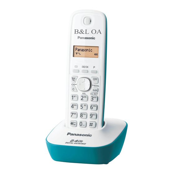
(Handset)
(Charger Unit)
Configuration for each model
Model No
Base Unit
KX-TG3411 1 (TG3411) 1 (TGA341)
KX-TG3412 1 (TG3411) 2 (TGA341)
KX-TG3419 1(TG3419) 1 (TGA341)
KX-TG3411BXC/BXH/
BXP/BXR/BXW
(Base Unit)
Handset
Charger Unit
1
Telephone Equipment
KX-TG3411BXC
Model No.
KX-TG3411BXH
KX-TG3411BXP
KX-TG3411BXR
KX-TG3411BXW
KX-TG3412BXC
KX-TG3412BXH
KX-TG3412BXP
KX-TG3412BXR
KX-TG3412BXW
KX-TG3419BXH
KX-TGA341BXC
KX-TGA341BXH
KX-TGA341BXP
KX-TGA341BXR
KX-TGA341BXW
2.4 GHz Digital Cordless Phone Solution
C: Aqua Version
H: Charcoal Gray Version
P: Pink Version
R: Red Version
W: White Version
(for Asia, Middle Near East and Other areas)
© Panasonic System Networks Co., Ltd. 2011
Unauthorized copying and distribution is a violation
of law.
ORDER NO. KM41105382CE
Advertisement
Table of Contents


Need help?
Do you have a question about the KX-TG3411BXH and is the answer not in the manual?
Questions and answers