Table of Contents
Advertisement
SERVICE MANUAL
MDS-SD1 is the minidisc deck that can
be used only with section CMT-SD1/SD3.
US and foreign patents licensed from Dolby Laboratories
Licensing Corporation.
MICROFILM
MDS-SD1
Model Name Using Similar Mechanism
MD Mechanism Type
Base Unit Type
Optical Pick-up Type
SPECIFICATIONS
– 1 –
AEP Model
UK Model
E Model
MDS-JE520
MDM-5A
MBU-5A
KMS-260A/J1N
MINIDISC DECK
Advertisement
Table of Contents

Related Manuals for Sony MDS-SD1


Summary of Contents for Sony MDS-SD1
- Page 1 MDS-SD1 SERVICE MANUAL AEP Model UK Model E Model MDS-SD1 is the minidisc deck that can be used only with section CMT-SD1/SD3. US and foreign patents licensed from Dolby Laboratories Model Name Using Similar Mechanism MDS-JE520 Licensing Corporation. MD Mechanism Type...
- Page 2 SELF-DIAGNOSIS FUNCTION The self-diagnosis function consists of error codes for customers which are displayed automatically when errors occur, and error codes which show the error history in the test mode during servicing. For details on how to view error codes for the customer, refer to the following box in the instruction manual.
- Page 3 ITEMS OF ERROR HISTORY MODE ITEMS AND CONTENTS Selecting the Test Mode Display Details of History Displays the recording time. total rec Displayed as “rππππππh”. The displayed time is the total time the laser is set to the high power state. This is about 1/4 of the actual recording time.
- Page 4 WITH MARK ! ON THE SCHEMATIC DIAGRAMS AND IN : Hong Kong model : Singapore model THE PARTS LIST ARE CRITICAL TO SAFE OPERATION. REPLACE THESE COMPONENTS WITH SONY PARTS WHOSE PART NUMBERS APPEAR AS SHOWN IN THIS MANUAL OR IN SUPPLEMENTS PUBLISHED BY SONY. – 4 –...
-
Page 5: Table Of Contents
TABLE OF CONTENTS 1. SERVICING NOTE ............6 2. GENERAL ................ 15 3. DISASSEMBLY 3-1. Glass ASSY ................. 16 3-2. Front Panel ................. 16 3-3. Slider (CAM) ..............17 3-4. Base Unit and BD Board ............ 17 3-5. SW Board and Loading Motor (M103) ......18 4. -
Page 6: Servicing Note
SECTION 1 SERVICING NOTE JIG FOR CHECKING BD BOARD WAVEFORM The special jig (J-2501-149-A) is useful for checking the waveform of the BD board. The names of terminals and the checking items to be performed are shown as follows. GND : Ground I+3V : For measuring IOP (Check the deterioration of the optical pick-up laser) IOP : For measuring IOP (Check the deterioration of the optical pick-up laser) TEO : TRK error signal (Traverse adjustment) - Page 7 IOP DATA RECORDING AND DISPLAY WHEN PICKUP AND NON-VOLATILE MEMORY (IC171 OF BD BOARD) ARE REPLACED The IOP value labeled on the pick-up can be recorded in the non-volatile memory. By recording the value, it will eliminate the need to look at the value on the label of the optical pick-up.
- Page 8 CHECKS PRIOR TO PARTS REPLACEMENT AND ADJUSTMENTS Before performing repairs, perform the following checks to determine the faulty locations up to a certain extent. Details of the procedures are described in “5 Electrical Adjustments”. Criteria for Determination Measure if unsatisfactory: (Unsatisfactory if specified value is not satisfied) Laser power check •...
- Page 9 FORCED RESET The system microprocessor can be reset in the following procedure. Use these procedure when the unit cannot be operated normally due to the overrunning of the microprocessor, etc. Procedure : Short-circuit jumper wire of JW40 and JW41 (RESET). [MAIN BOARD] (Component Side) JW40 IC821...
- Page 10 CLEANING OF OBJECTIVE LENS OF OPTICAL PICKUP • When cleaning the objective lens of the optical pickup, move the mechanism deck using the following method. 1 If a disc is inside, eject it out. 2 Disconnect the power cord from the outlet, and set the non-conducted state. 3 Using a pair of tweezers, while pulling the claw at A towards B, move part C in direction D.
- Page 11 ATTACHING THE GLASS ASSEMBLY • Attach according to steps 1 to 4. 4 Screw (PTP2.6x6) 3 Bracket (shaft) (Bottom side) When fixing this part, secure at the center to allow for some play. Open and close the glass window several times, and check that the parts do not touch each other.
- Page 12 SERVICING POSITION 1 Remove the four screws securing the upper cover, and remove the upper cover. 2 Undo the bound cables. 3 Remove the two screws A securing the rear panel. 4 Remove the four screws B securing the transformer. 5 Remove the screw C securing the MAIN board.
- Page 13 RETRY CAUSE DISPLAY MODE • In this test mode, the causes for retry of the unit during recording can be displayed on the fluorescent indicator tube. During playback, the “track mode” for obtaining track information will be set. This is useful for locating the faulty part of the unit. •...
- Page 14 Reading the Track Mode Display Higher Bits Lower Bits Details Hexa- Hexadecimal decimal b7 b6 b5 b4 b3 b2 b1 b0 When 0 When 1 Binary Emphasis ON Emphasis OFF Stereo Monaural This is 2-bit display. Normally 01. 01:Normal audio. Others:Invalid Invalid Audio (Normal) Digital copy...
-
Page 15: General
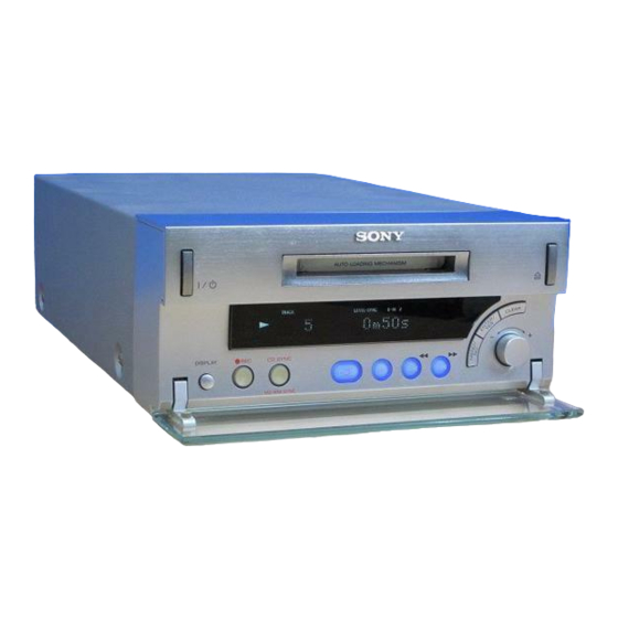
SECTION 2 GENERAL Front Panel Location of Parts and Controls 1 1/u (Power) button 9 ≠/0 button 10 π button 2 MD disk compartment 3 § button 11 fl button 12 CD SYNC/MD WM SYNC button 4 CLEAR button 13 r REC button 5 ENTER/YES button 6 VOLUME knob 14 DISPLAY button... -
Page 16: Disassembly
SECTION 3 DISASSEMBLY Note: Follow the disassembly procedure in the numerical order given. 3-1. GLASS ASSY 1 Screw (PTP2.6x6) 2 Bracket (shaft) (Bottom side) 3-2. FRONT PANEL 3 Flat type wire (13core) (CN791) 2 Connector (CN792) 4 Connector (CN793) 5 Front panel 1 Two screws (BVTP3x8) –... -
Page 17: Slider (Cam)
3-3. SLIDER (CAM) 6 Slider (Cam) Set the shaft of Cam gear to be at the position in the figure. 2 Bracket (Guide L) 1 Two screws (BTP2.6x6) Set the shaft of Lever (O/C) to 3 Leaf spring be at the position in the figure. 4 Two screws (BTP2.6x6) 5 Bracket (Guide R) 3-4. -
Page 18: Sw Board And Loading Motor (M103)
3-5. SW BOARD AND LOADING MOTOR (M103) 1 Screw (PTPWH M2.6x6) 2 Gear B 3 Two screws (PWH1.7x4) 4 Loading motor (M103) 6 SW board 5 Two screws (BTP2.6x6) – 18 –... -
Page 19: Test Mode
SECTION 4 TEST MODE 4-1. PRECAUTIONS FOR USE OF TEST MODE • As loading related operations will be performed regardless of the test mode operations being performed, be sure to check that the disc is stopped before setting and removing it. Even if the §... - Page 20 4-5. SELECTING THE TEST MODE There are 31 types of test modes as shown below. The groups can be switched by rotating the – ˜ + knob. After selecting the group to be used, press the ENTER/YES button. After setting a certain group, rotating the – ˜ + knob switches between these modes. Refer to “Group”...
-
Page 21: Functions Of Other Buttons
4-5-1. Operating the Continuous Playback Mode 1. Entering the continuous playback mode 1 Set the disc in the unit. (Whichever recordable discs or discs for playback only are available.) 2 Rotate the – ˜ + knob and display “CPLAY MODE”. 3 Press the ENTER/YES button to change the display to “CPLAY MID”. - Page 22 4-7. TEST MODE DISPLAYS Each time the DISPLAY button is pressed, the display changes in the following order. 1. Mode display Displays “TEMP ADJUST”, “CPLAYMODE”, etc. Mode display 2. Error rate display Error rate display Displays the error rate in the following way. C1 = AD = Address display...
-
Page 23: Electrical Adjustments
SECTION 5 ELECTRICAL ADJUSTMENTS 5-1. PARTS REPLACEMENT AND ADJUSTMENT • Check and adjust the MDM and MBU as follows. The procedure changes according to the part replaced • Abbreviation : Optical pick-up OWH: Overwrite head • Temperature compensation offset check •... - Page 24 5-2. PRECAUTIONS FOR CHECKING LASER DIODE 4) Use the following tools and measuring devices. • Check Disc (MD) TDYS-1 EMISSINON (Parts No. 4-963-646-01) To check the emission of the laser diode during adjustments, never • Test Disk (MDW-74/AU-1) (Parts No. 8-892-341-41) view directly from the top as this may lose your eye-sight.
- Page 25 5-6. CHECKS PRIOR TO REPAIRS Note 1: After step 4, each time the ENTER/YES button is pressed, the display will be switched between “LD 0.7 mW $ ”, These checks are performed before replacing parts according to “LD 6.2 mW $ ”, and “LD Wp ”.
- Page 26 5-6-4. Focus Bias Check 10. Observe the waveform of the oscilloscope, and check that the specified value is satisfied. Do not rotate the – ˜ + knob. Change the focus bias and check the focus tolerance amount. Checking Procedure : (Traverse Waveform) 1.
- Page 27 5-7. INITIAL SETTING OF ADJUSTMENT VALUE 5-9. TEMPERATURE COMPENSATION OFFSET ADJUTMENT Note: Save the temperature data at that time in the non-volatile memory Mode which sets the adjustment results recorded in the non-volatile as 25 ˚C reference data. memory to the initial setting value. However the results of the Note : temperature compensation offset adjustment will not change to the 1.
- Page 28 7. Then, rotate the – ˜ + knob and display “LDPWR CHECK”. 5-11. TRAVERSE ADJUSTMENT 8. Press the ENTER/YES button once and display “LD 0.9 mW $ Connection : ”. Check that the reading of the laser power meter become Oscilloscope 0.85 to 0.91 mW.
- Page 29 11. Rotate the – ˜ + knob until the waveform of the oscillo- 5-12. FOCUS BIAS ADJUSTMENT scope moves closer to the specified value. Adjusting Procedure : In this adjustment, waveform varies at intervals of approx. 2%. 1. Load a test disk (MDW-74/AU-1). Adjust the waveform so that the specified value is satisfied as 2.
- Page 30 5-13. ERROR RATE CHECK 5-15. AUTO GAIN CONTROL OUTPUT LEVEL 5-13-1. CD Error Rate Check ADJUSTMENT Checking Procedure : Be sure to perform this adjustment when the pickup is replaced. 1. Load a check disc (MD) TDYS-1. If the adjustment results becomes “Adjust NG!”, the pickup may be 2.
- Page 31 5-15. ADJUSTING POINTS AND CONNECTING POINTS [BD BOARD] (SIDE A) CN101 D101 CN110 I+3V NOTE IC171 [BD BOARD] (SIDE B) IC101 IC121 IC192 NOTE:It is useful to use the jig. for checking the waveform. (Refer to Servicing Note on page 6.) –...
-
Page 32: Diagrams
SECTION 6 DIAGRAMS 6-1. CIRCUIT BOARDS LOCATION MAIN board CONNECTOR board SW board PANEL SW board BD board PANEL board ENCODER board – 32 –... -
Page 33: Block Diagrams
MDS-SD1 DIGITAL SERVO SIGNAL PROCESSOR, DIGITAL SIGNAL PROCESSOR 6-2. BLOCK DIAGRAMS EFM/ACIRC ENCODER/DECODER, SHOCK-PROOF MEMORY CONTROLLER, ATRAC ENCODER/DECODER – BD SECTION – IC121 OVER WRITE HEAD DRIVE IC181 SCTX DIG-RST HR901 OVER WRITE DIN0 • HEAD DIN0 • HEAD DIN1... -
Page 34: Main Section
MDS-SD1 – MAIN SECTION – IC601 OPT IN 1 CS/BS A/D,D/A CONVERTER IC502 IC201 J101 IC601 OPT IN 1 CD DATAO VINL1 DIGITAL IC501 DIN0 VINL2 OPTICAL R-CH LINE AMP VINR1 DIN1 R-CH IC101 OPT OUT VINR2 DOUT IC503 VOUTL... - Page 35 MDS-SD1 WAVEFORMS THIS NOTE IS COMMON FOR PRINTED WIRING – BD (1/2) SECTION – – MAIN SECTION – BOARDS AND SCHEMATIC DIAGRAMS. (In addition to this, the necessary note is printed in each block.) 0.46Vp-p 3.2Vp-p For schematic diagrams. Note: 10MHz •...
-
Page 36: Printed Wiring Board - Bd Section
MDS-SD1 6-3. PRINTED WIRING BOARD – BD SECTION – • See page 32 for Circuit Boards Location. (Page 49) (Page 49) • Semiconductor • Semiconductor Location Location Ref. No. Location Ref. No. Location D101 D181 IC101 D183 IC121 IC124 IC103... -
Page 37: Schematic Diagram - Bd (1/2) Section
MDS-SD1 6-4. SCHEMATIC DIAGRAM – BD (1/2) SECTION – • See page 38 for Waveforms. • See page 61 for IC Block Diagrams. • See page 64 for IC Pin Functions. RT1P441M-TP-1 RT1P441M- TP-1 RT1P441M-TP-1 RT1P441M-TP-1 (Page 43) (Page 44) -
Page 38: Schematic Diagram - Bd (2/2) Section
MDS-SD1 6-5. SCHEMATIC DIAGRAM – BD (2/2) SECTION – • See page 38 for Waveforms. • See page 39 for Printed Wiring Board. (Page 41) (Page 41) (Page 42) (Page 42) (Page 42) (Page 41) (Page 42) (Page 45) (Page 45) S-24CO2AFJA-TB –... -
Page 39: Schematic Diagram - Main (1/2) Section
MDS-SD1 6-6. SCHEMATIC DIAGRAM – MAIN (1/2) SECTION – • See page 38 for Waveforms. • See page 49 for Printed Wiring Board. • See page 65 for IC Pin Functions. (Page 59) (Page 43) (Page 55, 56) (Page 43) -
Page 40: Schematic Diagram - Main (2/2) Section
MDS-SD1 6-7. SCHEMATIC DIAGRAM – MAIN (2/2) SECTION – • See page 38 for Waveforms. • See page 62 for IC Block Diagrams. (Page 45) (Page 46) (Page 45) (Page 52) – 47 – – 48 –... -
Page 41: Printed Wiring Board - Main Section
MDS-SD1 6-8. PRINTED WIRING BOARD – MAIN SECTION – • Semiconductor Location • See page 32 for Circuit Boards Location. Ref. No. Location D172 D173 D811 D812 DIGITAL OPTICAL D815 D816 D821 D823 D824 D831 D832 D833 D851 D852 D861... -
Page 42: Schematic Diagram - Panel Section
MDS-SD1 6-9. SCHEMATIC DIAGRAM – PANEL SECTION – • See page 38 for Waveforms. 470p DTC144EKA-T146 DTC144EKA-T146 DTC143TKA-T146 (Page 47) – 51 – – 52 –... -
Page 43: Printed Wiring Board - Panel Section
MDS-SD1 6-10. PRINTED WIRING BOARD – PANEL SECTION – • See page 32 for Circuit Boards Location. (Page 49) • Semiconductor Location Ref. No. Location D941 D942 D943 D944 D945 D946 IC901 Q921 Q941 Q942 – 53 – – 54 –... -
Page 44: Schematic Diagram - Connector Section
MDS-SD1 6-11. SCHEMATIC DIAGRAM – CONNECTOR SECTION – • See page 63 for IC Block Diagrams. (Page 46) – 55 – – 56 –... -
Page 45: Printed Wiring Board - Connector Section
MDS-SD1 6-12. PRINTED WIRING BOARD – CONNECTOR SECTION – • See page 32 for Circuit Boards Location. • Semiconductor Location SYSTEM CONTROL Ref. No. Location D781 CONTROL TO HCD-SD1 TO TC-SD1 D782 IC771 IC772 IC774 Q771 Q772 Q774 Q775 Q781... -
Page 46: Schematic Diagram - Bd Switch Section
MDS-SD1 6-15. SCHEMATIC DIAGRAM – ENCODER SECTION – 6-13. SCHEMATIC DIAGRAM – BD SWITCH SECTION – (Page 45) (Page 45) 6-14. PRINTED WIRING BOARD – BD SWITCH SECTION – 6-16. PRINTED WIRING BOARD – ENCODER SECTION – • See page 32 for Circuit Boards Location. -
Page 47: Ic Block Diagrams
6-17. IC BLOCK DIAGRAMS – BD Section – IC101 CXA2523AR 43 42 USROP – RF AGC – USRC RFA1 BPF3T RFA2 PEAK3T – HLPT –1 – – –2 – CFST PTGR TEMP PEAK – –2 – BOTTOM 36 BOTM – –1 GRVA 35 ABCD... -
Page 48: Main Section
IC152 BH6511FS-E2 INTERFACE INTERFACE CHARGE PREDRIVE PREDRIVE PUMP. PREDRIVE PREDRIVE INTERFACE INTERFACE – MAIN Section – IC201 UDA1341TS/N2 IC301 LB1641 T.S.D O.C.P MOTOR MOTOR VINL2 VINR2 DRIVE DRIVE 0DB/6DB 0DB/6DB ADC2R ADC2L VINR1 VINL1 SWITCH SWITCH ADC1L ADC1R AGCSTAT FWD/REV/STOP VDDD DIGITAL AGC CONTROL LOGIC... - Page 49 IC822 M62016FP-E1 INTERRUPT SIGNAL – GENERATOR RESET SIGNAL 1 RESET – GENERATOR IC851 M5293L REFERENCE VOLTAGE REFERENCE – ON/OFF VOLTAGE OVERHEAT OVERCURRENT PROTECTION LIMITTER – CONNECTOR Section – IC774 P82B715TD.118 BUFFER BUFFER – 63 –...
-
Page 50: Ic Pin Functions
6-18. IC PIN FUNCTIONS • IC101 CXA2523AR (RF Amplifier) (BD Board) Pin No. Pin Name Function I-V converted RF signal I input from the optical pick-up block detector I-V converted RF signal J input from the optical pick-up block detector Middle point voltage (+1.65V) generation output terminal 4 to 9 A to F... - Page 51 • IC701 M30610MC-A01FP (SYSTEM CONTROL µCON) (MAIN BOARD) Pin Name Function Pin No. WMOUT MD WM LINK data out WMCLK MD WM LINK clock in LEVEL-L LEVEL-L DA output (Not used) LEVEL-R LEVEL-R DA output (Not used) LEDDATA LED DRIVER DATA output (Not used) Not used LEDCLK LED DRIVER CLOCK output (Not used)
- Page 52 Pin Name Function Pin No. CHAK-IN Detection signal from IN switch HOME Detection signal form HOME switch PACK-OUT Detection signal from OUT switch LDIN Loading motor in control LDOUT Loading motor out control LD-LOW Loading motor voltage control output LDON Laser power ON/OFF REFLECT Disc reflection rate detection...
-
Page 53: Exploded Views
SECTION 7 EXPLODED VIEWS NOTE: The components identified by • Hardware (# mark) list and accessories and pack- • Items marked “*” are not stocked since they are mark ! or dotted line with mark ing materials are given in the last of this parts list. seldom required for routine service. -
Page 54: Front Panel Section
4-212-584-01 BRACKET (SHAFT) * 62 1-671-539-11 PANEL SW BOARD 4-993-007-01 SCREW (M2.6X6), +P TAPPING X-4950-998-1 BRACKET (L) ASSY 4-942-636-21 EMBLEM (NO.3.5), SONY 4-996-690-91 LID (CARTRIDGE) 4-212-551-11 PANEL (AL-MD), FRONT 4-976-593-01 SPRING (LID), TORSION X-4950-996-1 PANEL (MD) ASSY , FRONT 1-751-086-11 WIRE (FLAT TYPE) (13 CORE) -
Page 55: Mechanism Section (Mdm-5A)
7-3. MECHANISM DECK SECTION (MDM-5A) M103 MBU-5A Ref. No. Part No. Description Remark Ref. No. Part No. Description Remark 4-996-227-01 LEVER (HEAD) * 201 1-671-115-21 SW BOARD * 202 4-996-217-01 CHASSIS 4-996-229-01 SPRING (HEAD LEVER), TORSION 4-996-223-11 INSULATOR (F) 4-996-212-01 LEVER (LIMITTER) * 204 4-996-218-01 BRACKET (GUIDE R) 4-996-213-01 SPRING (LIMITTER), TORSION... -
Page 56: Base Unit Section (Mbu-5A)
7-4. BASE UNIT SECTION (MBU-5A) HR901 not supplied not supplied M101 S102 M102 The components identified by mark ! or dotted line with mark ! are critical for safety. Replace only with part number specified. Ref. No. Part No. Description Remark Ref. -
Page 57: Electrical Parts List
SECTION 8 ELECTRICAL PARTS LIST Note: • SEMICONDUCTORS • Due to standardization, replacements in the parts list The components identified by In each case, u: µ , for example: may be different from the parts specified in the mark ! or dotted line with mark uA...: µ... - Page 58 CONNECTOR Ref. No. Part No. Description Remark Ref. No. Part No. Description Remark L122 1-414-813-11 FERRITE R152 1-216-073-00 METAL CHIP 1/10W L151 1-412-029-11 INDUCTOR CHIP 10uH R158 1-216-097-91 RES,CHIP 100K 1/10W L152 1-412-029-11 INDUCTOR CHIP 10uH R159 1-216-097-91 RES,CHIP 100K 1/10W L153 1-412-032-11 INDUCTOR CHIP 100uH...
- Page 59 ENCODER CONNECTOR MAIN Ref. No. Part No. Description Remark Ref. No. Part No. Description Remark C792 1-163-121-00 CERAMIC CHIP 150PF R781 1-216-073-00 METAL CHIP 1/10W < CONNECTOR > R782 1-216-073-00 METAL CHIP 1/10W R783 1-216-073-00 METAL CHIP 1/10W * CN771 1-568-832-11 SOCKET, CONNECTOR 13P R784 1-216-073-00 METAL CHIP...
- Page 60 MAIN Ref. No. Part No. Description Remark Ref. No. Part No. Description Remark C503 1-163-038-91 CERAMIC CHIP 0.1uF D812 8-719-200-82 DIODE 11ES2 C504 1-163-121-00 CERAMIC CHIP 150PF D815 8-719-016-74 DIODE 1SS352 C505 1-163-121-00 CERAMIC CHIP 150PF C506 1-163-038-91 CERAMIC CHIP 0.1uF D816 8-719-016-74 DIODE 1SS352...
- Page 61 MAIN Ref. No. Part No. Description Remark Ref. No. Part No. Description Remark < COIL > R601 1-216-089-91 RES,CHIP 1/10W R602 1-216-089-91 RES,CHIP 1/10W L501 1-414-396-21 INDUCTOR 4.7uH R605 1-216-121-91 RES,CHIP 1/10W < LINE FILTER > R606 1-216-025-91 RES,CHIP 1/10W R607 1-216-025-91 RES,CHIP 1/10W...
- Page 62 PANEL PANEL SW Ref. No. Part No. Description Remark Ref. No. Part No. Description Remark A-4724-619-A PANEL BOARD, COMPLETE R946 1-216-034-00 METAL CHIP 1/10W ********************* R947 1-216-034-00 METAL CHIP 1/10W < CAPACITOR > R948 1-216-089-91 RES,CHIP 1/10W C901 1-163-038-91 CERAMIC CHIP 0.1uF <...
- Page 63 Ref. No. Part No. Description Remark ACCESSORIES & PACKING MATERIALS ******************************* 1-543-793-11 FILTER, CLAMP (FERRITE CORE) 1-558-271-11 CORD, CONNECTION (AUDIO, 108cm) 1-574-264-11 CORD, OPTICAL PLUG (OPTICAL PLUG, 60cm) (AEP,UK) 1-790-034-11 CORD (WITH CONNECTOR) (5 CORE) (SYSTEM CABLE, 50cm) 1-790-137-11 CORD (WITH CONNECTOR) (WALKMAN-LINK, 80cm) 3-864-771-11 MANUAL, INSTRUCTION (ENGLISH) 3-864-771-21 MANUAL, INSTRUCTION...
- Page 64 MDS-SD1 Sony Corporation 98L0953-1 Printed in Japan © 1998. 12 9-922-970-11 Home A&V Products Company Published by Quality Assurance Dept. – 78 – (Shibaura)