Table of Contents
Advertisement
Advertisement
Table of Contents

Related Manuals for Philco STC-9630


Summary of Contents for Philco STC-9630
- Page 1 SERVICE MANUAL STC-9630 OPEN/CLOSE...
-
Page 2: Table Of Contents
CONTENTS SAFETY PRECAUTIONS PREVENTION OF ELECTRO STATIC DISCHARGE(ESD)TO ELECTROSTATICALLY SENSITIVE(ES)DEVICES CONTROL BUTTON LOCATIONS AND EXPLANATIONS PREVERTION OF STATIC ELECTRICITY DISCHARGE ASSEMBLING AND DISASSEMBLING THE MECHANISM UNIT OPTICAL PICKUP UNIT EXPLOSED VIEW AND PART LIST BRACKET EXPLOSED VIEW AND PART LIST MISCELLANEOUS ELECTRICAL CONFIRMATION VIDEO OUTPUT (LUMINANCE SIGNAL) CONFIRMATION... -
Page 3: Safety Precautions
1. SAFETY PREAUTIONS 1.1 GENERAL GUIDELINES 1. When servicing, observe the original lead dress. if a short circuit is found, replace all parts which have been overheated or damaged by the short circuit. 2. After servicing, see to it that all the protective devices such as insulation barrier, insulation papers shields are properly installed. -
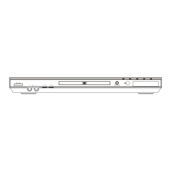
Page 4: Control Button Locations And Explanations
OPEN/CLOSE 11 12 POWER switch STOP button MIC 1 VOLUME knob Disc tray REW button MIC 2 VOLUME knob OPEN/CLOSE button FWD button IR SENSOR MIC 1 jack LED display window PLAY button MIC 2 jack PAUSE button... -
Page 5: Prevention Of Static Electricity Discharge
4.PREVENTION OF STATIC ELECTRICITY DISCHARGE The laser diode in the traverse unit (optical pickup)may brake down due to static electricity of clothes or human body. Use due caution to electrostatic breakdown when servicing and handling the laser diode. 4.1.Grounding for electrostatic breakdown prevention Some devices such as the DVD player use the optical pickup(laser diode)and the optical pickup will be damaged by static electricity in the working environment.Proceed servicing works under the working environment where grounding works is completed. -
Page 6: Assembling And Disassembling The Mechanism Unit
5. Assembling and disassembling the mechanism unit 5.1 Optical pickup Unit Explosed View and Part List Pic (1) - Page 7 Materials to Pic (1) PARTS CODE PARTS NAME Q ty 14692200 SF-HD60 1EA0311A06300 ASSY, CHASSIS, COMPLETE 1EA0M10A15500 ASSY, MOTOR, SLED 1EA0M10A15501 ASSY, MOTOR, SLED 1EA2451A24700 HOLDER, SHAFT 1EA2511A29100 GEAR, RACK 1EA2511A29200 GEAR, DRIVE 1EA2511A29300 GEAR, MIDDLE, A 1EA2511A29400 GEAR, MIDDLE, B 1EA2744A03000 SHAFT, SLIDE 1EA2744A03100...
-
Page 8: Bracket Explosed View And Part List
5.2 Bracket Explosed View and Part List Pic (2) Materials to Pic(2) 1.bracket 14. front silicon rubber 2.belt 15. Back silicon rubber 3.screw 16. Pick-up 4.belt wheel 17. Pick-up 5.gearwheel 18. switch 6.iron chip 19. Five-pin flat plug 7. Immobility mechanism equipment 20. -
Page 9: Miscellaneous
5.3 MISCELLANEOUS 5.3.1 Protection of the LD(Laser diode) Short the parts of LD circuit pattern by soldering. 5.3.2 Cautions on assembly and adjustment Make sure that the workbenches,jigs,tips,tips of soldering irons and measuring instruments are grounded,and that personnel wear wrist straps for ground. Open the LD short lands quickly with a soldering iron after a circuit is connected. -
Page 10: Electrical Confirmation
6.Electrical Confirmation 6.1. Video Output (Luminance Signal) Confirmation DO this confirmation after replacing a P.C.B. Measurement point Mode Disc Color bar 75% DVDT-S15 Video output terminal PLAY(Title 46):DVDT-S15 PLAY(Title 12):DVDT-S01 DVDT-S01 Measuring equipment,tools Confirmation value 200mV/dir,10 sec/dir 1000mVp-p±30mV Purpose:To maintain video signal output compatibility. 1.Connect the oscilloscope to the video output terminal and terminate at 75 ohms. -
Page 11: Video Output(Chrominance Signal) Confirmation
6.2 Video Output(Chrominance Signal) Confirmation Do the confirmation after replacing P.C.B. Measurement point Mode Disc Color bar 75% DVDT-S15 Video output terminal PLAY(Title 46):DVDT-S15 PLAY(Title 12):DVDT-S01 DVDT-S01 Measuring equipment,tools Confirmation value Screwdriver,Oscilloscope 200mV/dir,10 sec/dir 621mVp-p±30mV Purpose:To maintain video signal output compatibility. 1.Connect the oscilloscope to the video output terminal and terminate at 75 ohme. -
Page 12: Mpeg Board Check Waveform
7.MPEG BOARD CHECK WAVEFORM 7.1 27MHz WAVEFORM DIAGRAM 7.2 IC5L0380R PIN.2 WAVEFORM DIAGRAM... -
Page 13: Ic Block Diagram & Description
MT1336 PRELIMINARY, SUBJ ECT TO CHANGE WITHOUT NOTICE MTK CONFIDENTIAL, NO DISCLOSURE 8. IC BLOCK DIAGRAM & DESCRIPTION 8.1 MT1336 GENERAL DESCRIPTION M T 1 3 3 6 i s a h i g h p e r f o r m a n c e C M O S a n a l o g f r o n t -e n d I C f o r b o t h C D _ R O M d r i v e r u p t o 4 8 X S a n d D V D - R O M d r i v e r u p t o 1 6 X S . - Page 14 MT1336 PRELIMINARY, SUBJ ECT TO CHANGE WITHOUT NOTICE MTK CONFIDENTIAL, NO DISCLOSURE DVDA RFOP DVDB ATTENUATOR INPUT MUX RFON DVDC LRFRP DEFECT DVDD HRFRP CRTP DVDRFIN ENVELOP ENVELOP CRTPLP DETECTOR DETECTOR DVDRFIP REFCOS HALLCOS SBAD COSPHI DPFN REFSIN DPFO HALLSIN SINPHI DPDMUTE MDI2...
- Page 15 MT1336 PRELIMINARY, SUBJ ECT TO CHANGE WITHOUT NOTICE MTK CONFIDENTIAL, NO DISCLOSURE W O BSO W V D D A G N D X DVDA A G N D X DVDB A V D D O DVDC R FO P DVDD R FO N DVDRFI P...
- Page 16 MT1336 PRELIMINARY, SUBJ ECT TO CHANGE WITHOUT NOTICE MTK CONFIDENTIAL, NO DISCLOSURE MT1336 PIN DESCRIPTIONS Pin Numbers Symbol Type Description LQFP128 RF Flag Interface DEFECT Digital Output Flag of bad data output status RF SIO interface SCLK Digital Input RF serial clock input SDEN Digital Input RF serial data enable...
- Page 17 MT1336 PRELIMINARY, SUBJ ECT TO CHANGE WITHOUT NOTICE MTK CONFIDENTIAL, NO DISCLOSURE RFGCU Analog RF AGC loop capacitor connecting for DVD -RAM RFGCI Analog RF AGC loop capacitor connecting for DVD -RAM Analog Input DC coupled DVD-RAM main-beam RF signal input A Analog Input DC coupled DVD-RAM main-beam RF signal input B Analog Input...
- Page 18 MT1336 PRELIMINARY, SUBJ ECT TO CHANGE WITHOUT NOTICE MTK CONFIDENTIAL, NO DISCLOSURE Analog Input MDI1 Laser power monitor input LDO1 Analog Ou tput Laser driver output Analog Input MDI2 Laser power monitor input LDO2 Analog Output Laser driver output RF RIPPLE CRTP Analog RF top envelop filter capacitor connecting...
- Page 19 MT1336 PRELIMINARY, SUBJ ECT TO CHANGE WITHOUT NOTICE MTK CONFIDENTIAL, NO DISCLOSURE ALPC TRIMMING Analog input Trimming pin for ALPC1 Analog input Trimming pin for ALPC1 Analog input Trimming pin for ALPC2 Analog input Trimming pin for ALPC2 HIGH SPEED TRACK COUNTING TRLP Analog Low-pass filter capacitor connecting...
- Page 20 MT1336 PRELIMINARY, SUBJ ECT TO CHANGE WITHOUT NOTICE MTK CONFIDENTIAL, NO DISCLOSURE...
-
Page 21: Mt1379
MT1379 Progressive Scan DVD Player Combo Chip Speci f i c ati o ns are subj e ct to change wi t hout noti c e 8.2 MT1379 § Tray control can be PWM output or digital output Super Integration DVD player single chip §... - Page 22 MT1379 PRELIMINARY, SUBJECT TO CHANGE WITHOUT NOTICE MTK CONFIDENTIAL, NO DISCLOSURE § cycle timings Downmix function § § Block-based sector addressing Support IEC 60958/61937 output § Programmable buffering counter for buffer status - PCM / bit stream / mute mode tracking - Custom IEC latency up to 2 frames §...
- Page 23 MT1379 PRELIMINARY, SUBJECT TO CHANGE WITHOUT NOTICE MTK CONFIDENTIAL, NO DISCLOSURE EFINITIONS Pin Number Symbol Type Description IREF Analog Input Current reference input. It generates reference current for data PLL. Connect an ext ernal 100K resistor to this pin and PLLVSS. PLLVSS Ground Ground pin for data PLL and related analog circuitry...
- Page 24 MT1379 PRELIMINARY, SUBJECT TO CHANGE WITHOUT NOTICE MTK CONFIDENTIAL, NO DISCLOSURE Pin Number Symbol Type Description HIGHA6 Inout Microcontroller address 14 2~16MA, SR HIGHA7 Inout Microcontroller address 15 2~16MA, SR Inout Microcontroller address/data 7 2~16MA, SR Inout Microcontroller address/data 6 2~16MA, SR Inout Microcontroller address/data 5...
- Page 25 MT1379 PRELIMINARY, SUBJECT TO CHANGE WITHOUT NOTICE MTK CONFIDENTIAL, NO DISCLOSURE Pin Number Symbol Type Description IOA7 Inout Microcontroller address 7 / IO 2~16MA, SR Output Flash address 16 2~16MA, SR Output Flash address 17 2~16MA, SR IOA18 Inout Flash address 18 / IO 2~16MA, SR IOA19 Inout...
- Page 26 MT1379 PRELIMINARY, SUBJECT TO CHANGE WITHOUT NOTICE MTK CONFIDENTIAL, NO DISCLOSURE Pin Number Symbol Type Description UP1_7 Inout Microcontroller port 1 -7 4MA, SR PU, SMT UP3_0 Inout Microcontroller port 3 -0 4MA, SR PU, SMT UP3_1 Inout Microcontroller port 3 -1 4MA, SR PU, SMT INT0#...
- Page 27 MT1379 PRELIMINARY, SUBJECT TO CHANGE WITHOUT NOTICE MTK CONFIDENTIAL, NO DISCLOSURE Pin Number Symbol Type Description RD14 Inout DRAM data 14 2~16MA, SR PU/PD, SMT RD13 Inout DRAM data 13 2~16MA, SR PU/PD, SMT RD12 Inout DRAM data 12 2~16MA, SR PU/PD, SMT DVDD3 Power...
- Page 28 MT1379 PRELIMINARY, SUBJECT TO CHANGE WITHOUT NOTICE MTK CONFIDENTIAL, NO DISCLOSURE Pin Number Symbol Type Description DQM0 Output Mask for DRAM input/output byte 0 2~16MA, SR Output DRAM bank address 0 2~16MA, SR RA10 Output DRAM address10 2~16MA, SR DVDD2 Power 2.5V power pin for internal digital circuitry Output...
- Page 29 MT1379 PRELIMINARY, SUBJECT TO CHANGE WITHOUT NOTICE MTK CONFIDENTIAL, NO DISCLOSURE Pin Number Symbol Type Description RD23 Inout DRAM data 23 / 2~16MA, SR Videoin Data PortA 7 PU/PD, SMT RD22 Inout DRAM data 22 / 2~16MA, SR Videoin Data PortA 6 PU/PD, SMT DVDD2 Power...
- Page 30 MT1379 PRELIMINARY, SUBJECT TO CHANGE WITHOUT NOTICE MTK CONFIDENTIAL, NO DISCLOSURE Pin Number Symbol Type Description ASDATA3 Inout Audio serial data 3 (surround left/surround right channel) Trap value in power-on reset : PD SMT 1 : manufactory test mode 0 : normal operation OR Videoin Data PortB 1 ASDATA4 Inout...
- Page 31 MT1379 PRELIMINARY, SUBJECT TO CHANGE WITHOUT NOTICE MTK CONFIDENTIAL, NO DISCLOSURE Pin Number Symbol Type Description SPDATA Input Audio data of SPDIF input / Videoin Data PortB 5 DVDD2 Power 2.5V power pin for internal digital circuitry SPLRCK Input Audio left/right channel clock of SPDIF input / Videoin Data PortB 6 SPBCK Input...
- Page 32 MT1379 PRELIMINARY, SUBJECT TO CHANGE WITHOUT NOTICE MTK CONFIDENTIAL, NO DISCLOSURE 26 Jul, 2002 Page 1 of 2 IREF YUV0/CIN PLLVSS LPIOP VREF LPION DACVDDC LPFON ASDATA4 LPFIP ASDATA3 LPFIN ASDATA2 LPFOP ASDATA1 JITFO ASDATA0 JITFN SPDIF PLLVDD3 MC_DATA ACLK DVDD3 TROPENPWM ALRCK...
- Page 33 MT1379 PRELIMINARY, SUBJECT TO CHANGE WITHOUT NOTICE MTK CONFIDENTIAL, NO DISCLOSURE UNCTIONAL LOCK D V D m o d u l e S e r v o A n a l o g S p i n d l e D e b u g S y s t e m T V e n c o d e r...
- Page 34 MT1379 PRELIMINARY, SUBJECT TO CHANGE WITHOUT NOTICE MTK CONFIDENTIAL, NO DISCLOSURE controller changes the mode and speed of operation according to servo register setting. The PWM generator generates pulse -width-modulated signal to drive disc spindle motor driver. CSS/CPPM The CSS/CPPM module provides functions necessary for decoding discs conforming to CSS/CPPM specification. System Parser The system parser is used to help the system controller to decode DVD/SVCD/VCD bitstream just after the channel decoder performing error correction.
- Page 35 MT1379 PRELIMINARY, SUBJECT TO CHANGE WITHOUT NOTICE MTK CONFIDENTIAL, NO DISCLOSURE This is a hardware sub-picture decoder. It decodes the compressed SPU image bitstream and CHG_COLCON commands according to SPU header information previously decoded by system controller. The SPU module also allows two SPU objects to be displayed at the same time.
- Page 36 MT1379 PRELIMINARY, SUBJECT TO CHANGE WITHOUT NOTICE MTK CONFIDENTIAL, NO DISCLOSURE LECTRICAL HARACTERISTICS Absolute Maximum Rating Symbol Parameters Value Unit VDD3 3.3V Supply voltage -0.3 to 3.6 VDD2 2.5V Supply voltage -0.3 to 3.0 VDDA Analog Supply voltage -0.3 to 3.6 Input Voltage -0.3 to 5.5 Output Voltage...
-
Page 37: Am29Lv160D
8.3 Am29LV160D 16 Megabit (2 M x 8-Bit/1 M x 16-Bit) CMOS 3.0 Volt-only Boot Sector Flash Memory DISTINCTIVE CHARACTERISTICS Single power supply operation Embedded Algorithms — Full voltage range: 2.7 to 3.6 volt read and write — Embedded Erase algorithm automatically operations for battery-powered applications preprograms and erases the entire chip or any combination of designated sectors... -
Page 38: Block Diagram
PRODUCT SELECTOR GUIDE Family Part Number Am29LV160D Speed Option Voltage Range: V = 2.7–3.6 V -120 Max access time, ns (t Max CE# access time, ns (t Max OE# access time, ns (t Note: See “AC Characteristics” for full specifications. BLOCK DIAGRAM –... - Page 39 CONNECTION DIAGRAMS BYTE# DQ15/A-1 DQ14 DQ13 DQ12 Standard TSOP RESET# DQ11 RY/BY# DQ10 BYTE# DQ15/A-1 DQ14 DQ13 DQ12 RESET# Reverse TSOP DQ11 RY/BY# DQ10...
- Page 40 CONNECTION DIAGRAMS RESET# BYTE# DQ15/A-1 DQ14 DQ13 DQ10 DQ12 DQ11 FBGA Top View, Balls Facing Down BYTE# DQ15/A-1 DQ14 DQ13 RESET# DQ12 RY/BY# DQ10 DQ11 Special Handling Instructions Flash memory devices in FBGA packages may be damaged if exposed to ultrasonic cleaning methods. Special handling is required for Flash Memory products The package and/or data integrity may be compromised in FBGA packages.
- Page 41 PIN CONFIGURATION LOGIC SYMBOL A0–A19 = 20 addresses DQ0–DQ14 = 15 data inputs/outputs A0–A19 16 or 8 DQ15/A-1 = DQ15 (data input/output, word mode), DQ0–DQ15 A-1 (LSB address input, byte mode) (A-1) BYTE# = Selects 8-bit or 16-bit mode = Chip enable = Output enable = Write enable RESET#...
-
Page 42: Hy57V641620Hg
HY57V641620HG 4 Banks x 1M x 16Bit Synchronous DRAM 8.4 HY57V641620HG DESCRIPTION The Hyundai HY57V641620HG is a 67,108,864-bit CMOS Synchronous DRAM, ideally suited for the main memory applications which require large memory density and high bandwidth. HY57V641620HG is organized as 4banks of 1,048,576x16. HY57V641620HG is offering fully synchronous operation referenced to a positive edge of the clock. - Page 43 HY57V641620HG PIN CONFIGURATION DQ15 DQ14 DQ13 DQ12 DQ11 DQ10 54pin TSOP II 400mil x 875mil 0.8mm pin pitch LDQM UDQM /CAS /RAS A10/AP PIN DESCRIPTION PIN NAME DESCRIPTION The system clock input. All other inputs are registered to the SDRAM on the Clock rising edge of CLK Controls internal clock signal and when deactivated, the SDRAM will be one...
-
Page 44: Functional Block Diagram
HY57V641620HG FUNCTIONAL BLOCK DIAGRAM 1Mbit x 4banks x 16 I/O Synchronous DRAM Self refresh logic Internal Row & timer counter 1Mx16 Bank 3 1Mx16 Bank 2 Row active Decoders 1Mx16 Bank 1 1Mx16 Bank 0 Memory refresh Cell Array Column Column Active UDQM... -
Page 45: Schematic & Pcb Wiring Diagram
9. SCHEMATIC & PCB WIRING DIAGRAM FRONT SCHEMATIC DIAGRAM... - Page 46 FRONT SCHEMATIC DIAGRAM...
- Page 47 POWER BOARD SCHEMATIC DIAGRAM...
- Page 48 POWER BOARD SCHEMATIC DIAGRAM...
- Page 49 OK SCHEMATIC DIAGRAM...
- Page 50 OK SCHEMATIC DIAGRAM...
- Page 51 OUTPUT BOARD SCHEMATIC DIAGRAM...
- Page 52 OUTPUT BOARD SCHEMATIC DIAGRAM...
- Page 53 MIAN SCHEMATIC DIAGRAM...
- Page 54 MIAN SCHEMATIC DIAGRAM...
- Page 55 MIAN SCHEMATIC DIAGRAM...
- Page 56 MIAN SCHEMATIC DIAGRAM...
- Page 57 MIAN SCHEMATIC DIAGRAM...
-
Page 58: Spare Parts List
10. SPARE PARTS LIST STC-9630 MATERIAL LIST 1. DECODE BOARD MATERIAL SPECIFICATIONS/PART NUMBER LOCATION QUANTITY C2119,C2128,C2131,L243~L248,R205,R SMD RESISTOR 1/16W 0Ω ±5% 219,R220,R226,R240,R241,R244,R255,R 257,R259,R282,R332,R337,R2162,R297 SMD RESISTOR 1/16W 75Ω ±5% R256 CARBON FILM RESISTOR 1/4W2.2Ω±5% R341 SMD RESISTOR 1/16W1Ω±5% R312,R313,R317,R318,R336 SMD RESISTOR 1/16W 4.7Ω... - Page 59 C225,C241,C242,C243,C254,C256,C257, SMD CAPACITOR 50V 47P ±5% NPO 0603 C259,C260,C262,C266,C268,C269,C271 C216,C273,C274,C342,C2111,C2114,C2 SMD CAPACITOR 50V 101 ±5% NPO 0603 117,C2120,C2123,C2126 SMD CAPACITOR 50V 331 ±5% NPO 0603 C217,C218 SMD CAPACITOR 50V 151 ±5% NPO 0603 C331,C334 SMD CAPACITOR 50V 471 ±5% NPO 0603 C311 SMD CAPACITOR 50V 82P ±5% NPO 0603...
- Page 60 SMD TRIODE 3904 V305 SMD TRIODE 9014C V310 SMD TRIODE 2SK3018 V303,V304 SMD TRIODE 2SB1132 V301,V302 NJM4558M SOP U219,U220,U221 64.1 IC 4580 SOP U219,U220,U221 64.2 IC 4558 SOP U219,U220,U221 MM74HCU04M SOP U205 65.1 IC HCU04 SOP U205 HY57V641620HGT-7 TSOP U211 66.1 IC MT48LC4M16A2-7 SOP U211...
- Page 61 15.1 CERAMIC CAPACITOR CT81 400V221±10% 10mm BC503 TERYLENE CAPACITOR 100V 223 ±10% 5mm C506 TERYLENE CAPACITOR 275V 104 ±20% 15mm BC501 17.1 TERYLENE CAPACITOR 275V 104 ±10% 15mm BC501 GZ16V100U±20%6×12 2.5 TC508,TC513 18.1 CD CD11 16V100U±20%6×12 2.5 TC508,TC513 18.2 CD CD110 16V100U±20%6×12 2.5 TC508,TC513 18.3 CD...
- Page 62 FUSE HOLDER BLX-2 FOR F501 HEAT RADIATOR BOARD 11×15×25 AB009K U501,U504 FOR HEAT RADIATION 48.1 HEAT RADIATOR BOARD 11×15×25 WHITE AB905 U501,U504 FOR HEAT RADIATION AB903 G501~G502 GROUND CHIP OF POWER BOARD TAPPING SCREW BT 3×8 BLACK FIXED HEAT RADIATION BOARD 3.
- Page 63 ROTATED POTENTIOMETER WHE101N-2-B10K±20% VRB02 ROTATED POTENTIOMETER WHE101N-2-B50K±20% VRB01 5P100 2.0 2 SOCKET WITH L FLAT CABLE XSB01 NEEDLE REVERSE B963A-1 5. AV BOARD MATERIAL SPECIFICATIONS/PART NUMBER LOCATION QUANTITY CARBON FILM RESISTOR 1/4W100Ω±5% R702 CARBON FILM RESISTOR 1/4W68Ω±5% R703 CARBON FILM RESISTOR 1/4W2.2Ω±5% R706 CARBON FILM RESISTOR...
- Page 64 PT6961 SOP U401 SOCKET 2P 2.0mm XS403 SOCKET 9P 2.0mm XS402 SOCKET 6P 2.0mm XS401 SMD RESISTOR 1/16W 100Ω ±5% R412 SMD RESISTOR 1/16W 2.2Ω ±5% R408 SMD RESISTOR 1/16W 10K ±5% R403,R404,R405 SMD RESISTOR 1/16W 51K ±5% R401 SMD CAPACITOR 50V 104 +80%-20% 0603 C401 4963-2...
- Page 65 ENGLISH STC-9630 Service manual...
- Page 66 STC-9630 SERVICE MANUAL CAUTIONS There is high voltage inside this unit. Make sure to pull out the plug of this unit before repairing! There are many high voltage components inside this unit. Please pay attention to all warnings and instructions marked on this unit to avoid electric shock! Specifications of the replaced components must be the same as that of the original components.
- Page 67 STC-9630 SERVICE MANUAL STC-9630 FEATURES 5.1CH volume and level adjustment incorporate IC PT2258 and realize the standby and mute functions. CPU incorporates IC AT89C2051. Small signal amplification and amplified LPF incorporate IC NJM4558. Power amplification of L, R, SL and SR channels incorporates power IC TDA7377.
- Page 68 STC-9630 SERVICE MANUAL CIRCUIT CONNECTION DIAGRAM & BLOCK DIAGRAM CIRCUIT CONNECTION DIAGRAM POWER AMPLIFYING BOARD ~14V ~14V OUTPUT BOARD INPUT BOARD SW SPEAKER FRONT PANEL'S BOARD BLOCK DIAGRAM MAIN POWER AMPLIFYING BOARD L R SL SR INPUT BOARD POWER AMPLIFICATION L L R SL SR 5.1CH...
- Page 69 STC-9630 SERVICE MANUAL DETAILED CIRCUIT EXPLANATIONS THE POWER AMPLIFYING BOARD MAIN PARTS LIST OF THE MAIN POWER AMPLIFYING BOARD LOCATION SPECIFICATIONS DESCRIPTION SPECIFICATIONS / PA RT NUMBER R405 Carbon-film Resistor 1/6W680 ± 5% SHAPED 7.5 R406~R412,R451,R455,R470 Carbon-film Resistor 1/6W1.5K ± 5% S HAPED 7.5...
- Page 70 STC-9630 SERVICE MANUAL DETAILED CIRCUIT EXPLANATIONS 43 N403 PT2258 DIP 44 N410 TDA7370B M ULTIWATT15V 45 N409 TDA2003 PENTAWATT 46 G401 Crystal Oscillator 4.0MHz 49-U 4MA800-1 48 XS2 ,XS5 Socket 7 PINS 2.5m m 49 XS1 Socket 3 PINS 3.96m m...
- Page 71 STC-9630 SERVICE MANUAL DETAILED CIRCUIT EXPLANATIONS SCHEMATIC DIAGRAM OF THE MAIN POWER AMPLIFYING BOARD...
- Page 72 STC-9630 SERVICE MANUAL DETAILED CIRCUIT EXPLANATIONS MAIN PARTS LIST OF THE AUXILIARY POWER AMPLIFYING BOARD LOCATION SPECIFICATIONS DESCRIPTION SPECIFICATIONS / PA RT NUMBER R306 Carbon-film Resistor 1/4W4.7K± 5% SHAPE D 10 R307 Carbon-film Resistor 1/6W56K± 5% SHAPE D 7.5 R308...
- Page 73 STC-9630 SERVICE MANUAL DETAILED CIRCUIT EXPLANATIONS INPUT BOARD MAIN PARTS LIST OF THE INPUT BOARD MAIN PARTS LIST OF THE INPUT BOARD LOCATION SPECIFICATIONS DESCRIPTION SPECIFICATIONS / PA RT NUMBER 1BSY02-1 Terminal Socket AV6-8.4 - 3C 7P130 2.5T2 6 SHIELDED WITH NEEDLES,...
- Page 74 STC-9630 SERVICE MANUAL DETAILED CIRCUIT EXPLANATIONS FRONT PANEL'S CONTROL BOARD MAIN PARTS LIST OF THE FRONT PANEL'S CONTROL BOARD MAIN PARTS LIST OF THE FRONT PANEL'S CONTROL BOARD LOCATION SPECIFICATIONS DESCRIPTION SPECIFICATIONS / PA RT NUMBER C901 Porc elain Capaci tor 50V 104 ± 20% 5mm...
- Page 75 STC-9630 SERVICE MANUAL DETAILED CIRCUIT EXPLANATIONS POWER SWITCH BOARD MAIN PARTS LIST OF THE POWER SWITCH AND POWER IC OF THE AMP BOARD MAIN PARTS LIST O F THE PO WER SWITCH AN D PO WER IC OF THE AMP BO ARD...
- Page 76 STC-9630 SERVICE MANUAL THE EXPLANATION FOR KEY COMPONENTS VOLUME CONTROL IC PT2258 Manufactured by CMOS technology,6-channel volume control IC.I2 C control interface Features: 6-channel design, each channel 0-79 dB 1dB/STEP Working voltage:+5~8v Audio channel separability: 100dB I C control interface...
- Page 77 STC-9630 SERVICE MANUAL THE EXPLANATION FOR KEY COMPONENTS CPU IC AT89C2051 POWER IC TDA7377 8-bit microprocessor 4-channel audio amplifier PDIP/SOIC OUT 3 RST/VPP OUT 4 (RX1) P3.0 P1.7 INPUT 3 (TX1) P3.1 P1.6 INPUT 4 XTAL2 P1.5 CLIP DET XTAL1 P1.4...
- Page 78 STC-9630 SERVICE MANUAL THE EXPLANATION FOR KEY COMPONENTS POWER IC TDA2003 POWER IC LM1875 Mono audio power amplifier Mono power amplifier SUPPLY VOLTAGE OUTPUT OUTPUT GROUND INVERTING INPUT NON INVERTING INPUT TAB CONNECTED TO PIN.3 Connection Diagram (Front View) Pin connection (Top view)
Need help?
Do you have a question about the STC-9630 and is the answer not in the manual?
Questions and answers