
Related Manuals for Gateway CG572E


Summary of Contents for Gateway CG572E
-
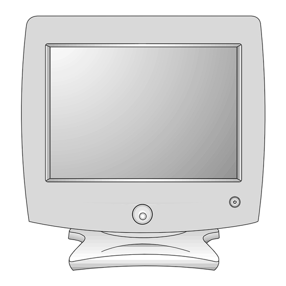
Page 1: Color Monitor
COLOR MONITOR SERVICE MANUAL CHASSIS NO. : CA-85 MODEL: CG572E, EV500 ID LABEL: EV500B CAUTION BEFORE SERVICING THE UNIT, READ THE SAFETY PRECAUTIONS IN THIS MANUAL. *NEW MODEL Issue Date: AUGUST 2000. -
Page 2: Table Of Contents
CONTENTS SPECIFICATIONS ........... 2 DESCRIPTION OF BLOCK DIAGRAM....12 SAFETY PRECAUTIONS ........3 ADJUSTMENT ............14 TIMING CHART ............4 TROUBLESHOOTING GUIDE ......16 OPERATING INSTRUCTIONS ........ 5 EXPLODED VIEW........... 26 CONTROL LOCATIONS ......... 7 REPLACEMENT PARTS LIST ....... 28 WIRING DIAGRAM .......... -
Page 3: Safety Precautions
24.5kV. The following steps describe modify the original design without obtaining written how to measure the high voltage and how to prevent X- permission from GATEWAY or you will void the original radiation. parts and labor guarantee. -
Page 4: Timing Chart
TIMING CHART VIDEO SYNC FACTORY PRESET MODE MODE MODE 7 MARK MODE 1 MODE 2 MODE 3 MODE 4 MODE 5 MODE 6 MODE 8 — — — Sync Polarity — 60.023 Frequency 31.469 37.500 31.470 37.879 46.875 63.981 48.363 16.660 Total Period 31.778... -
Page 5: Operating Instructions
OPERATING INSTRUCTIONS FRONT VIEW REAR VIEW EV500 Gateway AC Power Socket Signal Cable Power ON/OFF Button Power (DPMS) Indicator Front Control Panel EV500 Gateway 3. OSD Select/Adjustment 2. Power (DPMS) Indicator 1. Power ON/OFF Button 1. Power ON/OFF Button 3. OSD Select/Adjustment This button is used to turn the monitor ON and OFF. - Page 6 On Screen Display (OSD) Control Icon Description To adjust an image size, position, and operating Mode Recall: To recall factory preset mode. parameters are quick and easy with the On Screen Display control system, using the OSD Select/Adjustment knob. A Advanced Option: There are five kinds of options.
-
Page 7: Control Locations
CONTROL LOCATIONS CONTROL MAIN Ref. No. Control Function Control Function Ref. No. SW201 POWER BUTTON OSD SELECT/ADJUSTMENT VR201 - 7 -... -
Page 8: Wiring Diagram
WIRING DIAGRAM P201 P501 P401 P702 P902 P402 Socket Signal Cable P301 P302 EARTH - 8 -... -
Page 9: Disassembly
DISASSEMBLY 2. BACK COVER REMOVAL 1. TILT/SWIVEL REMOVAL 1) Remove two screw caps (a). 1) Set the monitor face downward. 2) Remove four screws (b). 2) Pressing the latch (a), carefully remove 3) Slide the Back Cover away from the Front the Tilt/Swivel by pulling it upward. - Page 10 6. BOTTOM BRACKET REMOVAL 4. CONTROL PCB ASSEMBLY REMOVAL 1) Remove eight screws (a). 1) Remove three screws (a). 2) Remove the Bottom Bracket. 2) Remove the Control PCB Assembly from the Front Cabinet. 5. VIDEO PCB ASSEMBLY REMOVAL 1) Disconnect P301, P302, P1 from the Video PCB.
-
Page 11: Block Diagram
BLOCK DIAGRAM Focus Screen - 11 -... -
Page 12: Description Of Block Diagram
DESCRIPTION OF BLOCK DIAGRAM 1. Line Filter & Associated Circuit. 6. Horizontal and Vertical Oscillation. This is used for suppressing noise of power input line This circuit generates the horizontal pulse and the vertical flowing into the monitor and/or some noise generated in pulse by taking the H and V sync signal. - Page 13 15. Video Pre-Amp Circuit. 16. Video Output Amp Circuit. This circuit amplifies the analog video signal from 0-0.7V This circuit amplifies the video signal which comes from to 0-4V. It is operated by taking the clamp, R, G, B drive the video pre-amp circuit and amplified it to applied the and contrast signal from the Micom(IC401).
-
Page 14: Adjustment
1) Display cross hatch pattern at Mode 1~8. 10) PRESET EXIT → Y (Yes) command. 2) Run alignment program for CG572E on the 11) Display color 15,0 full Window pattern (70x70mm) at IBM compatible PC. Mode 3. - Page 15 17) PRESET EXIT → Y (Yes) command. 5. Adjustment for Focus. 18) Display color 15,0 full white patten at Mode 3. 1) Set the Brightness and Contrast to max position. 19) COLOR ADJ. → LUMINANCE → ABL command. 2) Display H character in full screen at Mode 7. 3) Adjust Focus control on the FBT that focus should ±...
-
Page 16: Troubleshooting Guide
TROUBLESHOOTING GUIDE 1. NO POWER NO POWER (POWER INDICATOR OFF) CHECK TROUBLE IN FUSE FUSE OK? (F901) CHECK C908 VOLTAGE? TROUBLE IN (AC120V: 160VDC, D901, D902, D903, D904 AC220V: 304VDC) CHECK IC901 PIN 6 TROUBLE IN WAVEFORM (SQUARE WAVE IC901 COMES OUT?) CHECK TROUBLE IN... - Page 17 2. NO CHARACTER NO CHARACTER CHECK TROUBLE IN IC302 P302 6.3V LINE PIN 17(6.3V) ? TROUBLE IN CHECK PC SIGNAL, IC302 PIN 1, 3, 5? P301 SIGNAL CABLE CHECK TROUBLE IN IC302 PIN 14, 16, 18 ? IC302 CHECK TROUBLE IN IC303 PIN 4 (105V) P302 15V LINE/ PIN 8 (15V) ?
- Page 18 3. NO RASTER NO VIDEO (POWER INDICATOR ON) CHECK AMBER DPM MODE POWER INDICATOR (NO H and/or V SYNC) GREEN or AMBER? GREEN CHECK TROUBLE IN D712 ANODE D712 (-120V)? CHECK TROUBLE IN G1 VOLTAGE? Q704 ( 35~-15V) CHECK TROUBLE IN CDT HEAT D941, Q942, Q941 VOLTAGE? (6.3V)
- Page 19 4. NO HORIZONTAL DEFLECTION NO H-DEFLECTION (ONE VERTICAL LINE) TROUBLE IN CHECK Q706? Q706 CHECK TROUBLE IN B + VOLTAGE 50V LINE (50V)? CHECK T701(FBT) PIN 2 TROUBLE IN (31KHZ 70V, Q719, Q720, Q717, D710 69KHZ 143V) ? CHECK TROUBLE IN Q705 COLLECTOR Q705 WAVEFORM?
- Page 20 5. TROUBLE IN H-LINEARITY UNBALANCED OF H-LIN. CHECK TROUBLE IN IC401 IC401 (MICOM) PIN 22, 23, 24 ? CHECK TROUBLE IN Q711~Q716? Q711 ~ Q716 CHECK TROUBLE IN L703? L703 Cs SIGNAL TABLE HORIZONTAK FREQUENCY(fH) TROUBLE IN 29K ~ 35.9K C722, C723, C726, C729 36K ~ 38.9K 39K ~ 48.9K...
-
Page 21: No Vertical Deflection
6. NO VERTICAL DEFLECTION NO V-DEFLECTION (ONE HORIZONTAL LINE) CHECK TROUBLE IN IC601 PIN 3 D602 15V LINE (15V)? TROUBLE IN CHECK -12V LINE IC601 PIN 4 D953, C605, C606, C962 (-12V)? CHECK TROUBLE IN IC701 PIN 23? IC701 TROUBLE IN IC601, V-CIRCUIT - 21 -... - Page 22 7. TROUBLE IN OSD (ENTER BUTTON MUST BE PRESSED.) NO OSD CHECK TROUBLE IN IC301 B + ? 5V LINE DC 5V CHECK TROUBLE IN IC301 PIN 5, 10 IC601 PIN8 (V-FBP), WAVEFORM? T701 40V LINE (H-FBP) negative pulse Pin 10 negative pulse Pin 5 CHECK...
- Page 23 8. TROUBLE IN DPM (NO OFF MODE.) OFF MODE FAILURE CHECK CHECK PC, IC401 (MICOM) INPUT H/V SYNC SIGNAL (PC IS NOT GOING INTO PIN 1, 42 (H/V INPUT) DPM OFF MODE) SIGNAL? H/V SYNC CHECK TROUBLE IN IC401 PIN 6 X401 WAVEFORM? 24MHz...
-
Page 24: No Degaussing
9. NO DEGAUSSING NO DEGAUSSING (DEGAUSS ON THE OSD MENU MUST BE PRESSED.) CHECK TROUBLE IN IC401 PIN 31 IC401 (MICOM) (0V)? CHECK TROUBLE IN Q953 COLLECTOR Q953 VOLTAGE? DC 15V CHECK TROUBLE IN P902 ? P902 CHECK TROUBLE IN RL901? RL901 TROUBLE IN... - Page 25 10. NO TILT (NO ROTATION ) NO TILT (NO ROTATION) CHECK TROUBLE IN Q504(COLLECTOR) IC401 ( MI COM) WAVE FORM ? CHECK TROUBLE IN 15V LINE 15V LINE, 6.3V LINE AND 6.3V LINE ? CHECK TROUBLE IN Q503 EMITTER Q501~Q503 VOLTAGE ? TROUBLE IN P501, TILT COIL, D501...
-
Page 26: Exploded View
EXPLODED VIEW EXPLODED VIEW PARTS LIST Ref. No. Part No. Description Q'ty Material *Remark 3091TKB033B CABINET ASS'Y, KCG572E G/WAY 028 2423GB0A81Z CDT, M36LBL803X00NLLW 339-002D SCREW ASS’Y, PHP+5x30BP+GW18 150-A29A COIL, DEGAUSSING 870MM 8.4 OHM 6174Z-1035A FBT, FMMTC81-M1035A 6620TKB002A SOCKET(CIRC), POWER BCP-03A 6871TST193B PWB(PCB), CG572C CONTROL REV1.0 4810TKK145A... -
Page 27: Replacement Parts List
REPLACEMENT PARTS LIST CAUTION: BEFORE REPLACING ANY OF THESE COMPONENTS, READ CAREFULLY THE SAFETY PRECAUTIONS IN THIS MANUAL. * NOTE SAFETY Mark AL ALTERNATIVE PARTS MODEL: EV500 DATE: 2000. 9. 16. LOC. NO. PART NO. DESCRIPTION / SPECIFICATION REMARK CAPACITORs C201 0CN1040K949 CAPACITOR, TUBULAR(HIGH DIELEC), 0.1M 50V Z F TA52... - Page 28 MODEL: EV500 DATE: 2000. 9. 16. LOC. NO. PART NO. DESCRIPTION / SPECIFICATION REMARK C609 181-288B CAPACITOR, POLYESTER, MKT 100V 104JTR PHS26104 C610 181-288Q CAPACITOR, POLYESTER, MKT 100V 154JTR PHS26154 C701 181-288B CAPACITOR, POLYESTER, MKT 100V 104JTR PHS26104 C702 181-288N CAPACITOR, POLYESTER, MKT 100V 103JTR PHS86103 C703 0CK8210K515...
- Page 29 MODEL: EV500 DATE: 2000. 9. 16. LOC. NO. PART NO. DESCRIPTION / SPECIFICATION REMARK C915 0CK1010K515 CAPACITOR, CERAMIC (HIGH DIELECTRIC), 100PF 50V K B TR C916 0CE106CK638 CAPACITOR, AL.ELECTROLYTIC, 10UF SHL,SD 50V M FM5 TP 5 C917 0CK1020K515 CAPACITOR, CERAMIC (HIGH DIELECTRIC), 1000PF 50V K B TR C918 0CK1040K945 CAPACITOR, CERAMIC (HIGH DIELECTRIC), 0.1UF 50V Z F TR...
- Page 30 MODEL: EV500 DATE: 2000. 9. 16. LOC. NO. PART NO. DESCRIPTION / SPECIFICATION REMARK D910 0DS113309AA DIODE, SWITCHING, 1SS133 TP ROHM KOREA DO34 90V 0.4A 0.6A D911 0DS113309AA DIODE, SWITCHING, 1SS133 TP ROHM KOREA DO34 90V 0.4A 0.6A D912 0DS113309AA DIODE, SWITCHING, 1SS133 TP ROHM KOREA DO34 90V 0.4A 0.6A D923 0DR153979BA...
- Page 31 MODEL: EV500 DATE: 2000. 9. 16. LOC. NO. PART NO. DESCRIPTION / SPECIFICATION REMARK FB904 125-155P CORE (CIRC), BEAD, BFS2550R2FG SAMWHA 2.5*5.0MM RADIAL FB905 125-155P CORE (CIRC), BEAD, BFS2550R2FG SAMWHA 2.5*5.0MM RADIAL FB906 125-159A CORE (CIRC), BEAD, FERRITE KQ-1 (RADIAL TAPPING) FB907 125-159A CORE (CIRC), BEAD, FERRITE KQ-1 (RADIAL TAPPING)
- Page 32 MODEL: EV500 DATE: 2000. 9. 16. LOC. NO. PART NO. DESCRIPTION / SPECIFICATION REMARK R215 0RD1001Q609 RESISTOR, FIXED CARBON FILM, 1K 1/4W(3 5% TA52 R217 0RD3600Q609 RESISTOR, FIXED CARBON FILM, 360 1/4W(3 5% TA52 R218 0RD3600Q609 RESISTOR, FIXED CARBON FILM, 360 1/4W(3 5% TA52 R219 0RD4300Q609 RESISTOR, FIXED CARBON FILM, 430 1/4W(3 5% TA52...
- Page 33 MODEL: EV500 DATE: 2000. 9. 16. LOC. NO. PART NO. DESCRIPTION / SPECIFICATION REMARK R503 0RD8201Q609 RESISTOR, FIXED CARBON FILM, 8.20K 1/4W(3 5% TA52 R504 0RD1500Q609 RESISTOR, FIXED CARBON FILM, 150 1/4W(3 5% TA52 R505 0RD2201Q609 RESISTOR, FIXED CARBON FILM, 2.20K 1/4W(3 5% TA52 R506 0RD1001Q609 RESISTOR, FIXED CARBON FILM, 1K 1/4W(3 5% TA52...
- Page 34 MODEL: EV500 DATE: 2000. 9. 16. LOC. NO. PART NO. DESCRIPTION / SPECIFICATION REMARK R761 0RD3001Q609 RESISTOR, FIXED CARBON FILM, 3K 1/4W(3 5% TA52 R762 0RD3001Q609 RESISTOR, FIXED CARBON FILM, 3K 1/4W(3 5% TA52 R763 0RD3001Q609 RESISTOR, FIXED CARBON FILM, 3K 1/4W(3 5% TA52 R766 0RD1001Q609 RESISTOR, FIXED CARBON FILM, 1K 1/4W(3 5% TA52...
- Page 35 MODEL: EV500 DATE: 2000. 9. 16. LOC. NO. PART NO. DESCRIPTION / SPECIFICATION REMARK R953 0RX4700J609 RESISTOR, SMALL FIX METAL FILM OXIDE, 470 OHM 1 W 5% TA52 R954 0RD4701Q609 RESISTOR, FIXED CARBON FILM, 4.70K 1/4W(3 5% TA52 R955 0RD4701Q609 RESISTOR, FIXED CARBON FILM, 4.70K 1/4W(3 5% TA52 R956 0RD4701Q609...
-
Page 36: Pin Configuration
PIN CONFIGURATION KA7805 (KA7808, KA7812) Positive Voltage Regulator 5V (8V, 12V) BLOCK DIAGRAM SERIES INPUT OUTPUT PASS ELEMENT CURRENT GENERATOR PROTECTION STARTING REFERENCE ERROR CIRCUIT VOLTAGE AMPLIFIER 1: Input THERMAL 2: GND PROTECTION 3: Output TDA8172 Vertical Deflection Output Circuit NON-INVERTING INPUT OUTPUT STAGE SUPPLY OUYPUT... - Page 37 LSC4543 CMOS Graphic Monitor On-Screen Display SS(A) VCO(PCI) RP(NC) DD(A) HFLB(NC) FBKG VSYNC (MOSI) (SCK) Pin Configuration BLOCK DIAGRAM HORD VERO DISPLAY MEMORY OSD_EN SHADOW BSEN CONTROL X32B REGISTERS VPOL HPOL SDA(M0SI) and DATA DATA WADDR SCL(SCK) MANAGEMENT DATA RECEIVER MBUS/SPI WCOLOR CONTROL...
- Page 38 M24C08 8K SERIAL I C BUS EEPROM PIN NAME FUNCTION E0-E2 Chip Enable Inputs Serial Data Address Input/Output Serial Clock Write Control Supply Voltage M2404C08 Ground Pin Configuration - 39 -...
- Page 39 TYPE PARTS TYPE PARTS 2N3904 KTA1275 KTD1413 IRFS630A KTC200-Y KIA7042 KTC3198 KSB564AC DTC114E - 40 -...
- Page 40 3.40V 85.2V 0V(Grand) - 45V - 5V - 0V - 7V 50.4V 15.6V 1.88V...
-
Page 41: Printed Circuit Board
PRINTED CIRCUIT BOARD 1. MAIN BOARD (Component Side) 2. MAIN BOARD (Solder Side) 3. VIDEO BOARD (Component Side) 4. VIDEO BOARD (Solder Side) 5. CONTROL BOARD (Component Side) 6. CONTROL BOARD (Solder Side) - Page 42 PACKING AND ACCESSORIES Owner’s Manual Power Cord Top Packing Signal Cable Bottom Packing - 45 -...
- Page 43 Jul. 2000 P/NO : 3828TSO038A Printed in Korea...
Need help?
Do you have a question about the CG572E and is the answer not in the manual?
Questions and answers