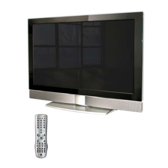
Vizio GV46L HDTV Service Manual
For samsung panel
Hide thumbs
Also See for GV46L HDTV:
- User manual (80 pages) ,
- Quick start manual (2 pages) ,
- User manual (79 pages)

Related Manuals for Vizio GV46L HDTV


Summary of Contents for Vizio GV46L HDTV
- Page 1 Service Manual Model #: VIZIO GV46L HDTV VIZIO GV46L HDTV10A (For Samsung Panel) V, Inc 320A Kalmus Drive Costa Mesa, CA 92626 TEL : +714-668-0588 FAX :+714-668-9099 Top Confidential...
-
Page 2: Table Of Contents
11. Spare parts list 11-1 12-1. Complete Parts List (GV46L HDTV_Samsung) 12-1 12-2. Complete Parts List (GV46L HDTV10A_Samsung) 12-2 Appendix 1. Main Board Circuit Diagram 2. Main Board PCB Layout 3. Assembly Explosion Drawing Block Diagram VIZIO GV46L_HDTV,GV46L_HDTV10A Service Manual... - Page 3 Use a power cable that is properly grounded. Always use the AC cords as follows – USA (UL); Canada (CSA); Germany (VDE); Switzerland (SEV); Britain (BASEC/BS); Japan (Electric Appliance Control Act); or an AC cord that meets the local safety standards. VIZIO GV46L_HDTV,GV46L_HDTV10A Service Manual...
-
Page 4: Chapter 1 Features
Chapter 1 Features High resolution 1366 x 768 with wide screen Built-in digital HDTV and standard TV combination TV tuner All TV formats supported (1080i, 720p, 480 p and 480i) Computer Monitor (RGB): up to1366 x 768 (H x V) Wall mounting capable with and without speakers 2.1 virtual surround sound (TruSurround XT) with 20W subwoofer Dual HDMI (High Definition Multimedia Interface) -
Page 5: Specifications
Chapter 2 Specification 1. General specification Native Resolution 1366 (H)X768 (V) pixels, Effective Display Size 1018.353 (H) x 572.544 (V) mm Aspect Ratio 16:9 Display Color 8 bit, 16.7M Brightness 400 cd/ m (Min) 1,200:1 (Typical, panel spec). Contrast Ratio NTSC/ATSC/ QAM TV system 15pins D-sub, HDMI-DVI... -
Page 6: Optical Characteristics
2. Optical characteristics Item Specification Note Display Pixels 1366 (H) x 768 (V) pixels Pixel Pitch 0.7455 (H) x0.2485 (V) mm*3 Pixel Arrangement RGB vertical stripe Color Depth 8 bit, 16.7M colors Active Display Area 921.6 (H) x 519.2 (V) ±0.5 mm Surface treatment of Hard coating Brightness... - Page 7 4. Environment 4.1 Operating a. Temperature 0~35 b. Humidity 0%~90% RH (No condensation) 4.2 Non-operating a. Temperature -20~60 b. Humidity 0%~90% RH (No condensation) 4.3 Altitude a. Operating 0~14,000 ft b. Non-operating 0~40,000 ft 5. Dimensions & Weight A: Display Module B: Speaker C: Base Display Module +...
- Page 8 6. Packaging Specification 6.1 Packaged dimensions a. Height 960+/- 20 mm b. Width 1300+/- 20mm c. Depth 374 +/- 20 mm 6.2 Pallet Load a. Sea 3 units/pallet 6.3 Container Load a. 40’ container 108 units (@3 x 36 pallets= 108 units) b.
-
Page 9: On Screen Display
Chapter 3 On Screen Display 1. Analog Menu - RGB/AV/Component/HDMI/TV Image Settings Mode Level 1 Level 2 Level 3 Level 4 Vivid, Movie, Game, VIDEO Picture Mode Sport, Custom VIDEO Brightness(0~100) VIDEO Contrast(O~100) VIDEO Saturation(0 100) VIDEO Hue(-50~50) VIDEO Sharpness(0~24) VIDEO Advanced VIDEO Noise Reduction... - Page 10 When “Custom” in “Picture Mode” is selected. Display Settings Mode Level 1 Level 2 Level 3 Level 4 16:9 4:3 Zoom* VIDEO Aspect Ratio Panoramic** 16:9 4:3 Aspect Ratio PIP Mode Off, Large PIP, Small PIP, POP PIP Position Top-Left, Top-Right, Bottom-Left, Bottom-Right PIP Input ***...
- Page 11 Parental Controls Mode Level 1 Level 2 Level 3 Level 4 VIDEO Password VIDEO Settings VIDEO TV Rating TV Youth (Unblocked Blocked) VIDEO TV Youth 7 (Unblocked Blocked) VIDEO VIDEO TV G (Unblocked Blocked) TV PG (Unblocked Blocked) VIDEO TV 14 (Unblocked Blocked) VIDEO TV MA (Unblocked Blocked) VIDEO...
- Page 12 Setup Mode Level 1 Level 2 Level 3 Level 4 Closed Caption Display CC1, CC2, CC3, CC4, TEXT1, TEXT2, TEXT3, TEXT4 Captions on mute On, Off Language English, French, Spanish Factory Reset (No,Yes) Image Cleaner TV Menu Auto Scan Set Channel Add/Skip Cable/Antenna DTV Menu*...
- Page 13 Level 1 Level 2 Level 3 Level 4 Level 5 Scan* Manual Scan* Scan mode Add-on Mode Range Mode From Channel To Channel Channel Skip Digital Audio Out Dolby Digital Closed Caption Analog Closed CC1~CC4 OFF Caption Digital Closed Service 1~Service 6, CAPTION Digital Closed Style As Broadcaster...
- Page 14 Level 1 Level 2 Level 3 Level 4 Level 5 Background Color Black White Green Blue Cyan Yellow Magenta Background Opacity Solid Translucent Transparent Window Color Black White Green Blue Cyan Yellow Magenta Window Opacity Solid Translucent Transparent Parental control CONFIDENTIAL –...
-
Page 15: Factory Preset Timings
Chapter 4 Factory preset timings This timing chart is already preset for this LCD TV. 1. RGB PC preset modes Horizontal Vertical Refresh Horizontal Vertical Mode Sync Sync Pixel Rate Resolution Rate Frequency Frequency Remark Polarity Polarity (MHz) (Hz) (KHz) (Hz) (TTL) (TTL) - Page 16 3. HDMI- DVI preset modes - through HDMI interface by an optional interface cable 3.1 Video input Mode No. Resolution 480i 480p 720p 1080i 3.2 PC input Horizontal Vertical Refresh Horizontal Vertical Mode Sync Sync Pixel Rate Resolution Rate Frequency Frequency Remark Polarity...
-
Page 17: Pin Assignment
Chapter 5 Pin Assignment 1. Input RGB PC Connector a. Type: Analog b. Frequency: H: 30-80KHz V: 60-85Hz c. Signal level: 0.7Vp-p d. Impedance: e. Synchronization H/V separate sync: H/V composite sync: Sync on Green f. Video bandwidth: 135MHz g. Connector type: 15-pin D-Sub, female Pin Number Pin Assignment... - Page 18 HDMI Connector a. Frequency: H: 15.734KHz V: 60Hz H: 31KHz V: 60Hz H: 45KHz V: 60Hz H: 33KHz V: 60Hz b. Polarity: Positive or Negative c. Type: Type A d. Pin Assignment: Please see below Pin 19 Pin 1 Pin 2 Signal Assignment Signal Assignment TMDS Data2+...
- Page 19 1.3 AV/Composite Video (CVBS) Connector a. Frequency: H: 15.734KHz V: 60Hz (NTSC) b. Signal level: 1Vp-p Sync (H+V):0.3V below Video (Y+C) c. Impedance: d. Connector type: RCA jack 1.4 AV/S-Video Connector 1, 2 = GND 3 = Luminance (Y) 4 = Chrominance(C) a.
- Page 20 F-type TV RF connector NTSC system a. Signal level Analog 1Vp-p typical (45tdB~90dB) b. Frequency 55~801 MHz ATSC system a. IF-output level 1Vp-p minimum b. Frequency 57~803 MHz QAM system (supporting clear QAM) a. IF-output level 1Vp-p minimum b. Frequency 57~849 MHz PC Stereo audio a.
- Page 21 2.3 Headphone a. Signal level: 1Vrms (max.) b. Impedance: c. Output: 50 mW d. Connector type: Earphone mini jack 3. Acoustic 3.1 Connection 3.1.1 Left Acoustic: Speaker connector (5-pin audio din) connected to the speaker box with 2” x 5” 8 /10 W speaker 3.1.2 Right Acoustic: Speaker connector (5-pin audio din) connected to the speaker box with 2”...
-
Page 22: Block Diagram
Chapter 6 Block Diagram System Block Diagram LVDS BOARD INVERTER BOARD INVERTER BOARD POWER BOARD AUDIO BOARD MAIN BOARD IR BOARD CORE CONFIDENTIAL – DO NOT COPY Page 6-1 File No. SG-0199... - Page 23 Main board System Block Diagram ARXD VEDIO ATXD U60 TS5V330 ATXD_HUD ARXD_HUD U40 24LC128 EEPROM(8051) HY5DU56822CT-D4 HY5DU56822CT-D4 U20 4052 51_RXD/51_TXD U17 DDR RAM CTZ U16 DDR RAM HUD I/O SW UC_SCL/UC_SDA LED BLACKLIGHT SST89C58 FL8532_CTZ Frame Store Frame Store DDR Interface DDR Interface KEY PAD + IR ADATA[0:23]...
- Page 24 Chapter 7 Main/ATSC Board Internal I/O Connections MAIN Board CN1 “DC POWER INPUT’ Description PDP_+5Vsc PDP_+5Vsc PDP_+5Vsc PDP_+12V PDP_+12V PDP_+12V_FAN PDP_FGND CN2 “DC POWER INPUT’ Description PDP_Audio PDP_Audio CN3 “DC POWER INPUT/OUTPUT’ Description VS_ON RLY_ON PDP_+5Vsb BRIGHT CONFIDENTIAL – DO NOT COPY Page 7-1 File No.
- Page 25 CN5 CONNECTION “KEYPAD” Description LED2_KEYPAD KEY_VCC ADC_IN2 +3.3V_LBADC ADC_IN1 LED1_KEYPAD_BUF CN6 CONNECTION “HDMI/ATSC_UP” Description 51_TXD 51_RXD CN7 CONNECTTION “ODC2BI” Description VGA_SCL_CTZ VGA_SDA_CTZ CONFIDENTIAL – DO NOT COPY Page 7-2 File No. SG-0199...
- Page 26 CN12 FAN CONNECTION Description FANIN1 +12V_FAN FGND CN13 FAN CONNECTION Description FANIN1 +12V_FAN FGND J11 CONNECTION “AUDIO BOARD” Description AUDIO_EXT_R AUDIO_EXT_L MUTE_AMP AUDIO_SUB CONFIDENTIAL – DO NOT COPY Page 7-3 File No. SG-0199...
- Page 27 W1 CONNECTION “LVDS” Description Description TXA3+ TXA3- TXAC+ TXAC- TXA2+ TXA2- TXA1+ TXA1- TXA0+ TXA0- +5V_SW +5V_SW +5V_SW TXB3+ TXB3- VS_ON SCL_33V SDA_33V CONFIDENTIAL – DO NOT COPY Page 7-4 File No. SG-0199...
- Page 28 W1 CONNECTION “ATSC BOARD” Description Description SCL_5V ATSC_CLK SDA_5V ATSC_RST ATSC_WS ATSC_RDY ATSC_DA SV1_CTZ / SV1_HUD ATSC_Y N / C ATSC_Pb SIF_Tuner1 ATSC_Pr SIF_Tuner2 N / C N / C +12V_SW ATSC_Audio_L +12V_SW ATSC_Audio_R +5V_SW ATSC_TX +5V_SW ATSC_RX +5V_SW CHKTNR0 +5V_SW +5V_SW J3 SELECT KEY POWER...
- Page 29 ATSC Board W1 CONNECTION “MAIN BOARD” Description Description Tuner-SCL2 A01MICLK/A01BLK Tuner-SDA2 ORESET A01LRCK READY A01SDATA0 NTSC-CVB1 MAIN-YOUT N / C MAIN-PbOUT NTSC-SIF MAIN_PrOUT N / C HDMI-SPDIF SPDIF-Ctrl +12V_SW Audio_LCHOUT +12V_SW Audio_RCHOUT N / C U2TX N / C U2RX N / C Tuner SW N / C...
- Page 30 AUDIO Board J1 CONNECTION “MAIN BOARD” Description AUDIO_EXT_R AUDIO_EXT_L MUTE_AMP AUDIO_SUB J4 CONNECTION “POWER BOARD” Description J3 CONNECTION “SPEAKER L” Description LOUT CONFIDENTIAL – DO NOT COPY Page 7-7 File No. SG-0199...
- Page 31 J1 CONNECTION “SPEAKER R” Description ROUT SWOUT SWOUT SWOUT SWOUT CONFIDENTIAL – DO NOT COPY Page 7-8 File No. SG-0199...
-
Page 32: Theory Of Circuit Operation
Chapter 8 Theory of Circuit Operation The operation of User Interface The following diagram provides a brief overview of the user-interactive components of the firmware. Figure 8-1 User Interface Block Diagram The operation of keypad There are 7 keys to control and select the function of SHD-3010 and also have two LED to indicate the status of operation. -
Page 33: Features
The operation of Video Processor FLI8532 The Genesis Microchip FLI8532 includes an integrated 3-D Digital Video Decoder with Faroudja DCDi CinemaTM video format conversion, video enhancement, and noise reduction. The auto-detection and Faroudja DCDi CinemaTM technology allow the FLI8532 to detect, process, and enhance any video or PC graphic format. - Page 34 Analog Input Port (AFE): The FLI8532 chip has a sophisticated Analog Front End with 16 reconfigurable inputs through and analog multiplexer to anti-alias filters before the Analog to Digital Converters (ADCs). These integrated features eliminate the need for any devices between the input connector and the pin of the FLI8532.
- Page 35 PORTA also includes optional signals (DIP_EXT_CLAMP, DIP_EXT_COAST, DIP_CLEAN_HS_OUT) for interfacing to external ADC/PLL devices. These signals are not present on PORTB. Bits 7 to 0 of PORTA can be configured as a bidirectional interface for media card applications. Inputs to the digital input port are TTL compatible with a maximum clock speed of 135MHz.
- Page 36 LVDS Transmitter: Two LVDS channels (A and B) are available on the output of the FLI8532 to transmit data and timing information to the display device. The following diagram shows the available LVDS mapping for 30-bit LVDS output which is applying to PDP panel spec: 30-bit LVDS Output Stream To Configure for 30-bit LVDS with this data mapping:...
- Page 37 On Chip Microcontroller: FLI8532 on-chip micro-controller (OCM) serves as the system micro-controller. It programs the FLI8532 and manages other devices in the system such as the keypad and non-volatile RAM (NVRAM) using general-purpose input/output (GPIO) pins. The OCM can address a 22-bit address space to utilize 4 MB external ROM Figure 8-5 FLI8532 OCM block diagram The OCM executes a firmware program running from external ROM, as well as driver-level (or Application Programming Interface –...
- Page 38 The two-wire protocol requires each slave device to be addressable by a 7-bit identification number. A two-wire data transfer consists of a stream of serially transmitted bytes formatted as shown in the figure below. A transfer is initiated (START) by a high-to-low transition on MSTR_SDA while MSTR_SCL is held high.
- Page 39 Clock Generation The FLI8125 accepts the following input sources: 1.Crystal Input Clock (TCLK and XTAL). This is the input pair to an internal crystal oscillator and corresponding logic. Alternatively, a single ended TTL/CMOS clock input can be driven into the XTAL pin (leave TCLK as n/c in this case). 2.External Clocks on various GPIOs for test purposes 3.Host Interface Transfer Clock (SCL), I2C slave SCL for DDC2Bi and another SCL for Serial Inter-Processor Communication (SIPC)
- Page 40 Figure 8-8 FLI8125 Internally Synthesized Clocks Analog Front End The Analog Front End is responsible for selecting and capturing the desired analog input video stream. Overall application cost is reduced by providing analog switching capabilities for 16 separate analog signals. These signals are re-configurable as different combinations of composite, S-Video, YPrPb and RGB video streams depending upon the end application.
- Page 41 Figure 8-9 Analog Input Port The Analog Front End provides the capability to capture 16 analog video inputs which can be a combination of Composite (CVBS), S-Video (SY, SC), YPrPb (Y, Pr, Pb) or RGB (R, G, B). The Analog Source Selectors are responsible for switching the desired analog inputs to the ADCs for digitization.
- Page 42 Figure 8-10 Digital Datapath Digital Input Port The Digital Input Port is 24-bit input bus that can be connected to external DVI receivers, video decoders, etc. and is able to accept either 8-bit CCIR656 data, 16-bit 4:2:2 YUV data or 24-bit RGB data.
- Page 43 Input Capture The Input Capture block is responsible for extracting valid data from the input data stream and creating the required synchronization signals required by the data pipeline. This block also provides stable timing when no stable input timing exists. The selected input data stream is cropped using a programmable input capture window.
- Page 44 Image Processing The following figure shows the various image processing blocks that operate on the captured video data stream. Each block is individually selectable and can be removed from the processing chain via a selectable bypass path. When a processing block is bypassed, it automatically enters a low power mode to help reduce overall power consumption.
- Page 45 Display Output Interface The Display Output Port provides data and control signals that permit the connection to a variety of flat panel devices using a 24-bit TTL or LVDS interface. The output interface is configurable for single or dual wide LVDS in 18 or 24-bit RGB pixels format. All display data and timing signals are synchronous with the DCLK display clock.
- Page 46 Figure 8-13 Display Windows and Timing Data captured by the Input Capture Window and processed by the various image manipulation blocks is output in the Display Active Window. This window is always in the foreground and lies on top of all other output windows, except OSD overlay windows. Typically the Display Active Window is set to the same size as the output of the Scaling Engine.
- Page 47 The benefit of dithering is that the eye tends to average neighboring pixels and a smooth image free of contours is perceived. Dithering works by spreading the quantization error over neighboring pixels both spatially and temporally. Two dithering algorithms are available: random or ordered dithering.
- Page 48 Figure 8-14 FLI8125 OCM Programming The operation of HDMI Sil9011 The SiI 9011 provides one HDMI input port. The SiI 9011 video output goes to a video processor while the audio output goes to an audio DAC. CONFIDENTIAL – DO NOT COPY Page 8-17 File No.
- Page 49 Figure 8-15 HDMI 9011 Block Diagram TMDS Digital Core The core performs 10-to-8-bit TMDS decoding on the audio and video data received from the three TMDS differential data lines along with a TMDS differential clock. The TMDS core supports link clock rates to 165MHz, including CE modes to 720p/1080i/1080p and PC modes to XGA, SXGA and UXGA.
- Page 50 Data Input and Conversion Mode Control Logic The mode control logic determines if the decrypted data is video, audio or auxiliary information, and directs it to the appropriate logic block. Video Data Conversion and Video Output The SiI 9011 can output video in many different formats (see examples in Table 2). The receiver can also process the video data before it is output, as shown in Figure 5.
- Page 51 The operation of TV route TV signal is processes to the tuner and output toMTK8205 the MTK8205 generates the vertical and horizontal timing signals for display device. Audio is processes to the tuner output to SIF circuit and output to 4450. The operation of DTV route DTV signal is processes to the tuner and output to MT5112 who handle ATSC input to match MPEG-2 package, then transfer to MT5351.
-
Page 52: Waveforms
Chapter 9 Waveforms 1. Ripple Voltage (1) PDP_+5Vsc (CN1.1) (2) PDP_+12V (CN1.7) CONFIDENTIAL – DO NOT COPY Page 9-1 File No. SG-0199... - Page 53 (3) PDP_+5Vsb (CN3.4) (4) FLI8125 (U10) +3.3V_I/O_HUD CONFIDENTIAL – DO NOT COPY Page 9-2 File No. SG-0199...
- Page 54 +3.3V_ADC_HUD +1.8V_ADC_HUD CONFIDENTIAL – DO NOT COPY Page 9-3 File No. SG-0199...
- Page 55 (5) FLI8532 (U13) +3.3V_I/O +1.8V_ADC CONFIDENTIAL – DO NOT COPY Page 9-4 File No. SG-0199...
- Page 56 +2.5V_DDR +1.8V_CORE CONFIDENTIAL – DO NOT COPY Page 9-5 File No. SG-0199...
- Page 57 (6) NT5DS16M16CS-5T (U16, U17) (7) Am29LV320DT90-ED (XU1) CONFIDENTIAL – DO NOT COPY Page 9-6 File No. SG-0199...
- Page 58 (8) LM2660 (-5V_N of the U29) CONFIDENTIAL – DO NOT COPY Page 9-7 File No. SG-0199...
- Page 59 2. Clock Timing (1) NT5DS16M16CS-5T DDR clock (pin 45 of the U16 or U17) (2) FLI8125 Crystal clock (pin 15 of the U10) CONFIDENTIAL – DO NOT COPY Page 9-8 File No. SG-0199...
- Page 60 Hudson output clock (3) FLI8532 Crystal clock (pin B26 of the U13 or pin 1 of the C155) Cortze output clock CONFIDENTIAL – DO NOT COPY Page 9-9 File No. SG-0199...
- Page 61 (4) MSP4450G crystal clock (pin 55 of the U32) CONFIDENTIAL – DO NOT COPY Page 9-10 File No. SG-0199...
- Page 62 (5) SiI9011CLU crystal clock (pin 84 of the U35 and U42) (6) IC SM5964C40J crystal clock (pin 20 of the U38) CONFIDENTIAL – DO NOT COPY Page 9-11 File No. SG-0199...
- Page 63 3. Horizontal and Vertical sync. Timing (1) VGA input (1024x768x60Hz) H-sync CONFIDENTIAL – DO NOT COPY Page 9-12 File No. SG-0199...
- Page 64 V-sync CONFIDENTIAL – DO NOT COPY Page 9-13 File No. SG-0199...
- Page 65 (2) SiI9011CLU (U35 and U42) BHS-sync CONFIDENTIAL – DO NOT COPY Page 9-14 File No. SG-0199...
- Page 66 BVS-sync CONFIDENTIAL – DO NOT COPY Page 9-15 File No. SG-0199...
- Page 67 CONFIDENTIAL – DO NOT COPY Page 9-16 File No. SG-0199...
- Page 68 ATSC Board 1. Voltage Measurement (1) 12V (+12V, C4) (2) 5V (+5V, C239) CONFIDENTIAL – DO NOT COPY Page 9-17 File No. SG-0199...
- Page 69 (3) 3.3V (DV33, C11) (4) 2.5V (DV25, C185) CONFIDENTIAL – DO NOT COPY Page 9-18 File No. SG-0199...
- Page 70 (5) 1.8V (DV18, C64) (6) 1.25V (+1V25_DDR, C148) CONFIDENTIAL – DO NOT COPY Page 9-19 File No. SG-0199...
- Page 71 (7) 1.2V (DV12, C26) CONFIDENTIAL – DO NOT COPY Page 9-20 File No. SG-0199...
- Page 72 2. Clock Timing (1) MT5351 Clock Timing (U10 B2-OXTALI) (2) MT5112 Clock Timing (U9 97-XTAL1 / 96-XTAL2) Ch1 – XTAL1 / Ch2 – XTAL2 CONFIDENTIAL – DO NOT COPY Page 9-21 File No. SG-0199...
- Page 73 (3) Memory Clock Timing (U13-45, MEM_CLKA) (4) Memory Clock Timing (U12-45, MEM_CLKA) CONFIDENTIAL – DO NOT COPY Page 9-22 File No. SG-0199...
-
Page 74: Trouble Shooting
Chapter 10 Trouble Shooting A. SYSTEM OVERVIEW Iverter board Power supply board AUDIO board Iverter board Main board Display board IR board ATSC Board CONFIDENTIAL – DO NOT COPY Page10-1 File No. SG-0199... - Page 75 B. PCB PARTS NAME/NUMBER AND FUNCTION DESCRIPTION PART NAME PART NUMBER FUNCTION ESCRIPTION POWER SUPPLY BOARD PROVIDE ALL THE POWER FOR TV SET 364600120150 AIN BOARD CONNECTING TO TRANSFER DISPLY SIGNAL AMPLIFIER THE AUDIO SIGNAL TO THE SPEAKER 364600120189 IR BOARD RECEIVE THE REMOTE CONTROLER AND DISPLAY SYSTEM STATUS LED 364600120156...
- Page 76 ISPLAY BOARD IR BOARD CONFIDENTIAL – DO NOT COPY Page10-3 File No. SG-0199...
- Page 77 ATSC BOARD AUDIO BOARD CONFIDENTIAL – DO NOT COPY Page10-4 File No. SG-0199...
- Page 78 PDP DISPLAY NOTHING 1. Main board & ATSC board block diagram ARXD VEDIO ATXD U60 TS5V330 ATXD_HUD ARXD_HUD U40 24LC128 EEPROM(8051) HY5DU56822CT-D4 HY5DU56822CT-D4 U20 4052 51_RXD/51_TXD U17 DDR RAM CTZ U16 DDR RAM HUD I/O SW UC_SCL/UC_SDA LED BLACKLIGHT SST89C58 FL8532_CTZ Frame Store Frame Store...
- Page 79 PDP DISPLAY NOTHING(Analog HD1/AC on/off default) Start Power LED is lighting? Check AC power cord Power LED is lighting? Press Meun or Info. Check input source Is there any OSD’s logo Remove R87. Check internal cable? Check W1 pin 27 is high? Check U13 pin AD14.
- Page 80 PDP DISPLAY NOTHING(Analog HD1 without Pb signal) BLOCK 1 Check component 1 Trace componect 1 from Is picture on screen? (Pb signal) C259 Input To U13 circuit Is there sync? Check R196,R198 Use GProbe connect from main to PC. U13 fail Does scaler detect the signal? PDP DISPLAY NOTHING(Analog HD1 without Pr signal) BLOCK 1...
- Page 81 PDP DISPLAY NOTHING(Analog HD1 on PIP mode without Pb signal) BLOCK 1 Check component 1 Trace componect 1 from Is picture on screen? (Pb signal) C255 Input To U10 circuit Is there sync? Check R200,R198 Use GProbe connect from main to PC. U10 fail Does scaler detect the signal? PDP DISPLAY NOTHING(Analog HD1 on PIP mode without Pr signal)
- Page 82 PDP DISPLAY NOTHING(Analog HD2 without Pb signal) BLOCK 1 Check U23 outnput pin 28 Check component 2 Input pin 15 Is no blue color on screen? (Pb signal) C260,R197 U23 fail Input clamp voltage pin 5(+5V) Is there sync? Output clamp voltage pin 29(+5V) VCC3 pin 22,23(+5V) Input_switch_select high(+5V) Use GProbe connect...
- Page 83 PDP DISPLAY NOTHING(Analog HD2 on PIP mode without Pb signal) BLOCK 1 Check U24 outnput pin 28 Check component 2 Input pin 15 Is no blue color on screen? (Pb signal) C288,R213 U24 fail Input clamp voltage pin 5(+5V) Is there sync? Output clamp voltage pin 29(+5V) VCC3 pin 22,23(+5V) Input_switch_select high(+5V)
- Page 84 PDP DISPLAY NOTHING(RGB on PIP mode without screen) BLOCK 1 Check U45 Check U45 H sync output U45 pin4,R181 Check U45 H sync input U45 pin1,R185 V sync output U45 pin8,R184 pin 14 +3.3V V sync input U45 pin5,R187 Is picture on screen? Is there signal? U45 fail Check input source...
- Page 85 PDP DISPLAY NOTHING(Composite 1 without screen) BLOCK 1 Check Q28’s Base. Check C310,R275,R274 Check Q28’s emitter. Is there signal? Q28 fail Is picture on screen? Is there signal? Is there signal? Check collector voltage(+5V). Use GProbe connect from main to PC. Q13 fail Does scaler detect the signal? Check:...
- Page 86 PDP DISPLAY NOTHING(Composite 2 without screen) BLOCK 1 Check Q29’s Base. Check C316,R286,R285 Check Q29’s emitter. Is there signal? Q29 fail Is picture on screen? Is there signal? Is there signal? Check collector voltage(+5V). Use GProbe connect from main to PC. Q13 fail Does scaler detect the signal? Check:...
- Page 87 PDP DISPLAY NOTHING(S-VIDEO 1 without screen) BLOCK 1 Check Q30’s Base. Check C320,R293,R292 Check Q30’s emitter. Is there signal? Is picture on screen? Q30 fail Is there signal? Is there signal? Check collector voltage(+5V). Use GProbe connect from main to PC. Q13 fail Does scaler detect the signal? Check:...
- Page 88 PDP DISPLAY NOTHING(S-VIDEO 1 on PIP mode without screen) BLOCK 1 Check Q30’s Base. Check C318,R291,R292 Check Q30’s emitter. Is there signal? Is picture on screen? Q30 fail Is there signal? Is there signal? Check collector voltage(+5V). Use GProbe connect from main to PC.
- Page 89 PDP DISPLAY NOTHING(S-VIDEO 2 without screen) BLOCK 1 Check Q33’s Base. Check C332,R316,R320 Check Q33’s emitter. Is there signal? Is picture on screen? Q33 fail Is there signal? Is there signal? Check collector voltage(+5V). Use GProbe connect from main to PC. U13 fail Does scaler detect the signal? Check:...
- Page 90 PDP DISPLAY NOTHING(S-VIDEO 2 on PIP mode without screen) BLOCK 1 Check Q33’s Base. Check C331,R313,R320 Check Q33’s emitter. Is there signal? Q33 fail Is picture on screen? Is there signal? Is there signal? Check collector voltage(+5V). Use GProbe connect from main to PC.
- Page 91 PDP DISPLAY NOTHING(Digital 2 U35 with PORT B without screen) BLOCK 1 Check input source? Is picture on screen? Check U37 I2C bus D66 fail Check U37 power Check D66 and D65 SCL Pin 6 5V Pin 8 Are there 5V output? SDA pin 5 D65 fail Check U35 pin 90...
- Page 92 Block 2 start HDMI’s chip Check U38’s power Check U2’s +5V_SW communicate with Pin 44,35 pin 7,8 SM5964,is ok? Check Y3 11.0592MHz Check U38’s UART Check U20 TxD pin 13 pin 16 +5V U20 fail RxD pin 11 Pin 10 output select=high Check R143,R144 U13 fail CONFIDENTIAL –...
- Page 93 DDC R ROUBLE OF EADING Start Support DDC2B 1.Analog cable ok? Analog DDC OK? 2.Voltage of +5V_BUF ok? 3.Check U21 4.Is compliant protocol? Support DDC2B 1.HDMI cable ok? Digital HDMI1 DDC OK? 2.Voltage of VCC5_E2P_2ok? 3.Check U44 4.Is compliant protocol? Support DDC2B 1.HDMI cable ok? Digital HDMI2 DDC OK?
- Page 94 PDP N O SOUND PDP NO SOUND Start Audio power DC power ok? Check F2 output has +24V? Audio power fail Check U19.8 and U19.9 Check audio AMP U19 has output? J11 Pin 1&3 Check C436,C430 input siganl? J11 Pin 1&3 Check Audio AMP U19 Audio board fail Block 3...
- Page 95 TROUBLE OF THE DTV CONFIDENTIAL – DO NOT COPY Page10-22 File No. SG-0199...
-
Page 96: Spare Parts List
Chapter 11 Spare Parts List PART NO DESCRIPTION REMARK 0185-1152-0073 FUSE 125V/1.5A SMD (R45101.5) L-F 0185-1502-0073 FUSE 125V/5A SMD (R45105) L-F 0280-2500-0012 X'TAL 25MHZ 49/US 30PPM 20PF LF 0286-2700-0024 OSC 27MHz 25ppm 3.3V SMD VCXO 0320-4000-0142 POWER CORD 110V UL/CSA 1800mm BLK N.M. (VINC) 0321-0000-0411 AV CABLE RCA(Y/W/R) 1800mm BLK (VINC) 0321-0200-0031... - Page 97 CARTON-TRAY (BLANK)(GV46L) 1925-1200-8940 CARTON (VIZIO GV46L HDTV) 1925-1300-7080 Brochure VIZIO Series 1925-1300-7770 MANUAL (VIZIO GV46L HDTV) 1925-1300-7780 Quick Setup Guide (VIZIO GV46L HDTV) 1925-1400-2710 Register CARD/VIZIO L15 1925-1900-0630 CARTON JOINT(GV46L) 1925-2000-0030 Polishing Cloth VIZIO P42 HDTV10A 1936-1100-8560 B/C LBL (VIZIO GV46L HDTV) 1936-1300-1550 SERIAL NO.LBL byd:sign...
- Page 98 DUCT STUFFING (GV46L HDTV) 1947-1500-2840 REAR STUFFING (GV46L HDTV) 1947-1500-2850 FRONT COVER STUFFING (GV46L HDTV) 1947-1500-2860 WOOFER ISOLATED SHEET SEAL (GV42L/GV46L HDTV) 1947-1500-2860 WOOFER ISOLATED SHEET SEAL (GV42L/GV46L HDTV) 1947-1500-2870 WOOFER BLOCK SEAL (GV42L/GV46L HDTV) 1947-1500-2870 WOOFER BLOCK SEAL (GV42L/GV46L HDTV)
-
Page 99: Complete Parts List (Gv46L Hdtv_Samsung)
Chapter 12 Complete Parts List 2646-8500-1033 LCD TV 46'' GV46L HDTV(Samsung) VINC ITEM LOCATION PART NO. DESCRIPTION Q’TY 3642-0012-0334 BASE ASS'Y GV42L HDTV 3646-0012-0312 PACKING ASS'Y (GV46L HDTV) 3646-0012-0331 LCD PANEL ASS'Y (GV46L HDTV) CONFIDENTIAL – DO NOT COPY Page 12-1... - Page 100 3642-0012-0334 BASE ASS'Y GV42L HDTV ITEM LOCATION PART NO. DESCRIPTION Q’TY 1701-0523-3020 BASE (GV42L HDTV)(HIPS) 1701-1000-0180 BASE FOOT ( 18.0*2.0t, PORON ) 1712-0101-0010 BASE PLATE (GV42L HDTV)(SECC,T=2.0mm) 1712-1200-0301 STAND FOOT (GV42L HDTV)(DIE Casting) 1712-1200-0310 STAND HEAD (GV42L HDTV)(DIE Casting) MAC. SCREW, Fate Head Hexagon Bit, 1720-8004-1050 M4.0*10.0L, BLK 1721-3004-0820...
- Page 101 CARTON (VIZIO GV46L HDTV) 1925-1900-0630 CARTON JOINT(GV46L) 1936-1100-8560 B/C LBL (VIZIO GV46L HDTV) 1936-1300-1550 SERIAL NO.LBL byd:sign 1936-1600-1130 Technology logo LBL VIZIO GV46L HDTV 1947-1200-1560 FILAMENT TAPE (TIBON 25wide) 0.72 1947-1200-2580 BLUE TAPE (18*50mm)(KLV-20SP2) 3646-0012-0393 ACCESSARY ASS'Y (GV46L HDTV) CONFIDENTIAL – DO NOT COPY Page 12-3 File No.
- Page 102 3646-0012-0331 LCD PANEL ASS'Y (GV46L HDTV) ITEM LOCATION PART NO. DESCRIPTION Q’TY LCD MODULE 46.0'' TFT LTA460WT-L03 0211-0460-0267 (SAMSUNG) AC INLET +VHR5P 1617#22 430mm 1015#18 0260-0000-0320 80mm+CORE 0460-1007-0270 WH P24267-P24267 2464#26 270mm+CORE 0460-1102-0100 WH A2501-2P-A2501-2P 1007#22 770mm 0460-1104-0100 WH A2501-4P-A2543-4P 1007#22 300mm +CORE...
- Page 103 HDTV) 3646-0012-0137 AUDIO BD ASS'Y (GV46L) 3646-0012-0146 LCD CONNECTOR BD ASS'Y (GV46L) 3646-0012-0150 MAIN BD ASS'Y(GV46L) 3646-0012-0156 LCD TV DISPLAY BD ASS'Y (GV46L HDTV) 3646-0012-0189 IR BD ASS'Y (GV46L) 3646-0012-0190 TUNER BD ASS'Y(GV46L) 3646-0012-0306 BEZEL ASS'Y (GV46L) 3646-0012-0319 Acoustic Right BOXES ASS'Y (GV46L HDTV)
- Page 104 3642-0012-0146 LCD CONNECTOR BD ASS'Y (GV42L) ITEM LOCATION PART NO. DESCRIPTION Q’TY PCB CONN. BD FR4 27*30*1.6t S (GV42L 0171-3870-0132 HDTV)(1:20) DIN JACK HOLDER (GV42L HDTV)(SPTE 1712-0500-1630 T=0.5mm) 0300-3050-0010 DIN 5PIN SOCKET+SHIELD (2DJ-0065PSA2) L-F 0451-2500-0243 WAFER 2.50mm 2P 90' KINK (A2501WR2-2P) L-F CONFIDENTIAL –...
- Page 105 3642-0022-0319 Acoustic LEFT BOXES ASS'Y (GV42L/GV46L HDTV) ITEM LOCATION PART NO. DESCRIPTION Q’TY 0321-0200-0020 DIN5P-P2I25402 2464#22 550mm 2C+S 0335-1008-0090 SPEAKER ASS'Y 8OHM 10W 1701-0123-6030 SPEAKER FRONT COVER_L (GV42/46)(ABS HB) 1701-0214-5010 SPEAKER REAR COVER_L (GV42/46)(HiPS) 1701-1100-1350 SPAKER CABLE SEAL( 4.5mm/Pantone 430C)
- Page 106 3646-0012-0137 AUDIO BD ASS'Y (GV46L) ITEM LOCATION PART NO. DESCRIPTION Q’TY 364600120137A AUDIO BD ASS'Y (GV46L) AI 364600120137M AUDIO BD ASS'Y (GV46L) MI 364600120137S AUDIO BD ASS'Y (GV46L) SMD CONFIDENTIAL – DO NOT COPY Page 12-8 File No. SG-0199...
- Page 107 3646-0012-0146 LCD CONNECTOR BD ASS'Y (GV46L) ITEM LOCATION PART NO. DESCRIPTION Q’TY PCB CONN. BD FR4 27*30*1.6t S (GV46L 0171-3870-0142 HDTV)(1:20) DIN JACK HOLDER (GV42L HDTV)(SPTE 1712-0500-1630 T=0.5mm) 0300-3050-0010 DIN 5PIN SOCKET+SHIELD (2DJ-0065PSA2) L-F 0451-2500-0646 WAFER 2.5mm 6P 90' DIP KINK (M241856R) L-F CONFIDENTIAL –...
- Page 108 3646-0012-0150 MAIN BD ASS'Y(GV46L) ITEM LOCATION PART NO. DESCRIPTION Q’TY 364600120150A MAIN BD ASS'Y(GV46L) AI 364600120150M MAIN BD ASS'Y(GV46L) MI 364600120150S MAIN BD ASS'Y(GV46L) SMD CONFIDENTIAL – DO NOT COPY Page 12-10 File No. SG-0199...
- Page 109 3646-0012-0156 LCD TV DISPLAY BD ASS'Y (GV46L HDTV) ITEM LOCATION PART NO. DESCRIPTION Q’TY 364600120156M LCD TV DISPLAY BD ASS'Y (GV46L HDTV) MI 364600120156S LCD TV DISPLAY BD ASS'Y (GV46L HDTV) SMD CONFIDENTIAL – DO NOT COPY Page 12-11 File No. SG-0199...
- Page 110 3646-0012-0189 IR BD ASS'Y (GV46L) ITEM LOCATION PART NO. DESCRIPTION Q’TY 364600120189M IR BD ASS'Y (GV46L) MI 364600120189S IR BD ASS'Y (GV46L) SMD CONFIDENTIAL – DO NOT COPY Page 12-12 File No. SG-0199...
- Page 111 3646-0012-0190 TUNER BD ASS'Y(GV46L) ITEM LOCATION PART NO. DESCRIPTION Q’TY 364600120190A TUNER BD ASS'Y(GV46L) AI 364600120190M TUNER BD ASS'Y(GV46L) MI 364600120190S TUNER BD ASS'Y(GV46L) SMD CONFIDENTIAL – DO NOT COPY Page 12-13 File No. SG-0199...
- Page 112 1701-0123-7010 HB,Black,Thickness=2.6mm)(GV46L) 1701-0900-2120 IR Filter(GV46L HDTV) 1701-0900-2180 MYLAR40*7*0.5mm (GV46L) 1801-0123-4010 Bezel(PC,Black,Thickness=3.0mm)(GV46L) ASS'Y 1947-1500-2740 3M 4929 Tape(25*25mm t=0.6mm)(GV46L HDTV) 1947-1500-2930 3M 4929 Tape(445*6mm t=0.6mm)(GV46L HDTV) 1947-1500-2960 3M 4929 Tape(25*13mm t=0.6mm)(GV46L HDTV) CONFIDENTIAL – DO NOT COPY Page 12-14 File No. SG-0199...
- Page 113 3646-0012-0319 Acoustic Right BOXES ASS'Y (GV46L HDTV) ITEM LOCATION PART NO. DESCRIPTION Q’TY 0321-0200-0031 DIN5P-P2I25402 2464#22 293/508mm 4C+S 0335-1008-0090 SPEAKER ASS'Y 8OHM 10W 0335-2008-0000 SPEAKER 8OHM 20W K(102-10)FL-1-C-PF L-F 1701-0123-5031 SPEAKER FRONT COVER_R (GV42/46)(ABS HB) 1701-0214-4010 SPEAKER REAR COVER_R (GV42/46)(HiPS)
- Page 114 1925-1200-7080 ACCESSARY BOX (330W*230D*50H) 1925-1300-7080 Brochure VIZIO Series 1925-1300-7770 MANUAL (VIZIO GV46L HDTV) 1925-1300-7780 Quick Setup Guide (VIZIO GV46L HDTV) 1925-1400-2710 Register CARD/VIZIO L15 1925-2000-0030 Polishing Cloth VIZIO P42 HDTV10A CONFIDENTIAL – DO NOT COPY Page 12-16 File No. SG-0199...
- Page 115 ITEM LOCATION PART NO. DESCRIPTION Q’TY 1701-1931-1030 AL PLATE SUPPORT (GV46L)(ABS HB) 1712-0300-1541 AL PLATE_1 (GV46L HDTV) 1947-1500-2920 AL PLATE STUFFING (GV46L HDTV) Decorate 1701-0800-1950 R(PC,Transpare,Thickness=0.5mm)(GV46L) Decorate 1701-0800-1960 L(PC,Transpare,Thickness=0.5mm)(GV46L) 1801-0214-3010 Rear(ABS V5,Thickness=3.0mm)(GV46L) ASS'Y CONFIDENTIAL – DO NOT COPY Page 12-17...
- Page 116 364600120137A AUDIO BD ASS'Y (GV46L) AI ITEM LOCATION PART NO. DESCRIPTION Q’TY C108 0103-1479-1511 E/C VT 4.7uF 50V 105'C F-T (5*11mm) C109 0103-1479-1511 E/C VT 4.7uF 50V 105'C F-T (5*11mm) C142 0103-1101-1511 E/C VT 100uF 50V 105'C F-T (8*11.5mm) C150 0103-1479-1511 E/C VT 4.7uF 50V 105'C F-T (5*11mm) C170...
- Page 117 364600120137M AUDIO BD ASS'Y (GV46L) MI ITEM LOCATION PART NO. DESCRIPTION Q’TY C176 0103-1471-1410 E/C VZ 470uF 35V 105'C NF-T (10*16mm) L-F C177 0103-1471-1410 E/C VZ 470uF 35V 105'C NF-T (10*16mm) L-F C186 0123-0224-0632 P/C R82 0.22uF 63V J B L-F C187 0123-0224-0632 P/C R82 0.22uF 63V J B L-F...
- Page 118 364600120137S AUDIO BD ASS'Y (GV46L) SMD ITEM LOCATION PART NO. DESCRIPTION Q’TY 0171-2871-0122 PCB AUDIO BD FR4 120*100*1.6t 2L(GV46L)(1:4) C110 0111-3471-5116 C/M MULTI. 470PF 50V X7R 0603 C111 0111-3471-5116 C/M MULTI. 470PF 50V X7R 0603 C112 0111-3471-5116 C/M MULTI. 470PF 50V X7R 0603 C113 0111-3471-5116 C/M MULTI.
- Page 119 ITEM LOCATION PART NO. DESCRIPTION Q’TY 0112-3270-5106 C/M Multi. 27PF 50V NPO 0603 C188 0111-3104-5115 C/M MULTI 0.1UF 50V X7R 0805 0112-3104-5115 C/M MULTI 0.1uF 50V X7R 0805 L-F C189 0111-3104-5115 C/M MULTI 0.1UF 50V X7R 0805 0112-3104-5115 C/M MULTI 0.1uF 50V X7R 0805 L-F C204 0111-3332-5116 C/M MULTI.
- Page 120 ITEM LOCATION PART NO. DESCRIPTION Q’TY CHIP BEAD 80ohm 6A 0805 (GB201212K800TM) 0370-0001-4282 POWER INDUCTOR L:10uH 4.0A 12x12mm SMD 0360-1000-0400 POWER INDUCTOR L:10uH 4.0A 12x12mm SMD 0360-1000-0400 POWER INDUCTOR L:15uH 4.7A 12x12mm SMD 0360-1000-0410 POWER INDUCTOR L:15uH 4.7A 12x12mm SMD 0360-1000-0410 0411-0000-7612 TR NPN 30mA 50V DTC144EKA-T146 SMT3 LF...
- Page 121 ITEM LOCATION PART NO. DESCRIPTION Q’TY R176 0130-2002-0055 RES. CF 20Kohm 1/10W J 0603 R177 0130-2002-0055 RES. CF 20Kohm 1/10W J 0603 R178 0130-1009-0055 RES. CF 10ohm 1/10W J 0603 R179 0130-1009-0055 RES. CF 10ohm 1/10W J 0603 R180 0130-1003-0055 RES.
- Page 122 ITEM LOCATION PART NO. DESCRIPTION Q’TY 0430-1008-6088 IC NJM4558M-TE2_PB SO8(DMP8) L-F IC DUAL OP AMP NJM4558M-TE3_PB 0430-1010-9088 SO8(DMP8) L-F 0430-1008-6088 IC NJM4558M-TE2_PB SO8(DMP8) L-F IC DUAL OP AMP NJM4558M-TE3_PB 0430-1010-9088 SO8(DMP8) L-F IC 2*20W AUDIO AMP MP7722DF-LF-Z 20PIN 0430-7043-4620 TSSOP LF IC 50W AUDIO AMP MP7782DF-LF-Z 20PIN 0430-7043-3620 TSSOP LF...
- Page 123 364600120150A MAIN BD ASS'Y(GV46L) AI ITEM LOCATION PART NO. DESCRIPTION Q’TY C153 0103-1220-1511 E/C VT 22uF 50V 105'C F-T (5*11mm) 0102-1220-1571 E/C 22uF 50V 105'C 5*11 KMG L-F C186 0103-1220-1511 E/C VT 22uF 50V 105'C F-T (5*11mm) 0102-1220-1571 E/C 22uF 50V 105'C 5*11 KMG L-F C188 0103-1220-1511 E/C VT 22uF 50V 105'C F-T (5*11mm)
- Page 124 ITEM LOCATION PART NO. DESCRIPTION Q’TY C319 0103-1220-1511 E/C VT 22uF 50V 105'C F-T (5*11mm) 0102-1220-1571 E/C 22uF 50V 105'C 5*11 KMG L-F C327 0103-1220-1511 E/C VT 22uF 50V 105'C F-T (5*11mm) 0102-1220-1571 E/C 22uF 50V 105'C 5*11 KMG L-F C333 0103-1220-1511 E/C VT 22uF 50V 105'C F-T (5*11mm)
- Page 125 ITEM LOCATION PART NO. DESCRIPTION Q’TY C511 0103-1221-1211 E/C VZ 220uF 16V 105'C F-T (6.3*11mm) 0102-1221-1271 E/C 220uF 16V 105'C 6.3*11 KMG L-F C512 0103-1220-1511 E/C VT 22uF 50V 105'C F-T (5*11mm) 0102-1220-1571 E/C 22uF 50V 105'C 5*11 KMG L-F C561 0103-1339-1511 E/C VT 3.3uF 50V 105'C F-T (5*11mm)
- Page 126 364600120150M MAIN BD ASS'Y(GV46L) MI ITEM LOCATION PART NO. DESCRIPTION Q’TY 0451-2000-1206 WAFER 2.0mm 12P 180' DIP KINK (M242612) L-F 0451-2000-0506 WAFER 2.0mm 5P 180' DIP KINK (M24265) L-F 0103-6332-1210 E/C HF 3300uF 16V 105'C N-F (12.5*31.5) 0103-6471-1411 E/C HF 470uF 35V 105'C (10*20mm) L-F C297-U60 0460-2001-0400 WIRE 1571#30 25mm BLACK T/C...
- Page 127 364600120150S MAIN BD ASS'Y(GV46L) SMD ITEM LOCATION PART NO. DESCRIPTION Q’TY 364600120150B MAIN BD ASS'Y(GV46L) BOT 364600120150T MAIN BD ASS'Y(GV46L) TOP CONFIDENTIAL – DO NOT COPY Page 12-29 File No. SG-0199...
- Page 128 364600120156M LCD TV DISPLAY BD ASS'Y (GV46L HDTV) MI ITEM LOCATION PART NO. DESCRIPTION Q’TY SWD1 0220-7020-0130 SW TACT 6*6mm 180' 160g SFKHHAM2525 L-F SWD2 0220-7020-0130 SW TACT 6*6mm 180' 160g SFKHHAM2525 L-F SWD3 0220-7020-0130 SW TACT 6*6mm 180' 160g SFKHHAM2525 L-F...
- Page 129 364600120156S LCD TV DISPLAY BD ASS'Y (GV46L HDTV) SMD ITEM LOCATION PART NO. DESCRIPTION Q’TY PCB DISPLAY BD FR4 180*20*1.6t S 0171-1770-1731 (GV46L)(1:10) 0111-3106-1614 C/M Multi. 10uF 16V X7R K 1206 0111-3106-1114 C/M MULTI 10uF 10V X7R K 1206 0112-3106-1614...
- Page 130 364600120189M IR BD ASS'Y (GV46L) MI ITEM LOCATION PART NO. DESCRIPTION Q’TY 0980-0200-2130 MODULE. IR RECEIVER (FM-6038LM-5AN) UR1S 1701-1500-0360 IR HOLDER (TM-15A) 0451-2000-0466 WAFER 2.0mm 4P 90' DIP KINK (M24264R) L-F CONFIDENTIAL – DO NOT COPY Page 12-32 File No. SG-0199...
- Page 131 364600120189S IR BD ASS'Y (GV46L) SMD ITEM LOCATION PART NO. DESCRIPTION Q’TY 0171-1671-0461 PCB IR BD FR4 61*13*1.6t D (PD-50LT)(1:20) 0111-3104-1617 C/M Multi. 0.1uF 16V X7R 0402 0112-3104-1617 C/M Multi. 0.1uF 16V X7R 0402 0111-3475-1135 C/M MULTI 4.7uF 10V Y5V 0805 0112-3475-1135 C/M MULTI 4.7uF 10V Y5V 0805 0111-3104-1617...
- Page 132 364600120190A TUNER BD ASS'Y(GV46L) AI ITEM LOCATION PART NO. DESCRIPTION Q’TY C111 0103-6470-1311 E/C HF 47uF 25V 105'C F-T (5*11mm) L-F C122 0103-1100-1511 E/C VT 10uF 50V 105'C F-T (5*11mm) C135 0103-1479-1511 E/C VT 4.7uF 50V 105'C F-T (5*11mm) C140 0103-1479-1511 E/C VT 4.7uF 50V 105'C F-T (5*11mm) C148...
- Page 133 364600120190M TUNER BD ASS'Y(GV46L) MI ITEM LOCATION PART NO. DESCRIPTION Q’TY 0103-6102-1212 E/C HF 1000uF 16V 105'C F (10*20) 0103-6102-1210 E/C HF 1000uF 16V 105'C N-F (10*20) 0103-1221-1211 E/C VZ 220uF 16V 105'C F-T (6.3*11mm) 0103-1221-1211 E/C VZ 220uF 16V 105'C F-T (6.3*11mm) 0103-6102-1212 E/C HF 1000uF 16V 105'C F (10*20) 0103-6102-1210...
- Page 134 364600120190S TUNER BD ASS'Y(GV46L) SMD ITEM LOCATION PART NO. DESCRIPTION Q’TY PART NO DESCRPTION 364600120190B TUNER BD ASS'Y(GV46L) BOT 364600120190T TUNER BD ASS'Y(GV46L) TOP CONFIDENTIAL – DO NOT COPY Page 12-36 File No. SG-0199...
- Page 135 364600120150B MAIN BD ASS'Y(GV46L) BOT ITEM LOCATION PART NO. DESCRIPTION Q’TY 0111-3104-2516 C/M Multi. 0.1uF 25V X7R 0603 0112-3104-2516 C/M Multi. 0.1uF 25V X7R 0603 C100 0111-3103-1617 C/M Multi. 0.01uF 16V X7R K 0402 0112-3103-1617 C/M Multi. 0.01uF 16V X7R K 0402 C101 0111-3104-1617 C/M Multi.
- Page 136 ITEM LOCATION PART NO. DESCRIPTION Q’TY C128 0111-3106-1614 C/M Multi. 10uF 16V X7R K 1206 0111-3106-1114 C/M MULTI 10uF 10V X7R K 1206 0112-3106-1614 C/M MULTI 10uF 16V X7R 1206 0115-7106-1614 C/M MULTI 10uF 16V X7R 1206 C130 0111-3106-1614 C/M Multi. 10uF 16V X7R K 1206 0111-3106-1114 C/M MULTI 10uF 10V X7R K 1206 0112-3106-1614...
- Page 137 ITEM LOCATION PART NO. DESCRIPTION Q’TY 0112-3104-1617 C/M Multi. 0.1uF 16V X7R 0402 C177 0111-3104-1617 C/M Multi. 0.1uF 16V X7R 0402 0112-3104-1617 C/M Multi. 0.1uF 16V X7R 0402 C187 0111-3104-1617 C/M Multi. 0.1uF 16V X7R 0402 0112-3104-1617 C/M Multi. 0.1uF 16V X7R 0402 C189 0111-3104-1617 C/M Multi.
- Page 138 ITEM LOCATION PART NO. DESCRIPTION Q’TY C453 0111-3102-5117 C/M MULTI 1000PF 50V X7R 0402 0112-3102-5117 C/M Multi. 1000PF 50V X7R 0402 C454 0111-3102-5117 C/M MULTI 1000PF 50V X7R 0402 0112-3102-5117 C/M Multi. 1000PF 50V X7R 0402 C455 0111-3102-5117 C/M MULTI 1000PF 50V X7R 0402 0112-3102-5117 C/M Multi.
- Page 139 ITEM LOCATION PART NO. DESCRIPTION Q’TY 0111-3104-1617 C/M Multi. 0.1uF 16V X7R 0402 0112-3104-1617 C/M Multi. 0.1uF 16V X7R 0402 0111-3104-1617 C/M Multi. 0.1uF 16V X7R 0402 0112-3104-1617 C/M Multi. 0.1uF 16V X7R 0402 0111-3104-1617 C/M Multi. 0.1uF 16V X7R 0402 0112-3104-1617 C/M Multi.
- Page 140 ITEM LOCATION PART NO. DESCRIPTION Q’TY 0111-3104-1617 C/M Multi. 0.1uF 16V X7R 0402 0112-3104-1617 C/M Multi. 0.1uF 16V X7R 0402 0111-3104-1617 C/M Multi. 0.1uF 16V X7R 0402 0112-3104-1617 C/M Multi. 0.1uF 16V X7R 0402 0111-3104-1617 C/M Multi. 0.1uF 16V X7R 0402 0112-3104-1617 C/M Multi.
- Page 141 ITEM LOCATION PART NO. DESCRIPTION Q’TY ESD PROTECTOR 24V SMD 0603 RV15 0272-0012-0970 (PGB1010603NR) LF ESD PROTECTOR 24V SMD 0603 RV16 0272-0012-0970 (PGB1010603NR) LF ESD PROTECTOR 24V SMD 0603 RV17 0272-0012-0970 (PGB1010603NR) LF ESD PROTECTOR 24V SMD 0603 RV18 0272-0012-0970 (PGB1010603NR) LF ESD PROTECTOR 24V SMD 0603 RV19...
- Page 142 ITEM LOCATION PART NO. DESCRIPTION Q’TY R308 0130-2209-1654 RES. CF 22ohm 1/16W J 0402 R313 0130-2209-1654 RES. CF 22ohm 1/16W J 0402 R316 0130-2209-1654 RES. CF 22ohm 1/16W J 0402 R317 0130-2209-1654 RES. CF 22ohm 1/16W J 0402 R318 0130-7509-1654 RES.
- Page 143 ITEM LOCATION PART NO. DESCRIPTION Q’TY 0130-1002-1654 RES. CF 10Kohm 1/16W J 0402 0130-1001-1654 RES. CF 1Kohm 1/16W J 0402 0430-7032-9615 IC TS5V330DBQR 16PIN QSOP LF 0430-7032-9615 IC TS5V330DBQR 16PIN QSOP LF CONFIDENTIAL – DO NOT COPY Page 12-45 File No. SG-0199...
- Page 144 364600120150T MAIN BD ASS'Y(GV46L) TOP ITEM LOCATION PART NO. DESCRIPTION Q’TY 0171-2272-2191 PCB MAIN BD FR4 321*160*1.6t 4M (GV46L)(1:1) CONN HDMI 19P 90' SMD With Flange CN16 0304-1000-0113 (392M19-H58) L-F CONN HDMI 19P 90' SMD With Flange CN17 0304-1000-0113 (392M19-H58) L-F 0451-1252-1001 WAFER 1.25mm 10PIN 90' SMD (53261-1071) L-F WAFER 1.25mm 10P 90' SMD (A1251WR0-10PS)
- Page 145 ITEM LOCATION PART NO. DESCRIPTION Q’TY 0112-3104-1617 C/M Multi. 0.1uF 16V X7R 0402 C152 0111-3104-1617 C/M Multi. 0.1uF 16V X7R 0402 0112-3104-1617 C/M Multi. 0.1uF 16V X7R 0402 C154 0111-3330-5107 C/M Multi. 33PF 50V NPO 0402 C155 0111-3330-5107 C/M Multi. 33PF 50V NPO 0402 C157 0111-3104-1617 C/M Multi.
- Page 146 ITEM LOCATION PART NO. DESCRIPTION Q’TY 0112-3106-1614 C/M MULTI 10uF 16V X7R 1206 0115-7106-1614 C/M MULTI 10uF 16V X7R 1206 C229 0111-3104-1617 C/M Multi. 0.1uF 16V X7R 0402 0112-3104-1617 C/M Multi. 0.1uF 16V X7R 0402 C230 0111-3104-1617 C/M Multi. 0.1uF 16V X7R 0402 0112-3104-1617 C/M Multi.
- Page 147 ITEM LOCATION PART NO. DESCRIPTION Q’TY 0112-3104-1617 C/M Multi. 0.1uF 16V X7R 0402 C265 0111-3103-1617 C/M Multi. 0.01uF 16V X7R K 0402 0112-3103-1617 C/M Multi. 0.01uF 16V X7R K 0402 C266 0111-3104-1617 C/M Multi. 0.1uF 16V X7R 0402 0112-3104-1617 C/M Multi. 0.1uF 16V X7R 0402 C269 0111-3103-1617 C/M Multi.
- Page 148 ITEM LOCATION PART NO. DESCRIPTION Q’TY 0112-3475-1614 C/M MULTI 4.7uF 16V X7R 1206 0112-3475-2514 C/M MULTI 4.7UF 25V X7R 1206 C339 0112-3225-1615 C/M Multi. 2.2uF 16V X7R K 0805 0111-3225-1615 C/M MULTI 2.2uF 16V X7R K 0805 L-F 0111-3106-1614 C/M Multi. 10uF 16V X7R K 1206 0111-3106-1114 C/M MULTI 10uF 10V X7R K 1206 0112-3106-1614...
- Page 149 ITEM LOCATION PART NO. DESCRIPTION Q’TY 0112-3331-5107 C/M Multi. 330PF 50V NPO J 0402 C372 0111-3331-5107 C/M Multi. 330PF 50V NPO 0402 0112-3331-5107 C/M Multi. 330PF 50V NPO J 0402 C373 0112-3225-1615 C/M Multi. 2.2uF 16V X7R K 0805 0111-3225-1615 C/M MULTI 2.2uF 16V X7R K 0805 L-F C374 0112-3225-1615...
- Page 150 ITEM LOCATION PART NO. DESCRIPTION Q’TY C423 0111-3102-2517 C/M Multi. 1000PF 25V X7R K 0402 C424 0111-3102-2517 C/M Multi. 1000PF 25V X7R K 0402 C425 0111-3332-5117 C/M Multi. 3300PF 50V X7R K 0402 C426 0111-3332-5117 C/M Multi. 3300PF 50V X7R K 0402 C427 0111-3473-5137 C/M Multi.
- Page 151 ITEM LOCATION PART NO. DESCRIPTION Q’TY 0112-3104-1617 C/M Multi. 0.1uF 16V X7R 0402 C464 0111-3102-5117 C/M MULTI 1000PF 50V X7R 0402 0112-3102-5117 C/M Multi. 1000PF 50V X7R 0402 C465 0111-3102-5117 C/M MULTI 1000PF 50V X7R 0402 0112-3102-5117 C/M Multi. 1000PF 50V X7R 0402 C466 0111-3102-5117 C/M MULTI 1000PF 50V X7R 0402...
- Page 152 ITEM LOCATION PART NO. DESCRIPTION Q’TY 0112-3106-1614 C/M MULTI 10uF 16V X7R 1206 0115-7106-1614 C/M MULTI 10uF 16V X7R 1206 C497 0111-3104-1617 C/M Multi. 0.1uF 16V X7R 0402 0112-3104-1617 C/M Multi. 0.1uF 16V X7R 0402 0111-3104-2516 C/M Multi. 0.1uF 25V X7R 0603 0112-3104-2516 C/M Multi.
- Page 153 ITEM LOCATION PART NO. DESCRIPTION Q’TY C535 0111-3104-1617 C/M Multi. 0.1uF 16V X7R 0402 0112-3104-1617 C/M Multi. 0.1uF 16V X7R 0402 C536 0111-3102-5117 C/M MULTI 1000PF 50V X7R 0402 0112-3102-5117 C/M Multi. 1000PF 50V X7R 0402 C539 0111-3105-5114 C/M Multi. 1uF 50V X7R K 1206 0112-3105-5114 C/M Multi.
- Page 154 ITEM LOCATION PART NO. DESCRIPTION Q’TY C576 0111-3104-1617 C/M Multi. 0.1uF 16V X7R 0402 0112-3104-1617 C/M Multi. 0.1uF 16V X7R 0402 C579 0111-3104-1617 C/M Multi. 0.1uF 16V X7R 0402 0112-3104-1617 C/M Multi. 0.1uF 16V X7R 0402 C583 0111-3104-1617 C/M Multi. 0.1uF 16V X7R 0402 0112-3104-1617 C/M Multi.
- Page 155 ITEM LOCATION PART NO. DESCRIPTION Q’TY ZENER 8.85~9.23V UDZSTE-179.1B 1/5W 0400-0881-5012 SOD-323 ZENER 8.85~9.23V UDZSTE-179.1B 1/5W 0400-0881-5012 SOD-323 ZENER 8.85~9.23V UDZSTE-179.1B 1/5W 0400-0881-5012 SOD-323 ZENER 8.85~9.23V UDZSTE-179.1B 1/5W 0400-0881-5012 SOD-323 ZENER 8.85~9.23V UDZSTE-179.1B 1/5W 0400-0881-5012 SOD-323 0390-5004-2343 GEN. DIODE LL4148WP SMD 1206 L-F ZENER 8.85~9.23V UDZSTE-179.1B 1/5W 0400-0881-5012 SOD-323...
- Page 156 ITEM LOCATION PART NO. DESCRIPTION Q’TY CHIP BEAD CORE 80ohm 0370-0000-4651 (MLB-321611-0080P-N1) CHIP BEAD CORE 80ohm 0370-0000-4651 (MLB-321611-0080P-N1) CHIP BEAD CORE 80ohm 0370-0000-4651 (MLB-321611-0080P-N1) CHIP BEAD CORE 80ohm 0370-0000-4651 (MLB-321611-0080P-N1) 0185-1502-0073 FUSE 125V/5A SMD (R45105) L-F 0185-1152-0073 FUSE 125V/1.5A SMD (R45101.5) L-F 0370-2022-9120 CHIP COIL 2.2uH 1206 0370-2022-9120...
- Page 157 ITEM LOCATION PART NO. DESCRIPTION Q’TY 0411-3000-9622 TR NPN 0.1A 50V BC847B SOT-23 LF 0411-3000-9622 TR NPN 0.1A 50V BC847B SOT-23 LF 0411-3000-9622 TR NPN 0.1A 50V BC847B SOT-23 LF 0411-3000-9622 TR NPN 0.1A 50V BC847B SOT-23 LF 0411-3000-9622 TR NPN 0.1A 50V BC847B SOT-23 LF 0420-1004-9611 MOSFET N-CH 2N7002 SMD (SOT-23) LF MOSFET N-CH 2N7002E-T1-E3 SMD (SOT-23)
- Page 158 ITEM LOCATION PART NO. DESCRIPTION Q’TY 0141-3309-3853 ARRAY RES. A(X) 33ohm 4R J 8P 0402 0141-3309-3853 ARRAY RES. A(X) 33ohm 4R J 8P 0402 0141-3309-3853 ARRAY RES. A(X) 33ohm 4R J 8P 0402 RP10 0141-3309-3853 ARRAY RES. A(X) 33ohm 4R J 8P 0402 RP11 0141-3309-3853 ARRAY RES.
- Page 159 ITEM LOCATION PART NO. DESCRIPTION Q’TY RV36 0272-0052-2090 ESD PROTECTOR 22V SMD (CDS3C20GTA) LF RV39 0272-0052-2090 ESD PROTECTOR 22V SMD (CDS3C20GTA) LF RV40 0272-0052-2090 ESD PROTECTOR 22V SMD (CDS3C20GTA) LF RV41 0272-0052-2090 ESD PROTECTOR 22V SMD (CDS3C20GTA) LF RV42 0272-0052-2090 ESD PROTECTOR 22V SMD (CDS3C20GTA) LF RV43 0272-0052-2090...
- Page 160 ITEM LOCATION PART NO. DESCRIPTION Q’TY R172 0130-7509-1654 RES. CF 75ohm 1/16W J 0402 R173 0130-7509-1654 RES. CF 75ohm 1/16W J 0402 R174 0130-2209-1654 RES. CF 22ohm 1/16W J 0402 R175 0130-7509-1654 RES. CF 75ohm 1/16W J 0402 R176 0130-1009-1654 RES.
- Page 161 ITEM LOCATION PART NO. DESCRIPTION Q’TY 0130-2209-1654 RES. CF 22ohm 1/16W J 0402 R243 0130-4701-1654 RES. CF 4.7Kohm 1/16W J 0402 R244 0130-1001-1459 RES. CF 1.0Kohm 1/4W J 1206 R245 0130-4701-1654 RES. CF 4.7Kohm 1/16W J 0402 R246 0130-1000-1654 RES. CF 100ohm 1/16W J 0402 R247 0130-2702-1654 RES.
- Page 162 ITEM LOCATION PART NO. DESCRIPTION Q’TY 1023 R305 0130-2209-1654 RES. CF 22ohm 1/16W J 0402 1024 R309 0130-1003-1654 RES. CF 100Kohm 1/16W J 0402 1025 R310 0130-1001-1654 RES. CF 1Kohm 1/16W J 0402 1026 R311 0130-4702-1654 RES. CF 47Kohm 1/16W J 0402 1027 R312 0130-2209-1654...
- Page 163 ITEM LOCATION PART NO. DESCRIPTION Q’TY 1082 R371 0130-0000-1654 RES. CF 0ohm 1/16W J 0402 1083 R372 0130-1000-1654 RES. CF 100ohm 1/16W J 0402 1084 R373 0130-1000-1654 RES. CF 100ohm 1/16W J 0402 1085 R374 0130-1000-1654 RES. CF 100ohm 1/16W J 0402 1086 R375 0130-1000-1654...
- Page 164 ITEM LOCATION PART NO. DESCRIPTION Q’TY 1141 R425 0130-3309-1654 RES. CF 33ohm 1/16W J 0402 1142 R427 0130-3309-1654 RES. CF 33ohm 1/16W J 0402 1143 R428 0130-1004-1654 RES. CF 1Mohm 1/16W J 0402 1144 R429 0130-6800-1654 RES. CF 680 ohm 1/16W J 0402 1145 0130-4702-1654 RES.
- Page 165 ITEM LOCATION PART NO. DESCRIPTION Q’TY 1200 R490 0130-0000-1654 RES. CF 0ohm 1/16W J 0402 1201 R491 0130-4701-1654 RES. CF 4.7Kohm 1/16W J 0402 1202 R492 0130-4701-1654 RES. CF 4.7Kohm 1/16W J 0402 1203 R494 0130-0000-1654 RES. CF 0ohm 1/16W J 0402 1204 R495 0130-0000-1654...
- Page 166 ITEM LOCATION PART NO. DESCRIPTION Q’TY 1260 R587 0130-0000-1858 RES. CF 0.0ohm 1/8W J 0805 1261 0130-1002-1654 RES. CF 10Kohm 1/16W J 0402 1262 R591 0130-0000-1654 RES. CF 0ohm 1/16W J 0402 1263 R595 0130-3309-1654 RES. CF 33ohm 1/16W J 0402 1264 R596 0130-3309-1654...
- Page 167 ITEM LOCATION PART NO. DESCRIPTION Q’TY 1319 R666 0130-6802-1654 RES. CF 68Kohm 1/16W J 0402 1320 R670 0130-0000-1859 RES. CF 0.0ohm 1/4W J 1206 1321 R671 0130-0000-1859 RES. CF 0.0ohm 1/4W J 1206 1322 R673 0130-0000-0055 RES. CF 0.0ohm 1/10W J 0603 1323 R677 0130-0000-1654...
- Page 168 ITEM LOCATION PART NO. DESCRIPTION Q’TY 1373 0420-2004-8612 MOSFET P-CH 7A 30V SP8J5 SO-8 8PIN L-F 1374 0420-2004-8622 MOSFET P-CH 7A 30V FDS4935 SO-8 8PIN L-F 1375 0430-6007-0072 IC N2576SG-3.3 3A 5PIN TO-263 LF IC HEADPHONE DRIVER PT2308-S(L) SOIC 8PIN 1376 0430-4018-1059 1377...
- Page 169 364600120190B TUNER BD ASS'Y(GV46L) BOT ITEM LOCATION PART NO. DESCRIPTION Q’TY C100 0112-3475-1115 C/M MULTI 4.7uF 10V X7R 0805 L-F C101 0111-3104-1617 C/M Multi. 0.1uF 16V X7R 0402 0112-3104-1617 C/M Multi. 0.1uF 16V X7R 0402 C102 0111-3104-1617 C/M Multi. 0.1uF 16V X7R 0402 0112-3104-1617 C/M Multi.
- Page 170 ITEM LOCATION PART NO. DESCRIPTION Q’TY 0112-3104-1617 C/M Multi. 0.1uF 16V X7R 0402 C132 0111-3104-1617 C/M Multi. 0.1uF 16V X7R 0402 0112-3104-1617 C/M Multi. 0.1uF 16V X7R 0402 C133 0111-3104-1617 C/M Multi. 0.1uF 16V X7R 0402 0112-3104-1617 C/M Multi. 0.1uF 16V X7R 0402 C134 0111-3104-1617 C/M Multi.
- Page 171 ITEM LOCATION PART NO. DESCRIPTION Q’TY 0112-3104-1637 C/M Multi. 0.1uF 16V Y5V 0402 C176 0111-3104-1637 C/M Multi. 0.1uF 16V Y5V 0402 0112-3104-1637 C/M Multi. 0.1uF 16V Y5V 0402 C177 0111-3104-1637 C/M Multi. 0.1uF 16V Y5V 0402 0112-3104-1637 C/M Multi. 0.1uF 16V Y5V 0402 C178 0111-3104-1637 C/M Multi.
- Page 172 ITEM LOCATION PART NO. DESCRIPTION Q’TY 0111-3104-1637 C/M Multi. 0.1uF 16V Y5V 0402 0112-3104-1637 C/M Multi. 0.1uF 16V Y5V 0402 0111-3104-1637 C/M Multi. 0.1uF 16V Y5V 0402 0112-3104-1637 C/M Multi. 0.1uF 16V Y5V 0402 0111-3104-1637 C/M Multi. 0.1uF 16V Y5V 0402 0112-3104-1637 C/M Multi.
- Page 173 ITEM LOCATION PART NO. DESCRIPTION Q’TY RP31 0141-7509-3851 ARRAY RES. A(X) 75ohm 4R J 8P R102 0130-7509-1654 RES. CF 75ohm 1/16W J 0402 R103 0130-7509-1654 RES. CF 75ohm 1/16W J 0402 R106 0130-7509-1654 RES. CF 75ohm 1/16W J 0402 R115 0130-4701-1654 RES.
- Page 174 364600120190T TUNER BD ASS'Y(GV46L) TOP ITEM LOCATION PART NO. DESCRIPTION Q’TY PCB ATSC BD FR4 150*140*1.6t 4M 0171-1472-0355 (PD-50LT)(1:2) C138 0111-3104-1637 C/M Multi. 0.1uF 16V Y5V 0402 0112-3104-1637 C/M Multi. 0.1uF 16V Y5V 0402 C141 0111-3104-1637 C/M Multi. 0.1uF 16V Y5V 0402 0112-3104-1637 C/M Multi.
- Page 175 ITEM LOCATION PART NO. DESCRIPTION Q’TY 0112-3104-1637 C/M Multi. 0.1uF 16V Y5V 0402 0111-3104-1637 C/M Multi. 0.1uF 16V Y5V 0402 0112-3104-1637 C/M Multi. 0.1uF 16V Y5V 0402 C241 0111-3104-1637 C/M Multi. 0.1uF 16V Y5V 0402 0112-3104-1637 C/M Multi. 0.1uF 16V Y5V 0402 C242 0111-3104-1637 C/M Multi.
- Page 176 ITEM LOCATION PART NO. DESCRIPTION Q’TY 0390-5003-5273 DUAL SURFACE DIODE BAV99 SMD (SOT-23) L-F 0390-5003-5293 DUAL SURFACE DIODES BAV99-7-F SOT-23 L-F 0390-5003-5273 DUAL SURFACE DIODE BAV99 SMD (SOT-23) L-F 0390-5003-5293 DUAL SURFACE DIODES BAV99-7-F SOT-23 L-F CHIP COIL 0.68uH 300mA 0805 0371-6880-0482 (GL201209TR68KTM) LF CHIP COIL 0.68uH 300mA 0805...
- Page 177 ITEM LOCATION PART NO. DESCRIPTION Q’TY RP35 0141-7509-3851 ARRAY RES. A(X) 75ohm 4R J 8P RP36 0141-4709-3851 ARRAY RES. A(X) 47ohm 4R J 8P RP37 0141-7509-3851 ARRAY RES. A(X) 75ohm 4R J 8P 0130-3309-1654 RES. CF 33ohm 1/16W J 0402 0130-1002-1654 RES.
- Page 178 ITEM LOCATION PART NO. DESCRIPTION Q’TY 0130-7509-1654 RES. CF 75ohm 1/16W J 0402 0130-2209-1654 RES. CF 22ohm 1/16W J 0402 0130-2209-1654 RES. CF 22ohm 1/16W J 0402 0610-1210-1114 RES CHIP 121 OHM F 0402 0130-4709-1654 RES. CF 47ohm 1/16W J 0402 0130-7509-1654 RES.
Need help?
Do you have a question about the GV46L HDTV and is the answer not in the manual?
Questions and answers
Para que se usa cada entrada en la parte trasera
The Vizio GV46L HDTV has several input types, each serving a specific purpose:
1. Co-axial RF (ATSC/QAM/NTSC) – Used for connecting an antenna or cable TV source.
2. HDMI™ with HDCP (2 ports, 1 with Stereo Audio RCA) – Used for high-definition video and audio from devices like Blu-ray players, gaming consoles, and streaming devices.
3. Component YPbPr plus Stereo Audio (2 ports) – Used for high-quality analog video and audio from older DVD players, game consoles, and other AV devices.
4. RGB PC plus Stereo Audio (1 port) – Used for connecting a computer to use the TV as a monitor.
5. S-Video plus Stereo Audio (2 ports, shared in AV1 & AV2) – Used for improved analog video quality from older devices like VCRs and camcorders.
6. Composite Video plus Stereo Audio (2 ports, AV1 & AV2) – Used for connecting older AV devices with standard definition video.
Each input allows different types of devices to connect to the TV for various viewing and audio experiences.
This answer is automatically generated
@Mr. Anderson y porque se apago la tv cuando se conecto un cable a esa entrada