Table of Contents
Advertisement
Quick Links
SERVICE MANUAL
Ver 1.1 2002. 11
Revision History
Revision History
Link
Link
SPECIFICATIONS
SPECIFICATIONS
SERVICE NOTE
SERVICE NOTE
DISASSEMBLY
DISASSEMBLY
• For INSTRUCTION MANUAL, refer to separate file (992997071.pdf).
• DSC-P51M is the same as DSC-P51 (US model) except packing materials.
Therefore, information about DSC-P51 (US model) in the text is applied.
• This service manual contains information for Japanese model as well.
DSC-P51/P51M
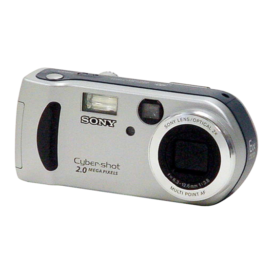
PHOTO DSC-P51
BLOCK DIAGRAMS
BLOCK DIAGRAMS
FRAME SCHEMATIC DIAGRAMS
FRAME SCHEMATIC DIAGRAMS
SCHEMATIC DIAGRAMS
SCHEMATIC DIAGRAMS
Canadian Model
AEP Model
Hong Kong Model
Australian Model
Chinese Model
Korea Model
Tourist Model
Japanese Model
PRINTED WIRING BOARDS
PRINTED WIRING BOARDS
ADJUSTMENTS
ADJUSTMENTS
REPAIR PARTS LIST
REPAIR PARTS LIST
DIGITAL STILL CAMERA
3
LEVEL
US Model
DSC-P51/P51M
UK Model
E Model
DSC-P51
Advertisement
Table of Contents


Need help?
Do you have a question about the DSC-P51M and is the answer not in the manual?
Questions and answers