Sony DSC-W55 Service Manual
Digital still camera
Hide thumbs
Also See for DSC-W55:
- Service manual (60 pages) ,
- Practical user's manual (114 pages) ,
- Handbook (111 pages)
Table of Contents
Advertisement
Quick Links
SERVICE MANUAL
Ver. 1.2 2007.06
Revision History
Revision History
How to use
How to use
Acrobat Reader
Acrobat Reader
Internal memory
Internal memory
ON BOARD
ON BOARD
Revised-1
Link
Link
SERVICE NOTE
SCHEMATIC DIAGRAMS
The components identified by
mark 0 or dotted line with
mark 0 are critical for safety.
Replace only with part num-
ber specified.
DSC-W55_L3
9-852-160-12
PRINTED WIRING BOARDS
Les composants identifiés par une
marque 0 sont critiques pour la
sécurité.
Ne les remplacer que par une pièce
portant le numéro spécifié.
Sony EMCS Co.
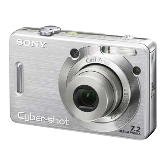
DSC-W55
Photo: Silver
DIGITAL STILL CAMERA
LEVEL
US Model
Canadian Model
AEP Model
UK Model
E Model
Australian Model
Hong Kong Model
Chinese Model
Korea Model
Argentine Model
Brazilian Model
Tourist Model
REPAIR PARTS LIST
Published by Kohda TEC
3
2007F0800-1
© 2007.06
Advertisement
Table of Contents

Related Manuals for Sony DSC-W55


Summary of Contents for Sony DSC-W55
- Page 1 0 are critical for safety. sécurité. Replace only with part num- Ne les remplacer que par une pièce ber specified. portant le numéro spécifié. DIGITAL STILL CAMERA 2007F0800-1 DSC-W55_L3 © 2007.06 Sony EMCS Co. 9-852-160-12 Published by Kohda TEC...
- Page 2 CRITIQUES POUR LA SÉCURITÉ DE FONCTIONNEMENT. NE COMPONENTS WITH SONY PARTS WHOSE PART NUMBERS REMPLACER CES COMPOSANTS QUE PAR DES PIÈSES SONY APPEAR AS SHOWN IN THIS MANUAL OR IN SUPPLEMENTS DONT LES NUMÉROS SONT DONNÉS DANS CE MANUEL OU PUBLISHED BY SONY.
-
Page 3: Table Of Contents
TABLE OF CONTENTS Section Title Page SERVICE NOTE 1-3. Method for Copying or Erasing the Data in Internal Memory ··········································································· 1-2 PRINTED WIRING BOARDS AND SCHEMATIC DIAGRAMS 4-2. Schematic Diagrams ························································ 4-3 4-3. Printed Wiring Boards ··················································· 4-16 4-4. Mounted Parts Location ················································ 4-24 REPAIR PARTS LIST 5-2. -
Page 4: Service Note
1. SERVICE NOTE 1-3. METHOD FOR COPYING OR ERASING THE DATA IN INTERNAL MEMORY The data can be copied/erased by the operations on the Setup screen. (When erasing the data, execute formatting the internal memory.) Note 1: When replacing the SY-176 board, erase the data in internal memory of the board before replacement. Note 2: When replacing the SY-176 board, execute formatting and initialize the internal memory after replacement. -
Page 5: Schematic Diagrams
4-2. SCHEMATIC DIAGRAMS Link Link SY-176 BOARD (1/6) SY-176 BOARD (4/6) (SDRAM, SUPER AND) (CCD SIGNAL PROCESS) SY-176 BOARD (2/6) (CAMERA DSP) SY-176 BOARD (5/6) (AUDIO, VIDEO) SY-176 BOARD (3/6) (LENS DRIVE) SY-176 BOARD (6/6) (DC/DC CONVERTER) COMMON NOTE FOR SCHEMATIC DIAGRAMS DSC-W55_L3... -
Page 6: Printed Wiring Boards And Schematic Diagrams
4-2. SCHEMATIC DIAGRAMS 4-2. SCHEMATIC DIAGRAMS 4. PRINTED WIRING BOARDS AND SCHEMATIC DIAGRAMS 4-2. SCHEMATIC DIAGRAMS THIS NOTE IS COMMON FOR SCHEMATIC DIAGRAMS (In addition to this, the necessary note is printed in each block) (For schematic diagrams) 1. Connection •... - Page 7 Ver. 1.1 2007.06 SY-176 BOARD(1/6) :Voltage measurement of the CSP ICs and the Transistors with mark, are not possible. CCD SIGNAL PROCESS XX MARK:NO MOUNT NO MARK:REC/PB MODE R318 R328 (2/6) R:REC MODE XIC101_1_SCK @001 (4/6) R317 R327 P:PB MODE IC101_1_SO (5/6) R316...
- Page 8 Ver. 1.1 2007.06 REG_GND SY-176 BOARD(2/6) DSP_DQ0 DSP_DQ0 CAMERA DSP CLKTGO DSP_DQ1 R193 CLKTGO DSP_DQ1 VSUB_CONT_POST DSP_DQ2 C115 Q102 DSP_DQ2 XX MARK:NO MOUNT 0.1u SSM6L16FE(TPLR3) VSUB_CONT_POST VSUB_CONT_PRE DSP_DQ3 BATTERY CHARGE VSUB_CONT_PRE DSP_DQ3 NO MARK:REC/PB MODE DETECT XCS_FE DSP_DQ4 XCS_FE DSP_DQ4 CA_HD DSP_DQ5 DSP_DQ5...
- Page 9 Ver. 1.1 2007.06 SY-176 BOARD(3/6) :Voltage measurement of the CSP ICs and the Transistors with mark, are LENS DRIVE not possible. XX MARK:NO MOUNT REG_GND D_3.2V A_3.2V (6/6) CN401 M_5V LENS_TENP XZM_RST_LED Z_PI_SENS_OUT ZM_DC_FG_1A R402 Z_PI_SENS_Vcc XZM_FG_LED XZM_RST_LED ZM_DC_FG_1B F_PI_SENS_OUT LENS_TEMP R401 390 F_PI_SENS_Vcc...
- Page 10 Ver. 1.1 2007.06 SY-176 BOARD(4/6) :Voltage measurement of the CSP ICs SDRAM, SUPER AND and the Transistors with mark, are not possible. XX MARK:NO MOUNT D_3.2V (6/6) M_5V D_1.8V REG_GND @011 XDD_RST_OUT XDD_RST_OUT DSP_AQ0 DSP_AQ0 DSP_AQ1 (6/6) DSP_AQ1 C210 C211 DSP_AQ2 C212 DSP_AQ2...
- Page 11 Ver. 1.1 2007.06 • Refer to page 4-3 for mark 0. SY-176 BOARD(5/6) :Voltage measurement of the CSP ICs and the Transistors with mark, are AUDIO, VIDEO not possible. XX MARK:NO MOUNT NO MARK:REC/PB MODE R608 2200 IC101_AUIN C617 C611 0.01u 0.022u M_5V...
- Page 12 Ver. 1.1 2007.06 • Refer to page 4-3 for mark 0. SY-176 BOARD(6/6) :Voltage measurement of the CSP ICs and the Transistors with mark, are not possible. DC/DC CONVERTER F001 XX MARK:NO MOUNT (1.25A/32V) (5/6) ACV_UNREG ST_UNREG NO MARK:REC/PB MODE (2/6) VL_3V R012...
-
Page 13: Printed Wiring Boards
4-3. PRINTED WIRING BOARDS Link Link SY-176 BOARD COMMON NOTE FOR PRINTED WIRING BOARDS MOUNTED PARTS LOCATION DSC-W55_L3... - Page 14 4-3. PRINTED WIRING BOARDS 4-3. PRINTED WIRING BOARDS 4-3. PRINTED WIRING BOARDS THIS NOTE IS COMMON FOR PRINTED WIRING BOARDS • : Uses unleaded solder. • Chip parts. Transistor Diode • : Circuit board : Flexible board Pattern from the side which enables seeing. : pattern of the rear side (The other layers’...
- Page 15 SY-176 (8 layers) : Uses unleaded solder. SY-176 BOARD (SIDE A) SY-176 BOARD (SIDE B) >EP GW< R606 C614 C619 R711 CN705 C003 R010 R007 C004 C006 C026 CN704 X001 Q701 R025 L009 R713 C618 FB301 C303 C023 R710 R607 R604 R315 LND704...
-
Page 16: Mounted Parts Location
4-3. PRINTED WIRING BOARDS 4-3. PRINTED WIRING BOARDS 4-4. MOUNTED PARTS LOCATION no mark : side A * mark : side B SY-176 BOARD C001 * C148 * CL305 LND704 A1 * R325 C002 * C149 * CL306 * R326 C003 * C208 * CL307... -
Page 17: Repair Parts List
5. REPAIR PARTS LIST NOTE: • -XX, -X mean standardized parts, so they may have some differences from When indicating parts by reference number, the original one. please include the board name. • Items marked “*” are not stocked since they are seldom required for routine The components identified by mark 0 or service. -
Page 18: Electrical Parts List
Ver. 1.1 2007.06 SY-176 5-2. ELECTRICAL PARTS LIST Ref. No. Part No. Description Ref. No. Part No. Description A-1231-207-A SY-176 BOARD, COMPLETE (SERVICE) (GP2) C116 1-125-777-11 CERAMIC CHIP 0.1uF A-1231-208-A SY-176 BOARD, COMPLETE (SERVICE) (GP3) A-1231-209-A SY-176 BOARD, COMPLETE (SERVICE) (GP4) C118 1-125-777-11 CERAMIC CHIP 0.1uF... - Page 19 Ver. 1.1 2007.06 SY-176 Ref. No. Part No. Description Ref. No. Part No. Description C602 1-125-837-91 CERAMIC CHIP 6.3V < FERRITE BEAD > C603 1-165-989-11 CERAMIC CHIP 10uF 6.3V C604 1-100-506-91 CERAMIC CHIP 6.3V FB101 1-469-580-11 INDUCTOR, FERRITE BEAD (1005) C605 1-125-837-91 CERAMIC CHIP 6.3V...
- Page 20 Ver. 1.1 2007.06 SY-176 Ref. No. Part No. Description Ref. No. Part No. Description < RESISTOR > R321 1-218-990-11 RES-CHIP 1/16W R322 1-218-941-81 RES-CHIP 1/16W R001 1-218-961-11 RES-CHIP 4.7K 1/16W R323 1-218-953-11 RES-CHIP 1/16W R002 1-218-985-11 RES-CHIP 470K 1/16W R325 1-218-990-11 RES-CHIP 1/16W R004...
- Page 21 SY-176 Board (1/6) SY-176 Board (1/6) Location: B-8 to C-10 Location: B-8 to C-10 R318 R328 R318 R317 R327 R317 R316 FB304 R316 FB304 R314 R326 R314 R313 R325 R313 2007F0800-1 DSC-W55_L3 ©2007.06 Sony EMCS Co. 9-852-160-83 Published by Kohda TEC...
- Page 22 : Points changed portion Page Suffix -11 Suffix -12 SY-176 Board (1/6) SY-176 Board (1/6) Location: E-12 to F-13 Location: E-12 to F-13 CA_AD01 CA_AD01 CL305 CL305 CA_AD00 CA_AD00 C326 C326 SCLK SCLK R323 R323 RESET RESET SDATA SDATA SOUT(CLPOB) CL306 SOUT(CLPOB) CL306...
- Page 23 : Points changed portion Page Suffix -11 Suffix -12 SY-176 Board (2/6) SY-176 Board (2/6) Location: Q-6 to R-8 Location: Q-6 to R-8 AA5 AB5 AF4 AC4 AE4 AE5 AC5 AB6 AF5 AF6 AF7 AC6 AB7 AE6 AB8 AC7 AB9 AE8 AA5 AB5 AF4 AC4 AE4 AE5 AC5 AB6 AF5 AF6 AF7 AC6 AB7 AE6 AB8 AC7 AB9 AE8 RB104 RB104...
- Page 24 : Points changed portion Page Suffix -11 Suffix -12 SY-176 Board (6/6) SY-176 Board (6/6) Location: H-5 to J-7 Location: H-5 to J-7 XRESET XRESET XPWROFF XPWROFF C006 C006 R008 R008 XPWRON1 XPWRON1 C007 C007 R009 R009 XPWRON2 XPWRON2 C001 C001 0.1u 0.1u...
- Page 25 : Points changed portion Page Suffix -11 Suffix -12 SY-176 Board SY-176 Board Location: Side A C-1 to D-1 Location: Side A C-1 to D-1 R702 R702 C704 C704 R707 R706 FB703 FB703 FB702 FB702 SY-176 Board SY-176 Board Location: Side B A-1 to B-2 Location: Side B A-1 to B-2 R315 C328...
- Page 26 : Points changed portion Page Suffix -11 Suffix -12 SY-176 Board SY-176 Board Location: Side B D-2 Location: Side B D-2 C135 C135 C133 R144 C133 R144 VIDEO_VCC VIDEO_VCC 4-18 D601 D601 C604 C603 C604 C603 5-2. ELECTRICAL PARTS LIST Page Suffix -11 Suffix -12...
- Page 27 [Description of main button functions on toolbar of the Adobe Acrobat Reader Ver5.0 (for Windows)] Toolbar Printing a text Reversing the screens displayed once • To reverse the previous screens (operation) one by one, click 1. Click the Print button 2.
-
Page 28: Revision History
Reverse 985216013.pdf Revision History S.M. Rev. Ver. Date History Contents issued 2007.01 Official Release — — 2007.06 Revised-1 • Addition of Note for Schematic Diagrams. S.M Correction : Page 4-6, 4-7, 4-8, 4-9, 4-10, 4-11, 5-8, 5-9, 5-10 2007.06 Supplement-1 •...
Need help?
Do you have a question about the DSC-W55 and is the answer not in the manual?
Questions and answers