Table of Contents
Advertisement
QQ
3 7 63 1515 0
SERVICE MANUAL
Ver 1.8 2003.12
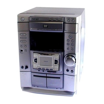
• HCD-DP1000D is the tuner, deck,
DVD and amplifier section in MHC-
DP1000D.
TE
L 13942296513
AUDIO POWER SPECIFICATIONS:
(USA model only)
POWER OUTPUT AND TOTAL
HARMONIC DISTORTION
with 8 ohm loads both channels driven, from
120 Hz – 10 kHz; rates 100 watts per channel
minimum RMS power, with no more than 10%
total harmonic distortion from 250 milliwatts to
rated output.
Continuous RMS power output
Center speaker:
Rear speakers:
Amplifier section
Canadian model:
Continuous RMS power output (reference)
Front speaker:
Center speaker:
Rear speakers:
Total harmonic distortion less than 0.07%
European model:
DIN power output (rated) 60 + 60 watts
Continuous RMS power output (reference)
www
Front speaker:
Center speaker:
Rear speakers:
.
Sony Corporation
9-873-314-09
Home Audio Company
2003L02-1
Published by Sony Engineering Corporation
© 2003.12
http://www.xiaoyu163.com
HCD-DP1000D
30 watts
30 + 30 watts
(8 ohms at 1 kHz, 10% THD)
100 + 100 watts
30 watts
30 + 30 watts
(8 ohms at 1 kHz, 10% THD)
(8 ohms at 1 kHz, 70 W)
(8 ohms at 1 kHz, DIN)
80 + 80 watts
x
ao
u163
30 watts
y
30 + 30 watts
(8 ohms at 1 kHz, 10% THD)
i
http://www.xiaoyu163.com
2 9
8
PHOTO :E model
Model Name Using Similar Mechanism
DVD
DVD Mechanism Type
Section
Base Unit Name
Optical Pick-up Name
Tape deck
Model Name Using Similar Mechanism
Section
Tape Transport Mechanism Type
Q Q
3
6 7
1 3
SPECIFICATIONS
Music power output (reference)
Front speaker:
Center speaker:
Rear speakers:
Other models:
The following measured at AC 120, 220, 240 V,
50/60 Hz
DIN power output (rated) 90 + 90 watts
Continuous RMS power output (reference)
Front speaker:
Center speaker:
Rear speakers:
Inputs
GAME IN:
(phono jacks)
MD (VIDEO) IN:
(phono jacks)
OPTICAL IN:
(Square optical connector jacks, front panel)
wavelength
MIC:
(Except for North
American and
European models)
(phone jack)
MINI HI-FI COMPONENT SYSTEM
.
9 4
2 8
US Model
Canadian Model
AEP Model
UK Model
Australian Model
NEW
CDM58D-DVBU9
DVBU9
KHM-240AAA/CLNP
HCD-DP800AV
TCM-230AWR41/MWR41
1 5
0 5
8
2 9
9 4
150 + 150 watts
60 watts
60 + 60 watts
(8 ohms at 1 kHz, 10% THD)
(8 ohms at 1 kHz, DIN)
120 + 120 watts
40 watts
40 + 40 watts
(8 ohms at 1 kHz, 10% THD)
voltage 250 mV,
impedance 47 kilohms
voltage 450 mV/250 mV,
impedance 47 kilohms
——
sensitivity 1 mV,
impedance 10 kilohms
— Continued on next page —
m
co
9 9
E Model
2 8
9 9
Advertisement
Table of Contents

Related Manuals for Sony HCD-DP1000D


Summary of Contents for Sony HCD-DP1000D
- Page 1 US Model Canadian Model AEP Model Ver 1.8 2003.12 UK Model E Model Australian Model • HCD-DP1000D is the tuner, deck, DVD and amplifier section in MHC- DP1000D. PHOTO :E model Model Name Using Similar Mechanism DVD Mechanism Type CDM58D-DVBU9...
- Page 2 Tuning range 87.5 – 108.0 MHz CRITIQUES POUR LA SÉCURITÉ DE FONCTIONNEMENT. NE Antenna FM lead antenna REMPLACER CES COMPOSANTS QUE PAR DES PIÈSES SONY Antenna terminals 75 ohm unbalanced DONT LES NUMÉROS SONT DONNÉS DANS CE MANUEL OU Intermediate frequency 10.7 MHz...
- Page 3 HCD-DP1000D 3 7 63 1515 0 Laser component in this product is capable SAFETY CHECK-OUT of emitting radiation exceeding the limit for (US model only) Class 1. After correcting the original service problem, perform the following safety checks before releasing the set to the customer: Check the antenna terminals, metal trim, “metallized”...
-
Page 4: Table Of Contents
6-17.Printed Wiring Board DSP Section ·························· 40 dealer or local authorized 6-18. Schematic Diagram DSP Section (1/2) ··················· 41 Sony service facility and give 6-19. Schematic Diagram DSP Section (2/2) ··················· 42 the 5-character service 6-20. Printed Wiring Board OPT/VIDEO Section ··········· 43 number. - Page 5 HCD-DP1000D Ver 1.6 2003.01 3 7 63 1515 0 SERVICE POSITION MB board Jig (J-2501-155-A) to RF240 board : CN004 Jig (J-2501-199-A) to RF240 board : CN002 L 13942296513 CHANGE OF OPTICAL PICK-UP Optical Pick-up has been replaced from KHM-240AAA (TYPE A) to KHM-270AAA (TYPE B) from the middle of production.
-
Page 6: General
HCD-DP1000D Ver 1.3 2002.07 This section is extracted from SECTION 1 3 7 63 1515 0 instruction manual. GENERAL Parts Identification The items are arranged in alphabetical order. Main unit ea esedefegeh rgrf rdrs 2CH/MULTI rs (24, 46) MIC LEVEL control (Except for... -
Page 7: Disassemby
HCD-DP1000D SECTION 2 3 7 63 1515 0 DISASSEMBLY • The equipment can be removed using the following procedure. Case (Top) Loading Panel Front Panel Section Tape Mechanism Deck LEAF SW board, Head (A) board, Head (B) board (TCM-230AWR41/MWR41) - Page 8 HCD-DP1000D 3 7 63 1515 0 2-2. LOADING PANEL 4 pull-out the disc tray. DVD mechanism deck (CDM58D) 1 turn the pulley to the direction of arrow. loading panel front panel side pulley 2 pull-out the disc tray. L 13942296513 2-3.
- Page 9 HCD-DP1000D 3 7 63 1515 0 2-4. TAPE MECHANISM DECK (TCM-230AWR41/MWR41) 1 four screws (+BVTP 2.6 × 8) 2 tape mechanism deck (TCM-230AWR41/MWR41) L 13942296513 2-5. CD PANEL BOARD, PANEL BOARD, OPT IN BOARD 1 five screws (+BVTP 2.6 × 8)
- Page 10 HCD-DP1000D 3 7 63 1515 0 2-6. ESCUTCHEON PAD (WITH TOUCH PAD) 1 button (edit) 6 two screws (TPG +P 2 × 8) 8 three screws 3 two screws (+BVTP 2.6 × 8) (+BVTP 2.6 × 8) 9 button (DSP) 2 two screws (+BVTP 2.6 ×...
- Page 11 HCD-DP1000D 3 7 63 1515 0 2-8. TRANS BOARD, MAIN BOARD 8 two screws 4 two screws 6 TRANS board (+BVTP 3 × 8) (+BVTT 4 × 8) 5 two screws 7 two screws (+BVTT 4 × 8) (+BVTT 3 × 8)
- Page 12 HCD-DP1000D 3 7 63 1515 0 2-10. LEAF SW BOARD, HEAD (A) BOARD, HEAD (B) BOARD (TCM-230AWR41/MWR41) Note: This illustration is for TCM-230MWR, but in case of TCM-230AWR, you can remove them in the same way. 1 five claws 2 LEAF SW board 3 remove the four solderings.
- Page 13 HCD-DP1000D 3 7 63 1515 0 2-12. RF-240 BOARD, OPTICAL PICK-UP (KHM-240AAA) qd optical pick-up (KHM-240AAA) 7 step screw (L) 0 insulator 9 step screw (10) 5 flat type wire (26 core) 6 flat type wire (9 core) qs insulator...
-
Page 14: Test Mode
HCD-DP1000D SECTION 3 TEST MODE 3 7 63 1515 0 [Cold Reset] [MC Test Mode] • The cold reset clears all data including preset data stored in the • This mode is used to check operations of the respective sections RAM to initial conditions. - Page 15 HCD-DP1000D 3 7 63 1515 0 [Aging Mode] This mode can for operation check of tape deck section and DVD section. • If an error occurred: The aging operation stops and display then status. • If no error occurs: The aging operation continues repeatedly.
- Page 16 HCD-DP1000D 3 7 63 1515 0 [DVD Section] 2. CDM Error History <CDM58D Error History Display> • The sequence during the aging mode is following as below. 11 digits are displayed after the M character. Aging mode sequence (DVD section):...
-
Page 17: Mechanical Adjustments
HCD-DP1000D SECTION 4 3 7 63 1515 0 MECHANICAL ADJUSTMENTS [VACS ON/OFF MODE] Precaution • This mode is used to switch ON and OFF the VACS (Variable 1. Clean the following parts with a denatured alcohol-moistened Attenuation Control System). -
Page 18: Electrical Adjustments
HCD-DP1000D SECTION 5 3 7 63 1515 0 ELECTRICAL ADJUSTMENTS 2. Turn the adjustment screw and check output peaks. If the peaks DECK SECTION 0 dB=0.775 V do not match for L-CH and R-CH, turn the adjustment screw so that outputs match within 1dB of peak. - Page 19 HCD-DP1000D 3 7 63 1515 0 DECK B REC Bias Adjustment DECK B Tape Speed Adjustment Procedure: Note: Start the Tape Speed adjustment as below after setting to the test mode. INTRODUCTION In the test mode, the tape speed is high during pressing the...
- Page 20 HCD-DP1000D 3 7 63 1515 0 FM Tuned Level Adjustment 4. Mode: Record FM RF SSG MD/VIDEO (AUDIO) IN 75 Ω coaxial 315 Hz, 50 mV (–23.8 dB) AF OSC blank tape 600 Ω CS-123 attenuator Carrier frequency : 98 MHz...
-
Page 21: Diagrams
HCD-DP1000D Ver 1.7 2003.02 SECTION 6 3 7 6 3 1 5 1 5 0 DIAGRAMS Oscilloscope DVD SECTION 75 Ω THIS NOTE IS COMMON FOR PRINTED WIRING BOARDS AND SCHEMATIC DIAGRAMS. RE-ADJUSTMENT OF THE SERVO CIRCUIT (In addition to this, the necessary note is printed in each block.) -
Page 22: Circuit Board Location
HCD-DP1000D 3 7 6 3 1 5 1 5 0 6-1. CIRCUIT BOARD LOCATION WAVEFORMS – PF-240 BOARD – – MAIN BOARD – – MB BOARD – IC001 2 RFIN IC701 2 INA NO303 8 E-HOT IC102 8 XTO... -
Page 23: Block Diagrams
HCD-DP1000D 3 7 6 3 1 5 1 5 0 6-2. BLOCK DIAGRAMS – TUNER/DVD DSP SECTION – DIGITAL SERVO DIGITAL SIGNAL PROCESSOR OPTICAL PICK-UP DIGITAL AUDIO D/A CONV. BLOCK IC001 INTERFACE IC302 (1/2) (KHM-240AAA) RF AMP IC604 (2/2) - Page 24 HCD-DP1000D 3 7 6 3 1 5 1 5 0 – DVD SYS SECTION – TRST IC302 (2/2) IC503 (2/2) DIGFITAL SERVO MPEG DECODER DIGITAL SIGNAL PROCESSOR D/A CONV. XSRQ IREQO IC006 +1.8V HAD0-7 +1.8V D0-7 A0-7 HD0-7 218-215,213-210...
- Page 25 HCD-DP1000D 3 7 6 3 1 5 1 5 0 – MAIN SECTION – J601 L REC OUT IC607(1/2) IC1001 RY1082 TM1001 SOUND PROCESSOR R-CH CENTER IC1201 COUT SPEAKR MD VIDEO Q610 L IN1 J1202 MUTE MAC IN POWER...
- Page 26 HCD-DP1000D 3 7 6 3 1 5 1 5 0 6-3. PRINTED WIRING BOARD – RF-240 SECTION – • See page 22 for Circuit Boards Location. RF–240 BOARD (SIDE A) RF–240 BOARD (SIDE B) BOARD OPTICAL (Page 28) PICK–UP BLOCK KHM–240AAA...
- Page 27 HCD-DP1000D 3 7 6 3 1 5 1 5 0 6-4. SCHEMATIC DIAGRAM – RF-240 SECTION – • See page 22 for Waveforms. • See page 64 for IC Block Diagrams. 1 3 9 4 2 2 9 6 5 1 3...
-
Page 28: Mb Section
HCD-DP1000D 3 7 6 3 1 5 1 5 0 6-5.PRINTED WIRING BOARD – MB SECTION – • See page 22 for Circuit Boards Location. RF–240 RF–240 BOARD BOARD MB BOARD (SIDE A) (Page 26) (Page 26) • Semiconductor Location Ref. - Page 29 HCD-DP1000D Ver 1.6 2003.01 3 7 6 3 1 5 1 5 0 MB BOARD (SIDE B) • Semiconductor Location Ref. No. Location IC101 IC102 IC106 IC107 IC301 IC303 IC401 IC501 IC502 IC504 IC505 IC701 Q711 Q712 1 3 9 4 2 2 9 6 5 1 3...
-
Page 30: Schematic Diagram
HCD-DP1000D Ver 1.6 2003.01 3 7 6 3 1 5 1 5 0 6-6. SCHEMATIC DIAGRAM – MB(1/5) SECTION – 1 3 9 4 2 2 9 6 5 1 3 w w w u 1 6 3 http://www.xiaoyu163.com... -
Page 31: Mb Section (2/5)
HCD-DP1000D 3 7 6 3 1 5 1 5 0 6-7. SCHEMATIC DIAGRAM – MB(2/5) SECTION – • See page 61 for IC Block Diagrams. 1 3 9 4 2 2 9 6 5 1 3 w w w u 1 6 3 http://www.xiaoyu163.com... -
Page 32: Schematic Diagram
HCD-DP1000D 3 7 6 3 1 5 1 5 0 6-8. SCHEMATIC DIAGRAM – MB(3/5) SECTION – 1 3 9 4 2 2 9 6 5 1 3 w w w u 1 6 3 http://www.xiaoyu163.com... -
Page 33: Mb Section (4/5)
HCD-DP1000D 3 7 6 3 1 5 1 5 0 6-9. SCHEMATIC DIAGRAM – MB(4/5) SECTION – • See page 22 for Waveforms. • See page 61 for IC Block Diagrams. • See page 54 for IC Pin Function. -
Page 34: Mb Section (5/5)
HCD-DP1000D 3 7 6 3 1 5 1 5 0 6-10. SCHEMATIC DIAGRAM – MB(5/5) SECTION – • See page 22 for Waveforms. • See page 63 for IC Block Diagrams. 1 3 9 4 2 2 9 6 5 1 3... -
Page 35: Driver Section
HCD-DP1000D 3 7 6 3 1 5 1 5 0 6-11. SCHEMATIC DIAGRAM – DRIVER SECTION – 1 3 9 4 2 2 9 6 5 1 3 6-12.PRINTED WIRING BOARD – DRIVER SECTION – • See page 22 for Circuit Boards Location. -
Page 36: Main Section
HCD-DP1000D 3 7 6 3 1 5 1 5 0 6-13. PRINTED WIRING BOARD – MAIN SECTION – • See page 22 for Circuit Boards Location. • Semiconductor Location Ref. No. Location BOARD MAIN BOARD (Page 40) D111 D112... -
Page 37: Main Section (1/3)
HCD-DP1000D 3 7 6 3 1 5 1 5 0 6-14. SCHEMATIC DIAGRAM – MAIN (1/3) SECTION – • See page 22 for Waveforms. • See page 61 for IC Block Diagrams. 1 3 9 4 2 2 9 6 5 1 3... -
Page 38: Main Section (2/3)
HCD-DP1000D 3 7 6 3 1 5 1 5 0 6-15. SCHEMATIC DIAGRAM – MAIN (2/3) SECTION – • See page 22 for Waveforms. • See page 56 for IC Pin Function. 1 3 9 4 2 2 9 6 5 1 3... -
Page 39: Main Section (3/3)
HCD-DP1000D 3 7 6 3 1 5 1 5 0 6-16. SCHEMATIC DIAGRAM – MAIN (3/3) SECTION – • See page 22 for Waveforms. • See page 62,63 for IC Block Diagrams. 1 3 9 4 2 2 9 6 5 1 3... -
Page 40: Dsp Section
HCD-DP1000D 3 7 6 3 1 5 1 5 0 6-17. PRINTED WIRING BOARD – DSP SECTION – • See page 22 for Circuit Boards Location. MAIN BOARD DSP BOARD (SIDE A) DSP BOARD (SIDE B) (Page 36) R761... -
Page 41: Dsp Section (1/2)
HCD-DP1000D 3 7 6 3 1 5 1 5 0 6-18. SCHEMATIC DIAGRAM – DSP (1/2) SECTION – • See page 59 for IC Pin Function. • See page 62 for IC Block Diagrams. 1 3 9 4 2 2 9 6 5 1 3... -
Page 42: Dsp Section (2/2)
HCD-DP1000D 3 7 6 3 1 5 1 5 0 6-19. SCHEMATIC DIAGRAM – DSP (2/2) SECTION – • See page 63 for IC Block Diagrams. 1 3 9 4 2 2 9 6 5 1 3 w w w u 1 6 3 http://www.xiaoyu163.com... -
Page 43: Opt/Video Section
HCD-DP1000D 3 7 6 3 1 5 1 5 0 6-20. PRINTED WIRING BOARD – OPT SECTION – • See page 22 for Circuit Boards Location. VIDEO BOARD • Semiconductor Location OPT IN BOARD Ref. No. Location D601 D602... -
Page 44: Front Amp Section
HCD-DP1000D 3 7 6 3 1 5 1 5 0 6-22. PRINTED WIRING BOARD – FRONT AMP SECTION – • See page 22 for Circuit Boards Location. SURROUND AMP MAIN SURROUND AMP MAIN BOARD BOARD BOARD BOARD (Page 46) -
Page 45: Front Amp Section
HCD-DP1000D 3 7 6 3 1 5 1 5 0 6-23. SCHEMATIC DIAGRAM – FRONT AMP SECTION – 1 3 9 4 2 2 9 6 5 1 3 w w w u 1 6 3 http://www.xiaoyu163.com... -
Page 46: Surround Amp Section
HCD-DP1000D 3 7 6 3 1 5 1 5 0 6-24. PRINTED WIRING BOARD – SURROUND AMP SECTION – • See page 22 for Circuit Boards Location. FRONT AMP FRONT AMP MAIN BOARD BOARD BOARD (Page 44) (Page 44) -
Page 47: Surround Amp Section
HCD-DP1000D 3 7 6 3 1 5 1 5 0 6-25. SCHEMATIC DIAGRAM – SURROUND AMP SECTION – 1 3 9 4 2 2 9 6 5 1 3 w w w u 1 6 3 http://www.xiaoyu163.com... -
Page 48: Panel Section
HCD-DP1000D 3 7 6 3 1 5 1 5 0 6-26. PRINTED WIRING BOARD – PANEL SECTION – • See page 22 for Circuit Boards Location. • Semiconductor Location Ref. No. Location D1114 D1115 D1116 D1117 Q1114 Q1115 Q1116 PANEL BOARD >... -
Page 49: Panel Section (1/2)
HCD-DP1000D 3 7 6 3 1 5 1 5 0 6-27. SCHEMATIC DIAGRAM – PANEL (1/2) SECTION – • See page 22 for Waveforms. • See page 58 for IC Pin Function. 1 3 9 4 2 2 9 6 5 1 3... -
Page 50: Panel Section (2/2)
HCD-DP1000D 3 7 6 3 1 5 1 5 0 6-28. SCHEMATIC DIAGRAM – PANEL (2/2) SECTION – 1 3 9 4 2 2 9 6 5 1 3 w w w u 1 6 3 http://www.xiaoyu163.com... -
Page 51: Leaf Sw Section
HCD-DP1000D 3 7 6 3 1 5 1 5 0 6-29. PRINTED WIRING BOARD – LEAF SW SECTION – • See page 22 for Circuit Boards Location. 6-30. SCHEMATIC DIAGRAM – LEAF SW SECTION – 1SS119-25 (Page 36) (Page 37) -
Page 52: Trans Section
HCD-DP1000D 3 7 6 3 1 5 1 5 0 6-31. PRINTED WIRING BOARD – TRANS SECTION – • See page 22 for Circuit Boards Location. • Semiconductor E C B T911 Location POWER TRANSFORMER Ref. No. Location D911... -
Page 53: Trans Section
HCD-DP1000D 3 7 6 3 1 5 1 5 0 6-32. SCHEMATIC DIAGRAM – TRANS SECTION – 1 3 9 4 2 2 9 6 5 1 3 w w w u 1 6 3 http://www.xiaoyu163.com... -
Page 54: Ic Pin Function Description
HCD-DP1000D 3 7 6 3 1 5 1 5 0 6-33. IC PIN FUNCTION DESCRIPTION • IC103 MB91307APFV-G-BND-E1 DVD SYSTEM CONTROL (MB BOARD (4/5)) Pin No. Pin No. Pin Name Description Pin Name Description XIFCS XIFCS signal output to M30622MGA... - Page 55 HCD-DP1000D 3 7 63 1515 0 Pin No. Pin Name Description Ground — Address bus to SRAM Address bus to SRAM Address bus to SRAM Address bus to SRAM Address bus to SRAM Address bus to SRAM Address bus to SRAM Address bus to SRAM Power supply +3.3V...
- Page 56 HCD-DP1000D 3 7 63 1515 0 • IC401 MASTER CONTROL (M30622MGA-A72FP) (MAIN Board (2/3)) Pin No. Pin Name Description AMP-DATA Amp data signal output AMP-CLK Amp clock signal output AMP-LAT Amp latch signal output SIRCS Remote commander signal input...
- Page 57 HCD-DP1000D 3 7 63 1515 0 Pin No. Pin Name Description NO-USE Not used B TRG B deck trigger control signal output AMS-IN AMS signal input CAPM-H/L Capstan moter highi/low speed control signal output CAPM-CNT 1 Capstan moter REV/FWD/STOP control signal output...
- Page 58 HCD-DP1000D 3 7 63 1515 0 • IC1101 DISPLAY CONTROL (MB90M407APF-G-115-BND) (PANEL Board (1/2)) Discription Pin No. Pin Name FIP/LED16 Grid drive signal output to the fluorescent indicator 2 to 5 FIP17 - 20 Grid drive signal output to the fluorescent indicator...
- Page 59 HCD-DP1000D 3 7 63 1515 0 • IC601 DECODER (CXD9617R) (DSP Board (1/2)) Description Pin No. Pin Name — Ground XRST Reset signal input EXTIN — Sampling frequency switching signal input (Not used) VDDI Power supply Sampling frequency switching signal input (Not used)
- Page 60 HCD-DP1000D 3 7 63 1515 0 Description Pin No. Pin Name MOD0 Operation mode signal input (Not used) EXLOCK Lock signal input VDDI Power supply — Ground 62, 63 A17, A16 External memory address output (SRAM) (Not used) 64 to 66...
-
Page 61: Ic Block Diagrams
HCD-DP1000D 3 7 63 1515 0 6-34. IC BLOCK DIAGRAMS IC302 CXD9635R (MB BOARD (2/5)) XDSRRST TESTK2 TESTK1 TESTK0 BOUNDARY SCAN VRTA VRTA VDDA0_3.3V A+3.3V TESTAA VSSA0 VDD_3.3V D+3.3V VRBA VRBA VSSD0 DA I/F PDM SERVO DSP VDD0_3.3V A+3.3V... - Page 62 HCD-DP1000D 3 7 63 1515 0 IC605 AK4527 (DSP BOARD (1/2)) IC81 BU1924 (MAIN BOARD (3/3)) 44 43 42 41 40 39 38 37 36 35 34 AUDIO CLOCK TEST MCLK DZF2 RIN+ SDTO SDOUT RIN– DEFFERENTIAL BIPHASE PLL 57KHz LIN–...
- Page 63 HCD-DP1000D 3 7 63 1515 0 IC11 LA1845 (MAIN BOARD (3/3)) RF.AMP DECODER PILOT BUFF ANTI-BRIDIE CANCEL P-DET STEREO φ LEVEL AM/FM COMP S-CURVE PILOT π BUFF 304KHz 19K∠ 19K∠0 TUNING DRIVE IC701 BA7666FS-E2 (MB BOARD (5/5)) MUTE BIAS 75Ω...
- Page 64 HCD-DP1000D 3 7 63 1515 0 IC001 SP3728AC (RF-240 BOARD) FULL WAVE CHARG RF IF INPUT PUMP RF IN SDEN BUTTOM SELIAL SCLK PORT DECODER INPUT PROGRAMBLE EQ.FILTER CONTROL SIG CLAMP HOLD – HOLD LEVEL RF HOLD EN RF AGC HOLD –...
-
Page 65: Exploded Views
HCD-DP1000D SECTION 7 EXPLODED VIEWS 3 7 63 1515 0 NOTE: • -XX, -X mean standardized parts, so they may • Hardware (# mark) list and accessories are The components identified by have some differences from the original one. -
Page 66: Front Panel Section
HCD-DP1000D Ver 1.8 3 7 63 1515 0 7-2. FRONT PANEL SECTION Tape mechanism deck FL1101 not supplied supplied not supplied L 13942296513 Supplied with S1101 Ref. No. Part No. Description Remarks Ref. No. Part No. Description Remarks 4-231-804-01 KNOB (VOL) -
Page 67: Chassis Section
HCD-DP1000D 3 7 63 1515 0 7-3. CHASSIS SECTION not supplied not supplied not supplied T911 not supplied L 13942296513 not supplied The components identified by mark 0 or dotted line with mark 0 are critical for safety. Replace only with part number specified. -
Page 68: Tape Mechanism Deck Section-1 (Tcm-230Mwr41)
HCD-DP1000D 3 7 63 1515 0 7-4. TAPE MECHANISM DECK SECTION-1 (TCM-230MWR41) • The thing that a part A curves is TCM-230MWR41. Note: Two different types of tape mechanism are used depending on models. They maintain compatibility as an entire mechanism even though there are some different parts are used. -
Page 69: Tape Mechanism Deck Section-2 (Tcm-230Awr41)
HCD-DP1000D 3 7 63 1515 0 7-5. TAPE MECHANISM DECK SECTION-2 (TCM-230AWR41) • The thing that a part A doesn’t curve is TCM-230AWR41. Note: Two different types of tape mechanism are used depending on models. They maintain compatibility as an entire mechanism even though there are some different parts are used. -
Page 70: Dvd Mechanism Deck Section (Cdm58D-Dvbu9)
HCD-DP1000D Ver 1.6 2003.01 3 7 63 1515 0 7-6. DVD MECHANISM DECK SECTION (CDM58D-DVBU9) M721 supplied L 13942296513 The components identified by mark 0 or dotted line with mark 0 are critical for safety. Replace only with part number specified. -
Page 71: Electrical Parts List
HCD-DP1000D SECTION 8 Ver 1.6 2003.01 ELECTRICAL PARTS LIST CD PANEL DIODE 3 7 63 1515 0 NOTE: Ref. No. Part No. Description Remarks Ref. No. Part No. Description Remarks • Due to standardization, replacements in the • COILS... - Page 72 HCD-DP1000D 3 7 63 1515 0 Ref. No. Part No. Description Remarks Ref. No. Part No. Description Remarks C623 1-126-934-11 ELECT 220uF C685 1-126-964-11 ELECT 10uF C624 1-164-156-11 CERAMIC CHIP 0.1uF C686 1-126-933-11 ELECT 100uF C625 1-162-915-11 CERAMIC CHIP 10PF 0.5PF...
- Page 73 HCD-DP1000D 3 7 63 1515 0 Ref. No. Part No. Description Remarks Ref. No. Part No. Description Remarks < DIODE > Q606 8-729-141-73 TRANSISTOR 2SC3624A-T1L15L16 Q607 8-729-141-73 TRANSISTOR 2SC3624A-T1L15L16 D601 8-719-158-02 DIODE RD3.9SB2 Q608 8-729-141-73 TRANSISTOR 2SC3624A-T1L15L16 D604 8-719-988-61 DIODE 1SS355TE-17...
- Page 74 HCD-DP1000D FRONT AMP 3 7 63 1515 0 Ref. No. Part No. Description Remarks Ref. No. Part No. Description Remarks R662 1-216-809-11 METAL CHIP 1/16W R728 1-216-845-11 METAL CHIP 100K 1/16W R663 1-216-817-11 METAL CHIP 1/16W R729 1-216-825-11 METAL CHIP 2.2K...
- Page 75 HCD-DP1000D FRONT AMP 3 7 63 1515 0 Ref. No. Part No. Description Remarks Ref. No. Part No. Description Remarks < CAPACITOR > C920 1-126-956-91 ELECT 0.1uF C921 1-128-582-11 ELECT 10uF 100V C801 1-128-582-11 ELECT 10uF 100V (US,CND) (US,CND)
- Page 76 HCD-DP1000D FRONT AMP HEAD (A) HEAD (B) LEAF SW 3 7 63 1515 0 Ref. No. Part No. Description Remarks Ref. No. Part No. Description Remarks < RESISTOR > R883 1-260-076-11 CARBON 1/2W R884 1-260-076-11 CARBON 1/2W R801 1-249-417-11 CARBON...
- Page 77 HCD-DP1000D LEAF SW MAIN 3 7 63 1515 0 Ref. No. Part No. Description Remarks Ref. No. Part No. Description Remarks R1005 1-247-818-11 CARBON 1/4W 1-162-974-11 CERAMIC CHIP 0.01uF R1006 1-247-864-11 CARBON 1/4W 1-126-962-11 ELECT 3.3uF R1007 1-247-780-00 CARBON...
- Page 78 HCD-DP1000D MAIN 3 7 63 1515 0 Ref. No. Part No. Description Remarks Ref. No. Part No. Description Remarks C171 1-107-721-11 ELECT 4.7uF 100V C362 1-162-968-11 CERAMIC CHIP 0.0047uF 10% C271 1-162-974-11 CERAMIC CHIP 0.01uF C363 1-162-968-11 CERAMIC CHIP 0.0047uF 10%...
- Page 79 HCD-DP1000D MAIN 3 7 63 1515 0 Ref. No. Part No. Description Remarks Ref. No. Part No. Description Remarks CN102 1-573-847-11 CONNECTOR, BOARD TO BOARD 15P < JUMPER RESISTOR > CN103 1-573-847-11 CONNECTOR, BOARD TO BOARD 15P CN104 1-564-518-11 PLUG, CONNECTOR 3P...
- Page 80 HCD-DP1000D MAIN 3 7 63 1515 0 Ref. No. Part No. Description Remarks Ref. No. Part No. Description Remarks 8-729-620-05 TRANSISTOR 2SC2603-EF 1-216-849-11 METAL CHIP 220K 1/16W 8-729-620-05 TRANSISTOR 2SC2603TP-EF (AEP,UK) 1-216-827-11 METAL CHIP 3.3K 1/16W 1-216-864-11 METAL CHIP...
- Page 81 HCD-DP1000D MAIN 3 7 63 1515 0 Ref. No. Part No. Description Remarks Ref. No. Part No. Description Remarks R313 1-216-845-11 METAL CHIP 100K 1/16W R388 1-216-837-11 METAL CHIP 1/16W R315 1-216-833-11 METAL CHIP 1/16W R389 1-216-834-11 METAL CHIP...
- Page 82 HCD-DP1000D MAIN 3 7 63 1515 0 Ref. No. Part No. Description Remarks Ref. No. Part No. Description Remarks R482 1-216-809-11 METAL CHIP 1/16W RV354 1-241-768-11 RES, ADJ, CARBON 220K (REC BIAS (R)) R483 1-216-809-11 METAL CHIP 1/16W R484...
- Page 83 HCD-DP1000D 3 7 63 1515 0 Ref. No. Part No. Description Remarks Ref. No. Part No. Description Remarks C312 1-107-826-11 CERAMIC CHIP 0.1uF C505 1-117-370-11 CERAMIC CHIP 10uF C313 1-164-677-11 CERAMIC CHIP 0.033uF C506 1-117-370-11 CERAMIC CHIP 10uF C315...
- Page 84 HCD-DP1000D Ver 1.6 2003.01 3 7 63 1515 0 Ref. No. Part No. Description Remarks Ref. No. Part No. Description Remarks CN404 1-793-687-11 PIN, CONNECTOR (1.5MM) (SMD)5P R077 1-216-815-11 METAL CHIP 1/10W (TYPE A) < FERRITE BEAD > R077...
- Page 85 HCD-DP1000D 3 7 63 1515 0 Ref. No. Part No. Description Remarks Ref. No. Part No. Description Remarks R154 1-216-833-11 METAL CHIP 1/16W R334 1-218-871-11 METAL CHIP 0.5% 1/10W (E91) R335 1-218-855-11 METAL CHIP 2.2K 0.5% 1/10W R336 1-216-833-11 METAL CHIP...
- Page 86 HCD-DP1000D Ver 1.1 2002.03 MOTOR OPT IN PANEL 3 7 63 1515 0 Ref. No. Part No. Description Remarks Ref. No. Part No. Description Remarks R524 1-216-833-11 METAL CHIP 1/16W A-4727-155-A PANEL BOARD, COMPLETE (including CD R525 1-216-833-11 METAL CHIP...
- Page 87 HCD-DP1000D PANEL 3 7 63 1515 0 Ref. No. Part No. Description Remarks Ref. No. Part No. Description Remarks C1213 1-126-157-11 ELECT 10uF Q1113 8-729-119-78 TRANSISTOR 2SC2785-HFE (AUS,E,E91,EA,MX,SP,MY,TH) Q1120 8-729-119-78 TRANSISTOR 2SC2785-HFE C1214 1-126-157-11 ELECT 10uF Q1123 8-729-029-94 TRANSISTOR DTC143TSA...
- Page 88 HCD-DP1000D PANEL 3 7 63 1515 0 Ref. No. Part No. Description Remarks Ref. No. Part No. Description Remarks R1163 1-249-424-11 CARBON 3.9K 1/4W F R1285 1-249-417-11 CARBON 1/4W F R1164 1-249-426-11 CARBON 5.6K 1/4W R1286 1-249-417-11 CARBON 1/4W F...
- Page 89 HCD-DP1000D RF-240 SENSOR SUB TRANS 3 7 63 1515 0 Ref. No. Part No. Description Remarks Ref. No. Part No. Description Remarks A-4726-861-A RF-240 MOUNTED BOARD, COMPLETE < RESISTOR > **************************** R002 1-216-809-11 METAL CHIP 1/16W < CAPACITOR >...
- Page 90 HCD-DP1000D SUB TRANS SURROUND AMP 3 7 63 1515 0 Ref. No. Part No. Description Remarks Ref. No. Part No. Description Remarks D902 8-719-024-99 DIODE 11ES2-NTA2B C1003 1-162-286-31 CERAMIC 220PF D903 8-719-024-99 DIODE 11ES2-NTA2B C1004 1-126-947-11 ELECT 47uF D904...
- Page 91 HCD-DP1000D SURROUND AMP TRANS 3 7 63 1515 0 Ref. No. Part No. Description Remarks Ref. No. Part No. Description Remarks 0 R1055 Q1001 8-729-140-84 TRANSISTOR 2SC1841-PAFAEA 1-220-755-11 METAL 0.22 Q1016 8-729-140-84 TRANSISTOR 2SC1841-PAFAEA 0 R1056 Q1017 8-729-119-78 TRANSISTOR 2SC2785-HFE 1-220-755-11 METAL 0.22...
- Page 92 HCD-DP1000D Ver 1.6 2003.01 TRANS VIDEO 3 7 63 1515 0 Ref. No. Part No. Description Remarks Ref. No. Part No. Description Remarks < DIODE > MISCELLANEOUS ************* D911 8-719-024-99 DIODE 11ES2-NTA2B D912 8-719-983-88 DIODE MTZJ-T-72-33C 1-823-367-11 WIRE (FLAT TYPE) (9 CORE) D913 8-719-118-56 DIODE RD4.7F-T7B1...
- Page 93 HCD-DP1000D 3 7 63 1515 0 US Model Canadian Model SERVICE MANUAL AEP Model UK Model Ver 1.5 2002.10 E Model Australian Model SUPPLEMENT-1 File this supplement with the service manual. Subject: 1. DVD test Mode L 13942296513 u163 9-873-314-81 http://www.xiaoyu163.com...
- Page 94 HCD-DP1000D 3 7 63 1515 0 TEST MODE ### Syscon Diagnosis ### 1-1. GENERAL DESCRIPTION Diag All Check The Test Mode allows you to make diagnosis and adjustment eas- No. 2 Version ily using the remote commander and monitor TV. The instructions, diagnostic results, etc.
- Page 95 HCD-DP1000D 3 7 63 1515 0 4. Servo Selecting 2 and subsequent items executes respective menus and outputs the results. For the contents of each submenu, see “Check Items List”. (4-2) Servo DSP Check Data write → read, and accord check...
- Page 96 HCD-DP1000D 3 7 63 1515 0 6. AV Decoder (5-4) ARP to RAM Address Bus Data write → other address read discord check Error 10: ARP → RAM address bus error (6-2) 1930 RAM Caution: Address and data display in case of an error is Data write →...
- Page 97 HCD-DP1000D 3 7 63 1515 0 Check Items List Error Codes List 00: Error not detected 01: RAM write/read data discord 2) Version 02: Gate array NG (2-2) Revision 03: EEPROM NG (2-3) ROM Check Sum 08: ARP register read data discord (2-4) Model Type 09: ARP ←→...
- Page 98 HCD-DP1000D 3 7 63 1515 0 1-4. DRIVE AUTO ADJUSTMENT 1. DVD-SL (single layer) [ENTER] Select , insert DVD single layer disc, and press key, On the Test Mode Menu screen, press key on the remote com- and the adjustment will be made through the following steps, then mander, and the Adjustment Menu will be displayed.
- Page 99 HCD-DP1000D 3 7 63 1515 0 2. CD 3. DVD-DL (dual layer) [ENTER] [ENTER] Select , insert CD disc, and press key, and the adjust- Select , insert DVD dual layer disc, and press key, ment will be made through the following steps, then adjusted val- and the adjustment will be made through the following steps, then ues will be written to the EEPROM.
- Page 100 HCD-DP1000D 3 7 63 1515 0 4. SACD 1-5. DRIVE MANUAL OPERATION [ENTER] Select , insert SACD disc, and press key, and the On the Test Mode Menu screen, select , and the Operation Menu adjustment will be made through the following steps, then adjusted will be displayed.
- Page 101 HCD-DP1000D 3 7 63 1515 0 On this screen, the mirror time is measured to judge the disc and it [10/0] Reset SLED TILT Reset the Sled and Tilt to initial posi- is written to the EEPROM. First load DVD SL disc and press tion.
- Page 102 HCD-DP1000D 3 7 63 1515 0 [10/0] 1-6. MECHA AGING Reset Reset the Sled and Tilt to initial posi- SLED TILT tion. ### Aging Test MENU ### Turn ON/OFF the laser. Operation Menu Turn ON/OFF the spindle. 1. Changer Open/Close Test Focus Search the focus and turn on the focus.
- Page 103 HCD-DP1000D 3 7 63 1515 0 How to see Emergency History DA: The “ACK” for command from AV Decoder IC401 (MB board) and Audio DSP IC501 (MB board) are no return. DC: AV Decoder IC401 (MB board) can not operate inside.
- Page 104 HCD-DP1000D 3 7 63 1515 0 REVISION HISTORY Clicking the version allows you to jump to the revised page. Also, clicking the version at the upper right on the revised page allows you to jump to the next revised page.
Need help?
Do you have a question about the HCD-DP1000D and is the answer not in the manual?
Questions and answers