Table of Contents
Advertisement
SERVICE MANUAL
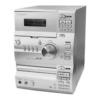
HCD-VP1 is the Amplifier, Video CD
player, Tape Deck and Tuner section
in CMT-VP1.
Dolby noise reduction manufactured under license
from Dolby Laboratories Licensing Corporation.
"DOLBY" and the double-D symbol a are trade-
marks of Dolby Laboratories Licensing Corporation.
MICROFILM
HCD-VP1
Model Name Using Similar Mechanism
CD
CD Mechanism Type
Section
Optical Pick-up Name
Model Name Using Similar Mechanism
Tape
Section
Tape Transport Mechanism Type
SPECIFICATIONS
MICRO HiFi COMPONENT SYSTEM
E Model
Chinese Model
HCD-CP1
KSL-2130CCP/K1N
KSS-213C/K1N
HCD-ED1
CMAL1Z023A
Advertisement
Table of Contents

Related Manuals for Sony HCD-VP1


Summary of Contents for Sony HCD-VP1
- Page 1 HCD-VP1 SERVICE MANUAL E Model Chinese Model HCD-VP1 is the Amplifier, Video CD player, Tape Deck and Tuner section in CMT-VP1. Dolby noise reduction manufactured under license Model Name Using Similar Mechanism HCD-CP1 from Dolby Laboratories Licensing Corporation. CD Mechanism Type KSL-2130CCP/K1N “DOLBY”...
-
Page 2: Table Of Contents
LINE WITH MARK ! ON THE SCHEMATIC DIAGRAMS AND IN THE PARTS LIST ARE CRITICAL TO SAFE OPERATION. REPLACE THESE COMPONENTS WITH SONY PARTS WHOSE PART NUMBERS APPEAR AS SHOWN IN THIS MANUAL OR IN SUPPLEMENTS PUB- LISHED BY SONY. -
Page 3: General
SECTION 1 GENERAL LOCATION OF CONTROLS • Front View 1 2 3 4 5 6 1 Tape deck 2 Liquid crystal display 3 DSG button and indicator 4 VOLUME knob 5 TAPE P button !¶ 6 TAPE 6 button !• 7 TAPE œ, p, 0, ) buttons !ª... -
Page 4: Setting The Time
This section is extracted from instruction manual. -
Page 5: Disassembly
SECTION 2 DISASSEMBLY Note: Follow the disassembly procedure in the numerical order given. COVER (UPPER) 3 cover (upper) 2 four screws (BTP3 × 8) 1 two case screws 1 two case crews TAPE MECHANISM DECK 1 flat wire (12 core) 5 tape mechanism deck 3 two screws... - Page 6 FRONT PANEL SECTION 2 flat wire (18 core) 2 flat wire (20 core) (CN802) (CN804) 1 connector 1 connector (CN812) 2 flat wire (12 core) 1 connector (CN303) 1 connector (CN809) 3 screw (KTP3 × 6) 6 connector (CN603) 5 two bosses 7 front panel section 3 screw 4 two screws...
- Page 7 CD MECHANISM DECK SECTION 3 two screws (BTP3 × 8) 2 flat wire (19 core) (CN805) 1 two connectors 1 connector (CN306) 4 CD mechanism deck section 3 two screws (BTP3 × 8) VCD BLOCK 2 three screws 3 VCD block 5 holder (VCD) 4 screw (P2 ×...
- Page 8 MECHANISM DECK ASS’Y Note: As 3 coil springs are missed easily, terat them carefully. 2 washer (2130) 3 coil spring 1 two screws (rear) (P2.6 × 10) 1 two screws (P2.6 × 10) 2 washer (2130) 2 washer (2130) 3 coil spring (rear) 3 coil spring (front)
- Page 9 • SUB CHASSIS INSTALLATION Note: Follow the assembly procedure in the numerical order given. 2 Install the drive gear with gear 5 two screws position as shown in figure. (PTPWH2.6 × 7) gear 3 screw (PTPWH2.6 × 16) front side 4 sub chassis 1 Install the control cam with gear position as shown...
-
Page 10: Service Mode
SECTION 3 SERVICE MODE [Liquid Crystal Display All Lit Check Mode] [CD Aging Mode] This mode can be used for operation check of CD section. Procedure: 1. Set to standby state. Procedure: [MD/VIDEO] 2. Press three buttons of p (TAPE), p (CD), and 1. -
Page 11: Electrical Confirmations And Adjustments
SECTION 4 ELECTRICAL CONFIRMATIONS AND ADJUSTMENTS 2. Turn the adjustment screw and check output peaks. If the peaks DECK SECTION 0 dB=0.775 V do not match for L-CH and R-CH, turn the adjustment screw Note: Confirm each contents of this section first of all. If the results are so that outputs match within 1dB of peak. - Page 12 REC Level Confirmation and Adjustment Playback level Confirmation and Adjustment Procedure: Procedure: 1. Mode: Record Mode: Playback MAIN board test tape P-4-L300 MD IN jack (PJ301) level meter (315 Hz, 0 dB) L-CH, R-CH 315 Hz, 50 mV (–23.8 dB) AF OSC blank tape –...
-
Page 13: Cd Section
RF signal waveform CD SECTION VOLT/DIV: 200 mV Notes: TIME/DIV: 500 ns 1. CD block basically constructed to operate without adjustment. There- (with the 10: 1 probe in use) fore, check each item in order given. 2. Use YEDS-18 disc (Part No.: 3-702-101-01) unless otherwise indicated. 3. -
Page 15: Diagrams
HCD-VP1 SECTION 5 DIAGRAMS 5-1. BLOCK DIAGRAM – SERVO Section – CTRL2 IC704 XTAL 16.9344MHz FILTER RF AMP, FOCUS/TRACKING ERROR AMP IC703 DETECTOR A+5V CLOCK DIGITAL SIGNAL PROCESSOR GENERATOR IC701 (1/2) DATA CD L-CH (Page 17) L-OUT DIGITAL PLL BCLK... -
Page 16: Block Diagram - Tape Section
HCD-VP1 5-2. BLOCK DIAGRAM – TAPE Section – REC-L (Page 17) DECK PROCESS, RV151 DOLBY NR AMP PLAYBACK IC352 LEVEL (L) DECK A/B PB-L PLAYBACK SELECT DOLBY NR (Page 17) EQ AMP L-CH IC351 CIRCUIT REC/PB REC/PB (Page 18) (RECORD/PLAYBACK) -
Page 17: Block Diagram - Main Section
HCD-VP1 5-3. BLOCK DIAGRAM – MAIN Section – MIC AMP IC401 J402 MIC IN RV401 MIC VOL REC-L PB-L (Page 16) (Page 16) PJ301 (1/2) INPUT SELECT SWITCH, TONE CONTROL, ELECTRICAL VOLUME MD IN IC301 LINE AMP R-CH PJ301 (2/2) -
Page 18: Block Diagram - Display/Power Supply Section
HCD-VP1 5-4. BLOCK DIAGRAM – DISPLAY/POWER SUPPLY Section – REC/PB (Page 16) BACK UP +5V SYSTEM CONTROLLER (IC801) B+ D802 RESET SIGNAL RESET 38 GENERATOR IC803 D815 LIQUID CRYSTAL DISPLAY LCD801 D814 D657 – 660 D812 B+ SWITCH (LCD BACK LIGHT) -
Page 19: Note For Printed Wiring Boards And Schematic Diagrams
HCD-VP1 5-5. NOTE FOR PRINTED WIRING BOARDS AND SCHEMATIC DIAGRAMS • Circuit Boards Location Note on Printed Wiring Boards: Note on Schematic Diagram: POWER board • X : parts extracted from the component side. • All capacitors are in µF unless otherwise noted. pF: µµF •... -
Page 20: Printed Wiring Board - Cd Board
HCD-VP1 5-6. PRINTED WIRING BOARD – CD Board – • See page 19 for Circuit Boards Location. • Semiconductor Location Ref. No. Location IC701 IC702 IC703 IC704 Q701 Q702 (Page 26) -
Page 21: Schematic Diagram - Cd Board
HCD-VP1 5-7. SCHEMATIC DIAGRAM – CD Board – • See page 31 for Waveforms. • See page 32 for IC Block Diagrams. (Page The components identified by mark ! or dotted line with mark ! are critical for safety. Replace only with part number specified. -
Page 22: Schematic Diagram - Main Board (1/4)
HCD-VP1 5-8. SCHEMATIC DIAGRAM – MAIN Board (1/4) – • See page 34 for IC Block Diagram. (Page (Page 25) (Page 23) (Page (Page 25) • Voltages and waveforms are dc with respect to ground under no-signal (detuned) conditions. no mark : FM... -
Page 23: Schematic Diagram - Main Board (2/4), Hp/Mic Board, Video Sw Board, Loading Board
HCD-VP1 5-9. SCHEMATIC DIAGRAM – MAIN Board (2/4), HP/MIC Board, VIDEO SW Board, LOADING Board – • See page 34 for IC Block Diagrams. (Page 30) (Page (Page 25) (Page 25) The components identified by mark ! or dotted line with mark ! are critical for safety. -
Page 24: Schematic Diagram - Main Board (3/4)
HCD-VP1 5-10. SCHEMATIC DIAGRAM – MAIN Board (3/4) – • See page 31 for Waveforms. (Page 22) (Page (Page 25) • Voltages and waveforms are dc with respect to ground under no-signal conditions. no mark : TAPE PLAY ) : TAPE REC... -
Page 25: Schematic Diagram - Main Board (4/4), Lcd Board
HCD-VP1 5-11. SCHEMATIC DIAGRAM – MAIN Board (4/4), LCD Board – • See page 31 for Waveforms. (Page 29) (Page 29) (Page 24) (Page 23) (Page (Page 24) (Page 22) (Page 23) (Page 22) (Page 22) -
Page 26: Printed Wiring Board - Main Board
5-12. PRINTED WIRING BOARD – MAIN Board – • See page 19 for Circuit Boards Location. HCD-VP1 (Page 27) (Page 27) (Page 28) (Page 28) (Page 20) (Page 27) (Page 27) (Page 30) (Page 27) -
Page 27: Printed Wiring Boards - Lcd Board, Hp/Mic Board, Video Sw Board, Loading Board
HCD-VP1 5-13. PRINTED WIRING BOARDS – LCD Board, HP/MIC Board, VIDEO SW Board, LOADING Board – • See page 19 for Circuit Boards Location. (Page 26) (Page 26) (Page 26) • Semiconductor Location – MAIN Board – Ref. No. Location Ref. -
Page 28: Printed Wiring Board - Control Board
HCD-VP1 5-14. PRINTED WIRING BOARD – CONTROL Board – • See page 19 for Circuit Boards Location. • Semiconductor Location Ref. No. Location D500 D501 D851 D852 D853 D854 D855 D856 D857 D858 IC802 Q500 Q501 Q852 Q853 (Page 26) -
Page 29: Schematic Diagram - Control Board
HCD-VP1 5-15. SCHEMATIC DIAGRAM – CONTROL Board – (Page 25) (Page 25) • Voltages and waveforms are dc with respect to ground under no-signal (detuned) conditions. no mark : FM... -
Page 30: Printed Wiring Board - Power Board
HCD-VP1 5-16. PRINTED WIRING BOARD – POWER Board – • See page 19 for Circuit Boards Location. 5-17. SCHEMATIC DIAGRAM – POWER Board – • Semiconductor Location Ref. No. Location D907 D908 D909 D910 D911 D912 (Page 26) D913 D914... - Page 31 • Waveforms – MAIN Board – – CD Board – 6 IC701 %∞ (RFCK) 1 Q357, 358 collector (REC mode) 1 IC703 !£ (TE) (CD play mode) 13.6 Vp-p 5.6 Vp-p 430 mVp-p 11.6 µ s 136 µ s 2 IC703 !∞ (FE) (CD play mode) 7 IC701 ^™...
- Page 32 • IC Block Diagrams – CD Board – IC701 CXD2545Q 61 – 51 DA16 EXCK DA12 LRCK WDCK SQSO PSSL SQCK MUTE SENS XRST DIRC ASYE SCLK DFSW ATSK AVDD ASYO DATA XLAT CLOK ASYI MIRR DFCT BIAS RFAC AVSS CLTV FILI LOCK...
- Page 33 IC702 BA6392FP-E2 BUFF CH1 OUT F 28 GND BUFF BUFF CH1 OUT R 27 CH4 OUT F LEVEL SHIFT CAPA IN 1 26 CH4 OUT R BUFF CH1 R IN 25 VB IN INTERFACE CH1 F IN 24 VS IN BUFF VREF IN 23 VB IN...
-
Page 34: Main Board
– MAIN Board – IC101, 201 TDA7296 THERMAL BIPOLAR SHUTDOWN TRANSCONDACTANCE INPUT STAGE MOS GAIN & SHORT – LEVEL SHIFTING OUTPUT CIRCUIT STAGE STAGE PROTECTION STANDBY/ MUTE BOOST- STRAP 14 15 IC301 TDA7439 26 25 24 23 22 21 20 19 VOLUME VOLUME TREBLE... -
Page 35: Ic Pin Function Description
5-18. IC PIN FUNCTION DESCRIPTION • MAIN BOARD IC801 CXP83120A-132Q (SYSTEM CONTROLLER, LCD DRIVER) Pin No. Pin Name Description TAPE-END Tape end detect sensor input terminal “H” input when the tape end detected — Ground terminal REMOCON Sircs remote control signal input from the remote control receiver (IC802) PLL serial data output to PLL IC on the tuner pack (at tuner function) TU-DATA/SDA C data output to the TDA7439 (IC301) (all functions) - Page 36 Pin No. Pin Name Description System reset signal input from the reset signal generator (IC803) “L”: reset RESET For several hundreds msec. after the power supply rises, “L” is input, then it changes to “H” EXTAL1 Main system clock input terminal (4.19 MHz) XTAL1 Main system clock output terminal (4.19 MHz) —...
-
Page 37: Exploded Views
SECTION 6 EXPLODED VIEWS NOTE: • -XX and -X mean standardized parts, so they • Items marked “*” are not stocked since they The components identified by mark ! or dotted line with mark may have some difference from the original are seldom required for routine service. - Page 38 (2) FRONT PANEL SECTION supplied supplied with RV801 not supplied Ref. No. Part No. Description Remark Ref. No. Part No. Description Remark X-4951-108-1 KNOB ASSY 1-418-482-11 ILLUMINATION BLOCK, LED X-4951-938-1 PANEL SUB ASSY, FRONT X-4951-937-1 LOCK (EJECT) ASSY 4-222-321-01 WINDOW (CASSETTE) 4-931-757-31 SCREW (DIA.
- Page 39 (3) CHASSIS SECTION MY, SP, HK TH, CH supplied supplied T901 KSL-2130CCP/K1N supplied supplied The components identified by mark ! or dotted line with mark ! are critical for safety. Replace only with part number specified. Ref. No. Part No. Description Remark Ref.
- Page 40 (4) CD MECHANISM DECK SECTION-1 (KSL-2130CCP/K1N) supplied supplied supplied supplied supplied M901 Ref. No. Part No. Description Remark Ref. No. Part No. Description Remark * 151 2-646-290-01 TRAY (2130) 3-319-501-51 SCREW (+PTPWH) (2.6X16) 2-625-541-02 DAMPER (S) * 162 2-646-288-01 CHASSIS (2130), SUB 2-625-279-01 SCREW (B 2.6X2.5), + * 164 1-640-523-11 LOADING BOARD...
- Page 41 (5) CD MECHANISM DECK SECTION-2 (KSL-2130CCP/K1N) not supplied not supplied M101 M102 The components identified by mark ! or dotted line with mark ! are critical for safety. Replace only with part number specified. Ref. No. Part No. Description Remark Ref.
-
Page 42: Electrical Parts List
SECTION 7 ELECTRICAL PARTS LIST NOTE: • Due to standardization, replacements in the • Items marked “*” are not stocked since they The components identified by mark ! or dotted line with mark parts list may be different from the parts speci- are seldom required for routine service. - Page 43 CONTROL Ref. No. Part No. Description Remark Ref. No. Part No. Description Remark R712 1-216-049-11 RES, CHIP 1/10W D858 8-719-075-50 LED SELS6B14C-TP5 R723 1-216-073-00 METAL CHIP 1/10W (DISC TRAY ILLUMINATION) R724 1-216-097-00 RES, CHIP 100K 1/10W R725 1-216-033-00 METAL CHIP 1/10W <...
- Page 44 CONTROL HP/MIC Ref. No. Part No. Description Remark Ref. No. Part No. Description Remark < JACK > R684 1-216-055-00 METAL CHIP 1.8K 1/10W R685 1-216-061-00 METAL CHIP 3.3K 1/10W J301 1-785-925-11 JACK (PHONES) R686 1-216-069-00 METAL CHIP 6.8K 1/10W J402 1-793-570-11 JACK (SMALL TYPE) (MIC IN) R687 1-216-073-00 METAL CHIP...
- Page 45 LOADING MAIN Ref. No. Part No. Description Remark Ref. No. Part No. Description Remark < RESISTOR > C154 1-104-666-11 ELECT 220uF C155 1-163-117-00 CERAMIC CHIP 100PF R647 1-216-181-11 RES, CHIP 1/8W R648 1-216-181-11 RES, CHIP 1/8W C156 1-130-487-00 MYLAR 0.022uF R649 1-216-181-11 RES, CHIP 1/8W...
- Page 46 MAIN Ref. No. Part No. Description Remark Ref. No. Part No. Description Remark C263 1-124-907-11 ELECT 10uF C803 1-164-004-11 CERAMIC CHIP 0.1uF C264 1-163-005-11 CERAMIC CHIP 470PF C266 1-163-007-11 CERAMIC CHIP 680PF C804 1-163-021-11 CERAMIC CHIP 0.01uF C267 1-163-003-11 CERAMIC CHIP 330PF C805 1-163-021-11 CERAMIC CHIP...
- Page 47 MAIN Ref. No. Part No. Description Remark Ref. No. Part No. Description Remark IC309 8-759-584-65 IC KA3082 Q201 8-729-920-31 TRANSISTOR DTC343TK-T-146 IC311 8-759-584-41 IC K1A7808PI Q202 8-729-920-31 TRANSISTOR DTC343TK-T-146 IC312 8-759-641-63 IC KIA7905 Q203 8-729-920-31 TRANSISTOR DTC343TK-T-146 IC350 8-759-508-69 IC BA3126N Q206 8-729-920-31 TRANSISTOR DTC343TK-T-146...
- Page 48 MAIN Ref. No. Part No. Description Remark Ref. No. Part No. Description Remark R115 1-216-073-00 METAL CHIP 1/10W R116 1-216-083-00 METAL CHIP 1/10W ! R227 1-249-389-11 CARBON 1/4W F R117 1-216-089-91 METAL CHIP 1/10W R229 1-216-073-00 METAL CHIP 1/10W R230 1-216-059-00 METAL CHIP 2.7K 1/10W...
- Page 49 MAIN Ref. No. Part No. Description Remark Ref. No. Part No. Description Remark R372 1-216-089-00 RES, CHIP 1/10W R834 1-216-049-11 RES, CHIP 1/10W R380 1-216-089-00 RES, CHIP 1/10W R835 1-216-049-11 RES, CHIP 1/10W R381 1-216-089-00 RES, CHIP 1/10W R836 1-216-049-11 RES, CHIP 1/10W R620 1-216-079-00 METAL CHIP...
- Page 50 MAIN POWER VIDEO SW Ref. No. Part No. Description Remark Ref. No. Part No. Description Remark R895 1-216-049-11 RES, CHIP 1/10W < FUSE > R896 1-216-049-11 RES, CHIP 1/10W ! F901 1-533-463-11 FUSE, GLASS TUBE (DIA. 5) (T0.63AL/250V) R897 1-216-049-11 RES, CHIP 1/10W ! F902 1-533-469-11 FUSE, GLASS TUBE (DIA.
- Page 51 Ref. No. Part No. Description Remark Ref. No. Part No. Description Remark ************** HARDWARE LIST ************** 7-685-546-14 SCREW +BTP 3X8 TYPE2 N-S 7-685-245-19 SCREW +KTP 3X6 TYPE2 NON-SLIT 7-685-246-14 SCREW +KTP 3X8 TYPE2 NON-SLIT 7-685-659-14 SCREW +BVTP 4X8 TYPE2 N-S 7-685-135-19 SCREW +P 2.6X10 TYPE2 NON-SLIT 7-621-255-32 SCREW +P 2X5 7-685-105-19 SCREW +P 2X8 TYPE2 NON-SLIT...
- Page 52 HCD-VP1 Sony Corporation 9-928-968-11 99H05082-1D Home Audio Company Printed in Japan © 1999. 8 Published by Quality Assurance Dept.
Need help?
Do you have a question about the HCD-VP1 and is the answer not in the manual?
Questions and answers