Panasonic CF-Y2 Service Manual
Cf-y2 series
Hide thumbs
Also See for CF-Y2:
- Operating instructions manual (52 pages) ,
- Reference manual (128 pages) ,
- Reference manual (213 pages)
Table of Contents
Advertisement
Quick Links
Model No. CF-Y2DWAZZ
1: Operation System
K: Microsoft
2: Area
M: Refer to above area table
1 2
®
®
Windows
XP Professional
Personal Computer
This is the Service Manual for
the following areas.
M ...for U.S.A. and Canada
© 2004 Matsushita Electric Industrial Co., Ltd. All rights reserved.
Unauthorized copying and distribution is a violation of law.
ORDER NO. CPD0406022C1
CF-Y2
Advertisement
Table of Contents
Troubleshooting

Related Manuals for Panasonic CF-Y2


Summary of Contents for Panasonic CF-Y2
- Page 1 ORDER NO. CPD0406022C1 Personal Computer CF-Y2 This is the Service Manual for the following areas. M …for U.S.A. and Canada Model No. CF-Y2DWAZZ 1: Operation System ® ® K: Microsoft Windows XP Professional 2: Area M: Refer to above area table ©...
-
Page 2: Table Of Contents
CONTENTS Page Page 1 Read Me First..............6 Disassembly & Reassembly Instruction ....1.1. Accessories ............... 6.1. Disassembly Flow Chart ........2 Specifications ..............6.2. Disassembly ............3 Names and function of Parts .......... 6.3. Reassembly ............4 Diagnosis & Repair ............7 Explanation of Hardware .......... -
Page 4: Laser Safety Information
LASER SAFETY INFORMATION For U.S.A Class 1 LASER-Product This product is certified to comply with DHHS Rules 21 CFR Subchapter J. This product complies with European Standard EN60825 (or IEC Publication 825) For all areas This equipment is classified as a class 1 level LASER product and there is no hazardous LASER radiation. Caution: (1) Use of controls or adjustments or performance of procedures other than those specified herein may result in hazardous radiation exposure. -
Page 5: Lithium Battery
LITHIUM BATTERY CAUTION Danger of explosion if battery is incorrectly replaced. Replace only with the same or equivalent type recommended by the equipment manufacture. Discard used batteries according to the manufacturer's instructions. LITHIUMBATTERIES Vorsicht! Explosionsgefahr bei unsachgemäßem Austausch der Batterie. Ersatz nur durch denselben order einen vom Hersteller empfohlenen ähnlichen Typ. - Page 9 Usage Environment Environment Place the computer on a flat stable surface. Do not place the computer upright or allow it to tip over. When the computer receives extremely strong shock after falling, the hard disk may become inoperable. In use: Temperature: 5 C to 35 C {41 F to 95 F} Humidity : 30% to 80% RH (No condensation)
- Page 10 AC adaptor ..1 Battery Pack ..1 AC Cord ....1 Model No : CF-AA1623A Model No :CF-VZSU27A Product Recovery Modem Telephone Operating Instructions DVD-ROM .... 1 Cable ....1 ....1 Windows Book ..1 ®...
-
Page 11: Accessories
2 Specification Main Specifications ® ® CPU/Cache Intel Pentium M Processor 1.3 GHz LV/1MB* On-Die Level 2 (L2) Cache Memory 256 MB* (768 MB* Max.), DDR SDRAM* Video Memory UMA (64 MB* Max.)* Hard Disk Drive Approx. 40 GB* Type 14.1 SXGA+ type (TFT) Displayed Colors* 65536/16777216 colors (1400 ×... -
Page 12: Specifications
Approx. 1.5 W when the battery pack is fully charged (or not being charged) and the computer is off. Average value. May differ depending on models. Wireless projector application software (use when making a wireless connection to Panasonic Wireless LCD Projector PT- LB10NTU.) -
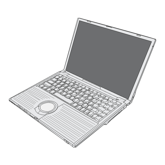
Page 13: Names And Function Of Parts
3 Names and Function of Parts Speakers To adjust the volume: Function Keys Fn + F5 / Fn + F6 For information on the key combi- Speaker on/off : Fn + F4 nations available. CAUTION Do not allow metallic objects or magnetic me- dia to come near the speakers. - Page 14 CAUTION Do not allow metallic objects or magnetic media to come near this area. External Display Port Wireless LAN DC-IN Jack DC IN 16V USB Port USB Ports CAUTION Do not allow metallic objects or magnetic media to come near this Modem area.
-
Page 15: Diagnosis & Repair
4 Diagnosis & Repair 4.1. Basic Procedures... -
Page 16: Troubleshooting
4.2. Troubleshooting... -
Page 17: List Of Error Codes
4.2.1. List of Error Codes The following is a list of the messages that BIOS can display. Most of them occur during POST. Some of them display information about a hardware device, e.g., the amount of memory installed. Others may indicate a problem with a device, such as the way it has been configured. -
Page 18: Connection Diagram
4.3. Connection Diagram Connection by Cable Connection Cable FPC ( Combo ) DFUP1368ZB Direct connection by Connectors LCD Cable DFJS893ZB Parts on Bottom Side Speaker Cable L DFJS897ZA Speaker Cable R DFJS898ZA DC Jack Cable DFJS878ZA DFJS895ZA LAN Cable DFJS896ZA Modem Cable FPC ( Pad / HDD ) DL3UP1347AAA... -
Page 19: Power-On Self Test (Boot Check)
4.4. Power-on Self Test (Boot Check) 4.4.1. Outline of POST The set has a boot check function called POST (Power-On Self Test) in it. The condition of the main body is disgnosed by checking beep sound or error code. Start ……………. Test begins automatically when power switch is set to ON. Nomal finish ……... - Page 20 The BIOS installed Default SETUP Values. If you do not want these values, enter Setup and enter your own values. If the error persists, check the system battery or contact Panasonic. 0260 System timer error The timer test failed. Requires repair of system board.
-
Page 21: Self Diagnosis Test
5.1. Outline of Self Diagnostic Tests Insert the diagnostics floppy disk Starting up the setup utility Turn on the power. When "Panasonic Press F2 to enter setup" appears on the screen, press F2. Return the setup Press " " to select [ Exit ] Press "... -
Page 22: Automatic Test
Select displayed items Error, Log, Option 5.2. Automatic Test Test execution From the menu screen shown below For Celeron models Select and press Enter for DIAG on FD 1. DIAG on FD ( CF-Y2 ) 2. LAN test 3. SD I/F test 4. Modem test 5. -
Page 24: Test Selection
5.4. Test Selection Starting up the input menu 1. From the menu screen shown below, choose Quit and press Enter. 1. DIAG on FD (CF-Y2) 2. LAN test 3. SD I/F test 4. Modem test 5. Wireless LAN test (Wireless LAN Model only) Q. -
Page 25: Error Messages And Troubleshooting
5.5. Error Messages and Troubleshooting The table below explains the parts that may be faulty or damaged should an error message occur while performing the various test items of the self diagnostics program. Test classification Screen display test items Contents Possible damaged or faulty part A20 GATE TEST Address 20 line... -
Page 26: Disassembly & Reassembly Instruction
6 Disassembly & Reassembly Instructions 6.1. Disassembly Flowchart The chart below shows the various parts which should be removed in order to remove the parts that are to be replaced. Parts can be replaced efficiently by following the disassembly steps in the chart. -
Page 27: Disassembly
2. Operate the Open Button of the LCD Unit, and open the 6.2. Disassembly LCD Block to an angle of 90 degrees or more. 6.2.1. Preparations Release the four hooks of the LCD Unit and the two hooks, one at the left and one at the right, by inserting a regular Before disassembly, be sure to perform the following steps. - Page 28 3. Operate the Open Button of the LCD Unit, and open the 7. Remove the nine Screws (F) of the Top Cabinet Ass’y. LCD Block to an angle of 90 degrees or more. Screw (F): DXQT2+G6FZL 4. Remove the Screws (E) and the six Hooks, and then remove the Side Cover (R).
-
Page 29: Removing The Hdd
6.2.4. Removing the LCD Block 6.2.6. Removing the MDC Modem Board Preparation: Make sure that the steps in sections 6.2.1 to Preparation: Make sure that the steps in sections 6.2.1 to 6.2.3 have been taken first. 6.2.5 have been taken first. (The entire unit is now standing upright with the LCD 1. - Page 30 7. Remove the Screw (Q), and remove the Drive/Open Board. 6.2.8. Removing the Latch Knob Screw (Q): DXHM0056ZA Preparation: Make sure that the steps in sections 6.2.1 to 6.2.5 have been taken first. 1. Remove the LCD Knob Spring. 2. Remove the Screw (X), and remove the Latch Knob from the Top Cabinet Ass’y.
-
Page 31: Touch Pad
9. Peel off the tape that secures the Wireless LAN Module. 2. Release the Pad Button Hooks, and remove the Pad Button from the Top Cabinet Ass’y. 10. Release the Module Locks, and remove the Wireless LAN Module. 3. Remove the Pad/HDD FPC from the Touch Pad Connector. 6.2.11. - Page 32 5. Remove Screw (U), and disconnect the Pad/HDD FPC from 6.2.13. Removing the Speaker (L), (R) the Top Cabinet Ass’y. Preparation: Make sure that the steps in sections 6.2.1 to Screw (U): DXHM0056ZA 6.2.4 and section 6.2.10 have been taken first. 1.
-
Page 33: Removing The Inverter Board
6.2.15. Removing the LCD Unit/LCD Cable 2. Remove the Screw (Z) from the Hinge (L) and the Screw (Z) from Hinge (R). Preparation: Make sure that the steps in sections 6.2.1 to Screw (Z): DXHM0002ZA 6.2.4 and section 6.2.14 have been taken first. 3. -
Page 34: Reassembly
6.3. Reassembly 6.3.1. Screw Tightening Sequence for the Units After servicing, tighten the screws in the following sequence. 1. Tightening the screws of the LCD Unit. 1-1.Tighten DXYN3+J5FNL(J). No.1, No.2 1-2.Tighten XTB26+10GFN(H). No.3, No.4 2. Tightening the screws of the Bottom Cabinet Ass’y After holding down area (A): 2-1.Tighten DXHM0039ZA(B). - Page 35 6.3.2. Routing the LCD Cable 6.3.4. Reassembling the Keyboard * When making repairs, be absolutely sure to re-apply the heat- releasing grease (using an amount equivalent to the size of a pea). * Anchor the Keyboard tightly using the four hooks of the LCD. 6.3.5.
-
Page 38: Main Unit Extended View
8 Main Unit Extended View 8.1. Display Section CF-Y2DWAZZKM... -
Page 39: Cabinet Section
8.2. Cabinet Section 8.2.1 Top side K101 K100 E12-1 K51-2 K51-1 K51-4 K51-3 K51-5 K51-6 E13-1 CN911 SW911 SW910 JK911 K102 JK910 SW920 CN24 CF-Y2DWAZZKM... -
Page 40: Bottom Side
8.2.2. Bottom side K110 K110 K50-1 K110 K50-1 K50-1 K50-1 K50-1 K111 K105 K109 K107 CF-Y2DWAZZKM... -
Page 41: Replacement Parts List
9 Replacement Parts List Note: Important Safety Notice Components identified by mark have special characteristics important for safety. When replacing any of these components, use only manufacturer's specified parts. CF-Y2DWAZZKM REF.NO.and AREA PART NO. DESCRIPTION Q'TY Main Block Unit CR2032/S5Y LITHIUM BATTERY DFUP1368ZB FPC,DRIVE... - Page 42 DFBD0176ZA-0 KNOB,DRIVE DFBH1173ZA HINGE-L DFBH1174ZA HINGE-R DFDF3152ZA SHAFT, DISK COVER-1 DFGX0381ZA-0 RING, PAD K 10 DFGX0403ZB-0 COVER, HINGE-L K 11 DFGX0404ZB-0 COVER, HINGE-R K 12 DFGX0406ZA-0 COVER, RJ DUST K 13 DFHE0463ZA SHEET,EMI A K 14 DFHE0472ZA SHEET, EMI PAD FPC K 15 DFHE0555ZA GASKET 1...
- Page 43 K 62 DFMX1095ZA SHEET, VGA K 63 DFMX1120ZA CASE, INVERTER K 64 DFMY3151ZA THERMAL PLATE K 65 DFMY3171ZA MEMORY SHEET K 66 DFQT9675ZA LABEL, ENERGY STAR K 67 DFQT9775ZA LABEL, WIN LOGO K 68 DFQT9867ZA LABEL, CENTRINO K 69 DFUD0037ZA SPRING, DISK KNOB K 70 DFUN0073ZA...
- Page 44 Replacement Parts List Note: Important Safety Notice Components identified by mark have special characteristics important for safety. When replacing any of these components use only manufacturer's specified parts. CF-Y2DWAZZKM REF. NO and AREA PART NO. DESCRIPTION Q'TY MAIN PCB C 1 486 487 488 EEFUD0D271XR CAPACITOR, 2V, 270µF C 123 481 500 520...
- Page 45 C 525 F1H1E472A050 CAPACITOR, 25V, 4700pF C 54 F1G1H222A450 CAPACITOR, 50V, 2200pF C 559 560 DCUI1C106HDB CAPACITOR, 16V, 10µF C 56 60 61 67 68 69 199 202 529 F1G1A104A014 CAPACITOR, 10V, 0.1µF C 57 58 59 88 89 90 93 94 120 134 ECJ0EF1C104Z CAPACITOR, 16V, 0.1µF 137 139 143 148 149 150 152 153 157...
- Page 46 D 4 5 11 53 68 MA2J72900L DIODE D 41 DED03P2JT1-D DIODE D 45 54 B0JCCE000008 DIODE D 46 DEDRB081L20 DIODE D 6 63 MA3J741E0L DIODE D 62 DEDF1J3ETP DIODE D 64 65 66 67 EZJZ0V500AA VARISTOR F 1 2 K5H2021A0003 FUSE, 24V, 2A IC 1...
- Page 47 PS 1 K5J1BB000001 POLY SW B1HBCFA00006 TRANSISTOR Q 10 15 20 21 22 27 66 67 91 117 B1DHDC000021 TRANSISTOR Q 14 17 18 24 58 63 64 65 69 103 107 XP0421300L TRANSISTOR 108 110 Q 16 2SB0709A0L TRANSISTOR Q 3 5 9 45 46 56 59 62 68 81 87 100 UNR9213J0L TRANSISTOR...
- Page 48 R 271 272 273 ERJ2GEJ333X RESISTOR, 1/16W, 33KΩ R 276 ERJ2GEJ471X RESISTOR, 1/16W, 470Ω R 30 215 352 356 357 ERJ2GEJ562X RESISTOR, 1/16W, 5.6KΩ R 323 ERJ2RKF3901X RESISTOR, 1/16W, 3.9KΩ R 326 351 353 512 ERJ2RHD103X RESISTOR, 1/16W, 10KΩ R 344 347 ERJ2RHD104X RESISTOR, 1/16W, 100KΩ...
- Page 49 ERJ2RKF3002X RESISTOR, 1/16W, 30KΩ R 583 R 598 ERJ2RKF47R5X RESISTOR, 1/16W, 47.5Ω R 6 18 19 ERJ2RKF54R9X RESISTOR, 1/16W, 54.9Ω R 61 ERJ2RKF40R2X RESISTOR, 1/16W, 40.2Ω R 63 126 127 137 138 139 144 146 ERJ2GEJ103X RESISTOR, 1/16W, 10KΩ 150 168 169 170 192 199 210 250 257 260 262 263 264 283 327 331 359 370 386 441 448 456 461 462 469 480 486 487 544 548 555 562 563 564 565 566...
- Page 50 PAD /HDD FPC SW 900 901 EVQPLDA15 CN 900 K1KAA0A00121 CONNECTOR CN 902 K1KB30A00131 CONNECTOR CN 901 DFJS502ZA044 CONNECTOR...
- Page 51 CF-Y2 Printed Circuit Board Main Board <Top Side>...
- Page 52 CF-Y2 Printed Circuit Board Main Board <Bottom Side>...
- Page 53 CF-Y2 Schematic Diagrams Main 1 Dothan HostBus VC18 VC15 003:F6 GTLA0_HA#[3-16] GTLD3_HD#[48-63] BaniasLV1.3G uFCBGA 003:I1 DL3UP1345FAA/GAA/HAA 12.7-139mm GTLA0_HA#[3] GTLD3_HD#[63] AF26 D#[63] 1608 1608 A#[3] 12.7-165mm Banias1.3G LV GTLA0_HA#[4] BaniasLV1.3G uFCBGA GTLD3_HD#[62] AF22 D#[62] A#[4] RJ80535LC0313MSL6NA GTLA0_HA#[5] D6 VCC_CORE GTLD3_HD#[61] AF25 D#[61]...
- Page 54 Main 2 Dothan Power BaniasLV1.3G uFCBGA VCTREF VCCP THERMDA AC10 THERMDA 002:E9 THERMDC 002:E9 THERMDC CPU_THERMTRIP# 002:G4 THERMTRIP# CPU_PROCHOT# B17 PROCHOT# 002:G6 AB26 CPU_DPSLP# CPU_FERR# ICH_FERR# AB23 003:I8;010:D4 DPSLP# 001:G9 010:D4 CPU_DPWR# AB21 DPWR# 003:I7 PSI# AB19 PSI# 029:A5 AB17 COMP[0] AB15 AB2 COMP[2]...
- Page 55 Main 3 MontaraGM+ DDR, HostBus GTLD0_HD#[0-15] GTLA0_HA#[3-16] 001:E6 SD_DQ[0-63] MONTARA-GM+ 001:H1 SD_MA[0-12] MONTARA-GM+ 8:F6,005:G2;007:B6;008:B6,005:G2;007:F2;008:B8,005:G2;007:E6;008:B6,005:G2;007:B6;008:B6 GTLD0_HD#[0] GTLA0_HA#[3] K22 HD0# HA3# SD_MA[0] SD_DQ[0] AC18 SMA0 SDQ0 GTLD0_HD#[1] GTLA0_HA#[4] H27 HD1# HA4# SD_MA[1] SD_DQ[1] AD14 SMA1 VCCP SDQ1 GTLD0_HD#[2] GTLA0_HA#[5] K25 HD2# HA5# SD_MA[2] SD_DQ[2] AD13 SMA2...
- Page 56 Main 4 MontaraGM+ Power, DVO MONTARA-GM+ AA29 VSS VCCADPLLA VCCADPLLB VCMCH VCMCH W29 VSS MONTARA-GM+ U29 VSS MONTARA-GM+ 0.1u V29 VTTHF N29 VSS VCCAHPLL R3 DVOBD0 HUB_HL00 0.1u M29 VTTHF L29 VSS VCCAGPLL 010:D5 R5 DVOBD1 HUB_HL01 0.1u H29 VTTHF J29 VSS VCCADPLLA 010:D5...
- Page 57 Main 5 DDR Dump R data signals SD_DQ[0-63] SD_RDQ[0-63] ;007:B1;008:G8,003:E1;007:B1;008:G8,003:E1;007:B1;008:G7 006:A1 command signals SD_DQ[0] SD_RDQ[0] SD_DQ[1] SD_RDQ[1] SD_DQ[2] SD_RDQ[2] SD_MA[0-12] SD_DQ[3] SD_RDQ[3] SD_RMA[0-12] SD_DQ[4] SD_RDQ[4] 006:A1 SD_DQ[5] SD_RDQ[5] SD_DQ[6] SD_RDQ[6] SD_DQ[7] SD_RDQ[7] RA12 10 SD_DQ[8] SD_RDQ[8] SD_MA[0] SD_RMA[0] SD_DQ[9] SD_RDQ[9] SD_MA[3] SD_RMA[3] SD_DQ[10]...
- Page 58 Main 6 On Board Memory Bank 0 / 1 SD_RDQ[0-63] 005:D1 BANK 0/1 (ON BOARD) SD_RMA[0-12] 005:J2 K4H561638D-GCB3 K4H561638D-GCB3 K4H561638D-GCB3 K4H561638D-GCB3 IC10 IC12 256Mbit PKG size = 8x14mm SD_RBA0 SD_RDQ[15] SD_RDQ[31] SD_RDQ[47] SD_RDQ[63] 512Mbit PKG size = 10x12mm SD_RBA0 SD_RBA0 SD_RBA0 I3;006:B7;006:C1;006:C7;006:E1;006:E7;006:G1;006:G7 SD_RBA1...
- Page 59 Main 7 Micro - DIMM Bank 2 / 3 MicroDDR 1-1746705-1 BANK 2/3 (Micro-DIMM) SD_DQ[0-63] A1;008:G8,003:E1;005:A1;008:G8,003:E1;005:A1;008:G8,003:E1;005:A1;008:G7 MicroDDR MicroDDR VB25 MEMREF MEMREF VB25 VB25 1-1746705-1 VB25 1-1746705-1 0.1u C149 VREF VREF SD_MA[10] SD_BA1 87 A10/AP C150 003:B1;005:G2;008:B8 003:C3;005:G3;008:F6 0.1u 89 VDD SD_DQ[0] SD_DQ[4] SD_BA0...
- Page 60 Main 8 DDR Term VC125 VC125 RA13 RA45 SD_DQS[0] 003:E8;005:A10;007:B3 SD_DQS[1] 003:E8;005:A10;007:B3 SD_DQ[5] C162 SD_CKE0 003:E1;005:A1;007:B1 SD_DQ[4] 003:B8;006:A3;006:C3;006:E3;006:G3 SD_CKE1 003:E1;005:A1;007:B1 0.1u 003:B8;006:A9;006:C9;006:E9;006:G9 SD_DQ[0] 003:E1;005:A1;007:B1 SD_DQ[1] 003:E1;005:A1;007:B1 RA20 SD_DQ[2] 003:E1;005:A1;007:B1 SD_DQ[3] 003:E1;005:A1;007:B1 SD_DM[0] 003:B4;005:A9;007:E3 SD_DQ[6] RA14 C169 003:E1;005:A1;007:B1 SD_DQ[16] SD_DM[1] 003:E1;005:A1;007:B1 003:B4;005:A9;007:E3 SD_DQ[17] 0.1u...
- Page 61 Main 9 Clock Generator N2012ZP600T25 C761 6.3V ADDR:D2h 2125 0.01u C765 VC3PLL VC3PLL CK-408 IC17 1 VDD N2012ZP600T25 8 VDD C179 C181 C182 C183 C184 C187 14 VDD 0.1u 0.01u 0.1u 0.01u 0.1u 0.01u 19 VDD ITP_BCLK0 32 VDD R112 AVSS TP97 001:A8...
- Page 62 Main 10 ICH4 - M RA27 ICH4-M SMBCLK R140 PME# R150 SMBDATA AGPBUSY# R2 AGPBUSY# ICH_GPIO1 GPIO7 R126 SYSRESET# R137 004:G9;011:F6 SMLINK0 R146 Y5 LANRST# ECSMI# GPIO8 ICH_GPIO0 022:D8;022:H2 R127 SMLINK1 ECBTLW# AB2 BATLOW# ECSCI# GPIO12 022:D9;022:H2 022:D7;022:H2 VCCP PCIRST# T3 GPO21/C3STAT R138 R130...
- Page 63 Main 11 ICH4 - M Power ICH4-M ICH4-M RA30 FRAME# DDR TYPE V8 VCCSUS3_3 A1 VSS 010:B9;015:B6;017:D8;018:E7 VCC3_3 IRDY# V9 VCCSUS3_3 A16 VSS RAM_ID1 RAM_ID0 VCC3_3 010:B10;015:B6;017:D8;018:B7 SizexQ’ty/Total TRDY# F18 VCCSUS3_3 A18 VSS 010:B11;015:B6;017:D8;018:E7 256Mx8/256MB Def. VCC3_3 STOP# 256Mx4/128MB E11 VCCSUS3_3 A20 VSS 010:B11;015:B7;017:D8;018:E7 VCC3_3...
- Page 64 Main 12 Combo Drive DVD5V RSTDRV 010:F11;024:D2 Q108 XP0421300L R182 CDRST 010:F9 Q108 XP0421300L SDD[0-15] 010:H5 DRIVE_CN Top Contact CDAUDIOL CDAUDIOR 019:F7 019:F7 CDAUDIOG 019:F9 SDD[8] SDD[7] SDD[9] SDD[6] SDD[10] SDD[5] SDD[11] SDD[4] SDD[12] SDD[3] SDD[13] SDD[2] SDD[14] SDD[1] SDD[15] SDD[0] SDDREQ 010:I8...
- Page 65 Main 13 USB C245 0.1u IC22 R569 R566 LM3526MX-H USBPW1 1 ENA OUTA 013:E4 USBOC1# 2 FLGA 010:F7 USBOC0# 3 FLGB 010:F7 USBEN0 USBPW0 4 ENB OUTB 013:E7 022:F3 SOP8 N2012ZP600T25 USBPW1 013:G3 SP-CAP C724 6.3V C247 470p 150u USB1 87520-4010B EEFUE0J151R ACM2012-900-2P...
- Page 66 Main 14 CRT, LCD I / F FDW254P R185 100K C248 2125 0.01u KAB2402202NA31 Pch-MOSFET LCD CN FPVCC TSSOP8 R192 UNR9213J0L 004:I8 FAIRCHILD C252 0.1u R186 FP_ID 010:E9;011:H4 100K LVYAD0- 004:I5 ECLID# LID# LVYAD0+ ICH4-M C782 004:I5 100p LVYAD1- 004:I5 LVYAD1+ BLPWM 004:I6...
- Page 67 Main 15 Card-Bus Controller IC26 ACADR[0-25] IC25 SN74AHC1G08DCKR C763 AD[0-31] IC25 VCC_SD 0.1u R5C576A-CSP277 BCADR[0-10] R5C576A-CSP277 ACADR[25] C19 A_A25 B_A25 AD[31] AD31 ACADR[24] F16 A_A24 B_A24 AD[30] AD30 ACADR[23] G15 A_A23 B_A23 AD[29] SDC_DAT3 SDC_DAT3 IC26 AD29 ACADR[22] 024:E6 SUSCLK E18 A_A22 B_A22 AD[28]...
- Page 68 Main 16 Card Slot BCDATA[0-15] ACADR[0-25] 015:J5 015:G1 BCADR[0-10] PCMCIA ACDATA[0-15] 015:J1 CF SUB CN29 Solder Side View CN12 BCD1# ACDATA[3] ACD1# 015:I9;016:E10 015:H9;016:E10 BCDATA[3] ACDATA[4] ACDATA[11] BCDATA[11] ACDATA[5] ACDATA[12] BCDATA[4] ACDATA[6] ACDATA[13] BCDATA[12] ACDATA[7] BCDATA[5] ACDATA[14] ACE1# 015:H7 BCDATA[13] ACDATA[15] ACADR[10] BCDATA[6]...
- Page 69 Main 17 LAN VLAN TPC6104 Pch-MOSFET SOT6 R209 C293 IC18 LAN CN 100K TLA-6T211A 010:B3;015:B1;018:B2 Ethernet IC C287 0.01u AD[0-31] CN14 R211 RTL8139DL 1 TD+ 330K AD[31] 86 AD31 3 TDC TXD+ VLANON XP0421300L AD[30] 87 AD30 2 TD- TXD- 022:F6 AD[29] 89 AD29...
- Page 70 Main 18 mini PCI V5MINI V3MINI VA3MINI TPC6104 C309 C310 0.1u V3MINI 2125 XP0421300L SLP_S3# Pch-MOSFET 009:D5;010:F2;017:A4;018:G6;018:G8;022:F4;024:H2;025:D5;028:A5;028:A7;028:B11;028:D5;031:C4 SOT6 R241 C311 100K AD[0-31] 0.01u 2125 C312 010:B3;015:B1;017:D3 R244 100K VA3MINI MINIVA3ON MINI-PCI 022:F5 XP0421300L CN15 1612755-1 1 TIP RING R533 USBP2+ R531 3 <LAN>...
- Page 71 Main 19 AC97 Codec JP10 1608JP SNDGND IC33 R1114N331A-TR-FA 5 OUT 4 NC VCODEC C331 RICOH IC32 2125 STAC9751TGCC1 C335 6.3V 1 DVdd1 AVdd1 10V 1608 9 DVdd2 AVdd2 2125 C318 C320 SNDGND C317 6.3V 0.01u 0.1u 4 DVss1 AVss1 7 DVss2 AVss2 SNDGND...
- Page 72 Main 20 Audio AMP. C574 6.3V SP_L VC5AMP 2125 CN27 12/23:R261 47K 100K C578 R546 10 C358 6.3V IC36 2125 N2012ZP600T25 TPA0122PWPR C573 1608 0.1u 100K SM02B-SRSS-TB BEEPSP C359 HPROUT R261 SNDGND 14 PC-BEEP 6.3V 020:F6 024:G7 2125 C571 C572 0.1u 22 SHOTDOWN# SP-CAP...
- Page 73 Main 21 FWH IC60 Pm49FL004T-33VC FGPI4(A10) RFU(DQ7) FGPI3(A9) RFU(DQ6) FGPI2(A8) RFU(DQ5) FGPI1(A7) RFU(DQ4) LAD3 FGPI0(A6) AD3(DQ3) 010:F5;022:D10 FWHWP# LAD2 022:F5 WP#(A5) AD2(DQ2) 010:F5;022:D10 FWHTBL# LAD1 022:F5 AD1(DQ1) TBL#(A4) 010:F5;022:D10 LAD0 ID3(A3) AD0(DQ0) 010:F5;022:D10 ID2(A2) ID1(A1) ID0(A0) PCIRST# RST#(RST#) CLK_FWHPCI 009:H6 CLK(R/C#) LFRAME# 010:F6;022:D10...
- Page 74 Main 22 KBC & EC KBC&EC IC41 SUSCLK R328 17 P87/XCIN P83/TB1IN 004:E7;010:F3;015:E2 18 P86/XCOUT EXTTS# P82/TB0IN TP58 004:I10 HSTOP# P81/TA4IN 018:E9 BLBEEP 38 P67//TXD10 MOD_ON P80/ICCK RA38 020:C7;022:A4 018:B4 ECPWRSW# FRXD 39 P66//RXD10 010:F2;022:F8 022:A3 ECLID# FSCLK 40 P65/CLK10 P57/CLKOUT/KI07 KB_IN[7] 010:D3;022:D7...
- Page 75 Main 23 Keyboad CN KB_OUT[1-16] 022:F9,022:F9,022:F9,022:F8,022:F8,022:F8,022:F8,022:F8,022:D7,022:D6,022:D6,022:D6,022:D6,022:D6,022:D6,022:D6 KB CN1 CN35 KB_OUT[16] KB_OUT[15] KB_OUT[14] KB_OUT[13] KB_OUT[12] KB_OUT[11] KB_OUT[10] KB_OUT[9] KB_OUT[8] KB_OUT[7] KB_OUT[6] KB_OUT[5] KB_OUT[4] KB_OUT[3] KB_OUT[2] KB_OUT[1] SFW16S-6STME1 RA39 KB CN2 KB_IN[0-7] 022:F2,022:F2,022:F2,022:F2,022:F2,022:F2,022:F2,022:F2 CN34 KB_IN[7] KB_IN[6] KB_IN[5] KB_IN[4] KB_IN[3] KB_IN[2] KB_IN[1] KB_IN[0] JP Open US - JP Open...
- Page 76 Main 24 Front PCB CN VCHDM V3MDC TPC6104 R178 XP0421300L SLP_S3# 009:D5;010:F2;017:A4;018:G6;018:G8;018:H2;022:F4;025:D5;028:A5;028:A7;028:B11;028:D5;031:C4 C760 Pch-MOSFET 6.3V SOT6 R298 100K 2125 C375 0.01u Front CN RSTDRV R301 010:F11;012:C2 CN36 100K VMODEMON UNR9213J0L 022:F6 XP0421300L PDD[7] PDD[8] 010:H3 010:H3 PDD[6] PDD[9] SUSLED# UNR9113J0L 010:H3 010:H3 022:F6...
- Page 77 Main 25 Reset tD=0.69x6.5x10 xC R343 Target 210ms IC43 R3112Q251C IC61 1 VCC VOUT IC46 C425 VCRST# 007:H9;010:C2;010:F2;017:C9;022:D4;028:B11 2 GND SN74AHC1G08DCKR SN74AHC1G08DCKR RICOH C433 C428 1000p 0.047u SLP_S3# 009:D5;010:F2;017:A4;018:G6;018:G8;018:H2;022:F4;024:H2;028:A5;028:A7;028:B11;028:D5;031:C4 DBRESET# IC61 IC46 001:A10 C434 SN74AHC1G08DCKR SN74AHC1G08DCKR 0.1u Target 45ms IC44 R3112Q251C 1 VCC VBRST#...
- Page 78 Main 26 DCin BATTin FDS4435A DC-IN ACIN DCIN&BATT CN23 S2B-PH-SM3-TB F1J3ETP 0.33 R367 C445 2125 1608 R364 0.1u 2125 Pch-MOSFET 0.27 R350 1/4W 100K C435 R368 SOP8(1.75mH) 5.6K 0.47 2125 FAIRCHILD 2125 1608 R354 R359 AC15 0.27 R365 R369 R357 100K C439 5.6K...
- Page 79 Main 28 VB3 VC3 VB5 VC5 OVP TPC6104 Pch-MOSFET R394 SOT6 2.2M C468 0.047u 100K R396 SLP_S4# XP0421300L TPC6104 FDW254P ACIN BATVOL BATVOL ACIN SP-CAP 6.3V Pch-MOSFET C466 MA2S11100L R393 SOT6 C469 R388 Pch-MOSFET 0.047u MA2S11100L EEFCD0J470R 560K C464 TSSOP8 MA2S11100L 0.047u MA2S11100L...
- Page 80 Main 29 VCPUCORE High Frequency mode=>1.052V Low Frequency mode =>0.956V Deep Sleep mode VCPUCOREx97.4% Deeper Sleeper mode at HFM =>0.748V Deeper Sleeper mode at LFM =>0.748V R430 2003.7.23 R443 5m 1608 Max.12.0A C474 1u B 1608 SGND 1SS357(TPH3F) PGOOD 1.7m MCH_OK @compC @compC...
- Page 81 Main 30 VCCP VCMCH DCIN&BATT R454 1608 1608 C495 0.1u RB717FT106 INTVCC 2SK3019TL VRON# 2SK3019TL VRON# 2125 C500 4.7u 1608 1608 C502 C492 0.1u 0.1u Imax=50mV/Rsense PGND DCIN&BATT Imax=50mV/Rsense FDS6912A VCMCH 1 S1 VCCP 1.05V 2 G1 Rdson=13m R446 25 SW1 3 S2 R472 26 TG1...
- Page 82 Main 31 VB25(DDR) VC15 DCIN&BATT R478 1608 1608 C515 DCIN&BATT 0.1u DCIN&BATT R492 RB717FT106 100K R475 100K INTVCC1 2SK3019TL 2SK3019TL SLP_S4# C520 2125 010:F3;016:E5;022:F4;028:B9;028:D3 SLP_S3# 009:D5;010:F2;017:A4;018:G6;018:G8;018:H2;022:F4;024:H2;025:D5;028:A5;028:A7;028:B11;028:D5 4.7u UNR9213J0L UNR9213J0L 1608 1608 DCIN&BATT C522 C512 0.1u 0.1u Imax=50mV/Rsense PGND Imax=50mV/Rsense VB25=2.5V 125mV@ 4.2A SI6410DQ VB25...
- Page 83 Main 32 VC125(DDR) GMCH(VC3 VC15) 2003.9.3 C531 NU C533 NU VC125 VC125=1.25V 62.5mV@1.5A IC55 SP-CAP VB25 6.3V LP2996MX 1 GND C533 C534 150u 2 SD PVIN 2125 EEFUD0G151R 3 VSNS AVIN 4 VREF VDDQ 2125 6.3V 6.3V C531 C530 C529 0.1u MEMREF 2125...
- Page 84 Main 33 VA15 VC18 VA15 IC58 R1114N151A-TR-FA 1 Vin 3 CE# 2 GND 6.3V C541 2125 RICOH C543 1608 VC18 IC57 R1114N181A-TR-FA 1 Vin 3 CE# 2 GND RICOH 6.3V C540 2125 C542 1608...
- Page 85 Main 34 Charge ACIN R514 DCIN&BATT C557 C558 R508 R516 C551 026:H3 3225 3225 1 DCIN IINP SENSE+ 2125 C544 SOP8 2 LDO CSSP FAIRCHILD FDS6690A C552 C545 @partN 2125 R517 C549 3 CLS CSSN 2125 026:H3 1608 PGND 1608 SENSE- 4 REF 0.22...
Need help?
Do you have a question about the CF-Y2 and is the answer not in the manual?
Questions and answers