Table of Contents
Advertisement
Quick Links
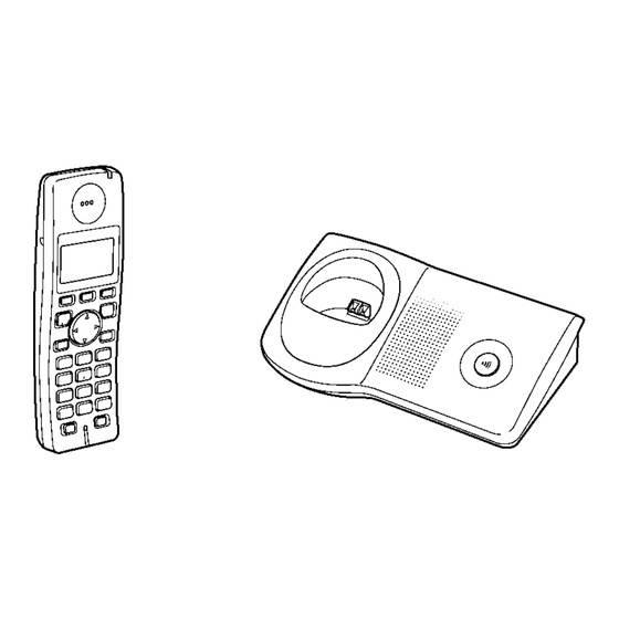
Telephone Equipment
KX-TG7100FXS
KX-TG7100FXT
KX-TG7102FXS
KX-TGA711FXS
KX-TGA711FXT
Digital Cordless Phone
Silver Version
Titanium Black Version
(for Central Europe)
© 2006 Panasonic Communications Co., Ltd. All
rights reserved. Unauthorized copying and distribu-
tion is a violation of law.
ORDER NO. KM40605064CE
Advertisement
Table of Contents
Troubleshooting

Related Manuals for Panasonic KX-TG7100FXS


Summary of Contents for Panasonic KX-TG7100FXS
- Page 1 ORDER NO. KM40605064CE Telephone Equipment KX-TG7100FXS KX-TG7100FXT KX-TG7102FXS KX-TGA711FXS KX-TGA711FXT Digital Cordless Phone Silver Version Titanium Black Version (for Central Europe) © 2006 Panasonic Communications Co., Ltd. All rights reserved. Unauthorized copying and distribu- tion is a violation of law.
- Page 2 KX-TG7100FXS/KX-TG7100FXT/KX-TG7102FXS/KX-TGA711FXS/KX-TGA711FXT...
-
Page 3: Table Of Contents
KX-TG7100FXS/KX-TG7100FXT/KX-TG7102FXS/KX-TGA711FXS/KX-TGA711FXT TABLE OF CONTENTS PAGE PAGE 1 Safety Precaution ------------------------------------------------ 4 14.3. Terminal Guide of the ICs, Transistors and 1.1. For Service Technicians --------------------------------- 4 Diodes ------------------------------------------------------ 72 2 Warning -------------------------------------------------------------- 4 15 Exploded View and Replacement Parts List ----------- 73 2.1. -
Page 4: Safety Precaution
KX-TG7100FXS/KX-TG7100FXT/KX-TG7102FXS/KX-TGA711FXS/KX-TGA711FXT 1 Safety Precaution 1.1. For Service Technicians ICs and LSIs are vulnerable to static electricity. When repairing, the following precautions will help prevent recurring malfunctions. 1. Cover the plastic parts boxes with aluminum foil and ground them. 2. Ground the soldering irons. -
Page 5: How To Recognize That Pb Free Solder Is Used
KX-TG7100FXS/KX-TG7100FXT/KX-TG7102FXS/KX-TGA711FXS/KX-TGA711FXT 2.2.1. Suggested PbF Solder There are several types of PbF solder available commercially. While this product is manufactured using Tin, Silver, and Copper (Sn+Ag+Cu), you can also use Tin and Copper (Sn+Cu) or Tin, Zinc, and Bismuth (Sn+Zn+Bi). Please check the manufac- turer’s specific instructions for the melting points of their products and any precautions for using their product with other materi-... -
Page 6: Specifications
KX-TG7100FXS/KX-TG7100FXT/KX-TG7102FXS/KX-TGA711FXS/KX-TGA711FXT 3 Specifications Note: • Specifications are subject to change. Connections: • The unit will not work during a power failure. We recommend you connect a standard telephone on the same line for power pro- tection. Note for Service: • Operation range: Up to 300 m outdoors, Up to 50 m indoors... -
Page 7: Technical Descriptions
KX-TG7100FXS/KX-TG7100FXT/KX-TG7102FXS/KX-TGA711FXS/KX-TGA711FXT 4 Technical Descriptions 4.1. Block Diagram (Base Unit) -
Page 8: Circuit Operation (Base Unit)
KX-TG7100FXS/KX-TG7100FXT/KX-TG7102FXS/KX-TGA711FXS/KX-TGA711FXT 4.2. Circuit Operation (Base Unit) 4.2.1. Outline Base Unit consists of the following ICs as shown in Block Diagram (Base Unit) (P.7). • DECT BBIC (Base Band IC): IC7 - Handling all the audio, signal and data processing needed in a DECT base unit... -
Page 9: Power Supply Circuit
KX-TG7100FXS/KX-TG7100FXT/KX-TG7102FXS/KX-TGA711FXS/KX-TGA711FXT 4.2.2. Power Supply Circuit The power is supplied to the DECT BBIC, RF Module, EEPROM and Charge Contact from AC Adaptor (+6.5 V) as shown in Fig.101. The power supply is as follows; • DECT BBIC (IC7): CN2 (+6.5 V) → IC1 → Q9 → IC7 CN2 (+6.5 V) →... -
Page 10: Pulse Dialing
KX-TG7100FXS/KX-TG7100FXT/KX-TG7102FXS/KX-TGA711FXS/KX-TGA711FXT 4.2.4. Transmitter/Receiver • Audio Circuits and DTMF tone signal circuits. Base Unit and Handset mainly consist of RF Module and DECT BBIC. Base Unit and Handset transmit/receive voice signal and data signal through the antenna on carrier frequency. Signal Path: *Refer to Signal Route (P.13). -
Page 11: Block Diagram (Handset)
KX-TG7100FXS/KX-TG7100FXT/KX-TG7102FXS/KX-TGA711FXS/KX-TGA711FXT 4.3. Block Diagram (Handset) SPEAKER RXDA Speech Burst Decoding Decoding TXDA RECEIVER Speech Burst Module Encoding Encoding RSSI ADPCM SYDA Codec SYEN Analog Interface Filter SYCL Front CHARGE(+) CHARGE XTAL CHARGE CHARGE CIRCUIT CONTACTS CHARGE DETECT Q4,Q5,Q9 10.368 CHARGE(-) -
Page 12: Charge Circuit
KX-TG7100FXS/KX-TG7100FXT/KX-TG7102FXS/KX-TGA711FXS/KX-TGA711FXT 4.4. Circuit Operation (Handset) 4.4.1. Outline Handset consists of the following ICs as shown in Block Diagram (Handset) (P.11). • DECT BBIC (Base Band IC): IC1 - All data signals (forming/analyzing ACK or CMD signal) - All interfaces (ex: Key, Detector Circuit, Charge, DC/DC Converter, EEPROM, LCD) •... -
Page 13: Signal Route
KX-TG7100FXS/KX-TG7100FXT/KX-TG7102FXS/KX-TGA711FXS/KX-TGA711FXT 4.6. Signal Route... -
Page 14: Location Of Controls And Components
KX-TG7100FXS/KX-TG7100FXT/KX-TG7102FXS/KX-TGA711FXS/KX-TGA711FXT 5 Location of Controls and 6 Installation Instructions Components 6.1. Connections Base Unit 5.1. Controls When connecting the AC adaptor to the base unit, a short beep will be heard. If it is not heard, check the connections. 5.1.1. -
Page 15: Battery
HHR-4EPT. not charge properly. Clean if the unit is exposed to grease, • When replacing batteries, we recommend using the dust or high humidity. Panasonic rechargeable batteries P03P. 6.2.3. Battery Strength 6.2.4. Panasonic Ni-MH Battery... -
Page 16: Operation Instructions
KX-TG7100FXS/KX-TG7100FXT/KX-TG7102FXS/KX-TGA711FXS/KX-TGA711FXT 7 Operation Instructions 7.1. Base Unit Settings *1 Change the recall time, if necessary, depending on the requirements of your service provider/telephone company or PBX. *2 The default setting will be as follows if you select the following regional codes when changing the unitís region setting: CZ=100 msec. -
Page 17: Handset Settings
KX-TG7100FXS/KX-TG7100FXT/KX-TG7102FXS/KX-TGA711FXS/KX-TGA711FXT 7.2. Handset Settings Cross Reference: Registering a Handset to the Base Unit (P.18) Base Unit Settings (P.16) -
Page 18: Registering A Handset To The Base Unit
KX-TG7100FXS/KX-TG7100FXT/KX-TG7102FXS/KX-TGA711FXS/KX-TGA711FXT 7.3. Registering a Handset to the Base Unit Cross Reference: For Service Hint (P.19) 7.3.1. Cancelling a handset... -
Page 19: For Service Hint
KX-TG7100FXS/KX-TG7100FXT/KX-TG7102FXS/KX-TGA711FXS/KX-TGA711FXT 7.4. For Service Hint... -
Page 20: Service Mode
KX-TG7100FXS/KX-TG7100FXT/KX-TG7102FXS/KX-TGA711FXS/KX-TGA711FXT 8 Service Mode 8.1. Engineering Mode 8.1.1. Base Unit... - Page 21 KX-TG7100FXS/KX-TG7100FXT/KX-TG7102FXS/KX-TGA711FXS/KX-TGA711FXT Frequently Used Items (Base Unit) ex.) Items (*3) Address Default Data New Data Remarks C-ID (FSK) sensitivity 04 6F 01 (6dB up) 02 (12dB up) When hex changes from “00” to “01” or “02”, gain increases by 6dB or 12dB.
- Page 22 KX-TG7100FXS/KX-TG7100FXT/KX-TG7102FXS/KX-TGA711FXS/KX-TGA711FXT 8.1.2. Handset...
- Page 23 KX-TG7100FXS/KX-TG7100FXT/KX-TG7102FXS/KX-TGA711FXS/KX-TGA711FXT Frequently Used Items (Handset) ex.) Items (*2) Address Default Data New Data Possible Adjusted Possible Adjusted Remarks Value MAX (hex) Value MIN (hex) Sending level 00 06 Adjusted value Given value (*3) Receiving level 00 07 Adjusted value Given value...
-
Page 24: Troubleshooting Guide
KX-TG7100FXS/KX-TG7100FXT/KX-TG7102FXS/KX-TGA711FXS/KX-TGA711FXT 9 Troubleshooting Guide 9.1. Troubleshooting Flowchart Flow Chart Cross Reference: Check Power (P.25) Bell Reception (P.32) Check Battery Charge (P.26) Check Link (P.27) Check Handset Transmission (P.31) Check Handset Reception (P.31) Signal Route (P.13) Check Caller ID (P.31) -
Page 25: Check Power
KX-TG7100FXS/KX-TG7100FXT/KX-TG7102FXS/KX-TGA711FXS/KX-TGA711FXT 9.1.1. Check Power 9.1.1.1. Base Unit Is the AC Adaptor inserted into AC outlet? (*1) Cross Reference: Note: Power Supply Circuit (P.9) (*1) Refer to Specifications (P.6) for part number and supply voltage of AC Adaptor. 9.1.1.2. Handset Cross Reference:... -
Page 26: Check Battery Charge
KX-TG7100FXS/KX-TG7100FXT/KX-TG7102FXS/KX-TGA711FXS/KX-TGA711FXT 9.1.2. Check Battery Charge 9.1.2.1. Base Unit Cross Reference: Charge Circuit (P.12) 9.1.2.2. Handset Cross Reference: Check Power (P.25) Charge Circuit (P.12) 9.1.2.3. Charger Unit Cross Reference: Charge Circuit (P.12) -
Page 27: Check Link
KX-TG7100FXS/KX-TG7100FXT/KX-TG7102FXS/KX-TGA711FXS/KX-TGA711FXT 9.1.3. Check Link 9.1.3.1. Base Unit Note: (*1) Refer to Troubleshooting by Symptom (Base Unit and Charger Unit) (P.33) Cross Reference: Check Point (Base Unit) (P.33) Power Supply Circuit (P.9) - Page 28 KX-TG7100FXS/KX-TG7100FXT/KX-TG7102FXS/KX-TGA711FXS/KX-TGA711FXT Cross Reference: Check Point (Base Unit) (P.33)
- Page 29 KX-TG7100FXS/KX-TG7100FXT/KX-TG7102FXS/KX-TGA711FXS/KX-TGA711FXT 9.1.3.2. Handset Note: (*1) Refer to Troubleshooting by Symptom (Handset) (P.37) Cross Reference: Check Point (Handset) (P.37) Power Supply Circuit/Reset Circuit (P.12)
- Page 30 KX-TG7100FXS/KX-TG7100FXT/KX-TG7102FXS/KX-TGA711FXS/KX-TGA711FXT Cross Reference: Check Point (Handset) (P.37)
-
Page 31: Check Handset Transmission
KX-TG7100FXS/KX-TG7100FXT/KX-TG7102FXS/KX-TGA711FXS/KX-TGA711FXT 9.1.4. Check Handset Transmission Cross Reference: Signal Route (P.13) 9.1.5. Check Handset Reception Cross Reference: How to Check the Handset Speaker of Receiver (P.55). Signal Route (P.13) 9.1.6. Check Caller ID Cross Reference: Signal Route (P.13) -
Page 32: Bell Reception
KX-TG7100FXS/KX-TG7100FXT/KX-TG7102FXS/KX-TGA711FXS/KX-TGA711FXT 9.1.7. Bell Reception 9.1.7.1. Base Unit 9.1.7.2. Handset Cross Reference: Telephone Line Interface (P.9) Check Link (P.27) How to Check the Handset Speaker of Receiver (P.55) -
Page 33: Troubleshooting By Symptom (Base Unit And Charger Unit)
KX-TG7100FXS/KX-TG7100FXT/KX-TG7102FXS/KX-TGA711FXS/KX-TGA711FXT 9.2. Troubleshooting by Symptom (Base Unit and Charger Unit) If your unit has below symptoms, follow the instructions in remedy column. Remedies depend on whether you have DECT tester (*1) or not. Note: (*1) A general repair is possible even if you don’t have the DECT tester because it is for confirming the levels, such as Acoustic level in detail. - Page 34 KX-TG7100FXS/KX-TG7100FXT/KX-TG7102FXS/KX-TGA711FXS/KX-TGA711FXT Items Check Procedure Check or Point Replace Parts (G)* Hookswitch Check with 1. Connect CN1 (Telephone Socket) to Tel-simulator which is connected with L1, L2, Q3, R14, 600 Ω. DC Characteristics R15, Q4, R16, 2. Set line voltage to 48 V and line current to 40mA at off-hook condition of nor- R17, IC7, D3 mal telephone.
- Page 35 KX-TG7100FXS/KX-TG7100FXT/KX-TG7102FXS/KX-TGA711FXS/KX-TGA711FXT Items Check Procedure Check or Point Replace Parts Sensitivity Receiver Follow steps 1 to 6 of (I). IC7, IC10, L7, Confirmation 7.Set DECT tester power to -90 dBm. L3, L4, L6, 8.Confirm that the BER is < 1000 ppm.
- Page 36 KX-TG7100FXS/KX-TG7100FXT/KX-TG7102FXS/KX-TGA711FXS/KX-TGA711FXT 9.2.2. Check Point (Charger Unit) Items Check Procedure Check or Point Replace Parts 1. Connect Charge Contact 12 Ω/2 W resistor between charge+ and charge-. Charging Check R2, R1 2. Measure and confirm voltage across the resistor is 3.3 V ± 0.2 V.
-
Page 37: Troubleshooting By Symptom (Handset)
KX-TG7100FXS/KX-TG7100FXT/KX-TG7102FXS/KX-TGA711FXS/KX-TGA711FXT 9.3. Troubleshooting by Symptom (Handset) If your unit has below symptoms, follow the instructions in remedy column. Remedies depend on whether you have DECT tester (*1) or not. Note: (*1) A general repair is possible even if you don’t have the DECT tester because it is for confirming the levels, such as Acoustic level in detail. - Page 38 KX-TG7100FXS/KX-TG7100FXT/KX-TG7102FXS/KX-TGA711FXS/KX-TGA711FXT Items Check Procedure Check or Point Replace Parts (G)* Charge Detection (OFF) 1. Stop supplying 3.5 V to J3 CHARGE(+) and J4 CHARGE(-). IC1, Q4, Q5, Check 2. Execute the command “Backloff” then “charge”. Q9, D6, D7, 3. Confirm that the returned value is 00 (hex).
- Page 39 KX-TG7100FXS/KX-TG7100FXT/KX-TG7102FXS/KX-TGA711FXS/KX-TGA711FXT Items Check Procedure Check or Point Replace Parts Sensitivity Receiver Follow steps 1 to 3 of (K). IC1, IC4, C66, Confirmation 4.Set DECT tester power to -88 dBm. C58, C57, 5.Confirm that the BER is < 1000 ppm. C50, C52,...
-
Page 40: How To Replace The Flat Package Ic
KX-TG7100FXS/KX-TG7100FXT/KX-TG7102FXS/KX-TGA711FXS/KX-TGA711FXT 9.4. How to Replace the Flat Package IC Even if you do not have the special tools (for example, a spot heater) to remove the Flat IC, with some solder (large amount), a soldering iron and a cutter knife, you can easily remove the ICs that have more than 100 pins. - Page 41 KX-TG7100FXS/KX-TG7100FXT/KX-TG7102FXS/KX-TGA711FXS/KX-TGA711FXT 9.4.3. How to Install the IC 1. Temporarily fix the FLAT PACKAGE IC, soldering the two marked pins. *Check the accuracy of the IC setting with the corresponding soldering foil. 2. Apply flux to all pins of the FLAT PACKAGE IC.
-
Page 42: Disassembly And Assembly Instructions
KX-TG7100FXS/KX-TG7100FXT/KX-TG7102FXS/KX-TGA711FXS/KX-TGA711FXT 10 Disassembly and Assembly Instructions 10.1. Disassembly Instructions 10.1.1. Base Unit... - Page 43 KX-TG7100FXS/KX-TG7100FXT/KX-TG7102FXS/KX-TGA711FXS/KX-TGA711FXT 10.1.2. Handset...
- Page 44 KX-TG7100FXS/KX-TG7100FXT/KX-TG7102FXS/KX-TGA711FXS/KX-TGA711FXT 10.1.3. Charger Unit...
-
Page 45: How To Replace The Handset Lcd
KX-TG7100FXS/KX-TG7100FXT/KX-TG7102FXS/KX-TGA711FXS/KX-TGA711FXT 10.2. How to Replace the Handset LCD... -
Page 46: Measurements And Adjustments
KX-TG7100FXS/KX-TG7100FXT/KX-TG7102FXS/KX-TGA711FXS/KX-TGA711FXT 11 Measurements and Adjustments 11.1. The Setting Method of JIG (Base Unit) 11.1.1. Preparation 11.1.1.1. Equipment Required • DECT tester: Rohde & Schwarz, CMD 60 is recommended. • Frequency counter: it must be precise to be able to measure 1 Hz (precision; ±4 ppm). - Page 47 KX-TG7100FXS/KX-TG7100FXT/KX-TG7102FXS/KX-TGA711FXS/KX-TGA711FXT 11.1.2.2. PC Setting Note: • “****” varies depending on the country. • See the table below for frequently used commands. Command name Function Example rdeeprom Read the data of EEPROM Type “rdeeprom 00 00 FF”, and the data from address “00 00”...
-
Page 48: Adjustment Standard (Base Unit)
KX-TG7100FXS/KX-TG7100FXT/KX-TG7102FXS/KX-TGA711FXS/KX-TGA711FXT 11.2. Adjustment Standard (Base Unit) When connecting the Simulator Equipments for checking, please refer to below. 11.2.1. Flow Solder Side View BLACK VDD4 VDD3 Note: (A) - (R) is referred to Check Point (Base Unit) (P.33) -
Page 49: Adjustment Standard (Charger Unit)
KX-TG7100FXS/KX-TG7100FXT/KX-TG7102FXS/KX-TGA711FXS/KX-TGA711FXT 11.3. Adjustment Standard (Charger Unit) When connecting the Simulator Equipments for checking, please refer to below. 11.3.1. Flow Solder Side View Digital DC POWER Volt 6.5V Meter 12Ω/2W BLACK for_ PQLV30045ZA PQUP11413Z Note: (A) is referred to Check Point (Charger Unit) (P.36) -
Page 50: The Setting Method Of Jig (Handset)
KX-TG7100FXS/KX-TG7100FXT/KX-TG7102FXS/KX-TGA711FXS/KX-TGA711FXT 11.4. The Setting Method of JIG (Handset) 11.4.1. Preparation 11.4.1.1. Equipment Required • DECT tester: Rohde & Schwarz, CMD 60 is recommended. • Frequency counter: it must be precise to be able to measure 1 Hz (precision; ±4 ppm). - Page 51 KX-TG7100FXS/KX-TG7100FXT/KX-TG7102FXS/KX-TGA711FXS/KX-TGA711FXT 11.4.2.2. PC Setting Note: • “*****” varies depending on the country. • See the table below for frequently used commands. Command name Function Example rdeeprom Read the data of EEPROM Type “rdeeprom 00 00 FF”, and the data from address “00 00”...
-
Page 52: Component View
KX-TG7100FXS/KX-TG7100FXT/KX-TG7102FXS/KX-TGA711FXS/KX-TGA711FXT 11.5. Adjustment Standard (Handset) When connecting the Simulator Equipments for checking, please refer to below. 11.5.1. Component View CLK_G REV+ REV- C101 POWER VDD3 VDD1 VDD2 JTAG C23 R16 TP22 TP23 TP20 TP21 CHARGE+ CHARGE- Note: (A) - (T) is referred to Check Point (Handset) (P.37) -
Page 53: Things To Do After Replacing Ic
KX-TG7100FXS/KX-TG7100FXT/KX-TG7102FXS/KX-TGA711FXS/KX-TGA711FXT 11.6. Things to Do after Replacing IC Cautions: Since this page is common to each country, it may not apply to some models in your country. The contents below are the mini- mum adjustments required for operation. 11.6.1. Base Unit Before doing the following adjustment, be sure to do PC Setting (P.46) in The Setting Method of JIG (Base Unit). -
Page 54: Rf Specification
KX-TG7100FXS/KX-TG7100FXT/KX-TG7102FXS/KX-TGA711FXS/KX-TGA711FXT 11.7. RF Specification 11.7.1. Base Unit Item Value Refer to -. * TX Power 20 dBm ~ 25 dBm Check Point (Base Unit) (I) Modulation -350 ~ -400/+320 ~ +370 kHz/div Check Point (Base Unit) (J) Frequency Offset -45 kHz ~ +45 kHz... -
Page 55: How To Check The Handset Speaker Of Receiver
KX-TG7100FXS/KX-TG7100FXT/KX-TG7102FXS/KX-TGA711FXS/KX-TGA711FXT 11.8. How to Check the Handset Speaker of Receiver 1. Prepare the digital voltmeter, and set the selector knob to ohm meter. 2. Put the probes at the speaker terminals as shown below. 11.9. Frequency Table (MHz) BASE UNIT... - Page 56 KX-TG7100FXS/KX-TG7100FXT/KX-TG7102FXS/KX-TGA711FXS/KX-TGA711FXT Memo...
-
Page 57: Schematic Diagram
KX-TG7100FXS/KX-TG7100FXT/KX-TG7102FXS/KX-TGA711FXS/KX-TGA711FXT 12 Schematic Diagram 12.1. For Schematic Diagram 12.1.1. Base Unit (Schematic Diagram (Base Unit)) Notes: 1. DC voltage measurements are taken with voltmeter from the negative voltage line. 2. The schematic diagram may be modified at any time with the development of new technology. -
Page 58: Schematic Diagram (Base Unit)
KX-TG7100FXS/KX-TG7100FXT/KX-TG7102FXS/KX-TGA711FXS/KX-TGA711FXT 12.2. Schematic Diagram (Base Unit) L2T L1T L1R LINE_DC (2125) Loop Current 100k (2125) 5.6k 3.9k 100k 4.7k 180k K1000p (2125) TP_RLY1 L1T/TP_RLY2 1500p L2T/TP_RLY3 for JT 100k L1R/TP_RLY4 180k K1000p TP_RLY5 1500p +2.5V Caller ID, for NL +2.5V... - Page 59 KX-TG7100FXS/KX-TG7100FXT/KX-TG7102FXS/KX-TGA711FXS/KX-TGA711FXT ANT_2 ANT_1 2.2n 2.2n R107 R108 C122 3.3V +3.3V GND1 GND14 ANT2 GND13 VCCPA GND12 +2.5V GND2 GND11 TX DATA IC10 10.368MHz GND3 GND10 RF Module VCC_OC ANT1 2.5V R112 RESET GND4 *RESET RSSI RSSI GND9 (1005) SYRI TXDA...
-
Page 60: Schematic Diagram (Handset)
KX-TG7100FXS/KX-TG7100FXT/KX-TG7102FXS/KX-TGA711FXS/KX-TGA711FXT 12.3. Schematic Diagram (Handset) 3.3V Charge Current BATTERY +3.3V VDD3 5.6n 2.5V 1.8V VDD1 +2.5V VDD2 +1.8V 5.6k 115kHz (Talk Mode) 5.6k TP20 (When on charge) TP21 100n +2.5V POWER C31 NC 3.3k 100n +2.5V +1.8V ROW1 LDO2_CTRL *INT1/P11... - Page 61 KX-TG7100FXS/KX-TG7100FXT/KX-TG7102FXS/KX-TGA711FXS/KX-TGA711FXT ANT1 BATTERY GND1 GND14 10.368MHz +2.5V ANT2 GND13 2.5V VCCPA GND12 RESET GND2 GND11 GND3 GND10 VCC_OC ANT1 RF Module TX DATA GND4 *RESET RSSI RSSI GND9 SYRI TXDA GND5 GND8 R51 NC RFCLK RX DATA +5V DC supply to Mic 2.2k...
-
Page 62: Schematic Diagram (Charger Unit)
KX-TG7100FXS/KX-TG7100FXT/KX-TG7102FXS/KX-TGA711FXS/KX-TGA711FXT 12.4. Schematic Diagram (Charger Unit) NC: No Components SCHEMATIC DIAGRAM (Charger Unit) -
Page 63: Printed Circuit Board
KX-TG7100FXS/KX-TG7100FXT/KX-TG7102FXS/KX-TGA711FXS/KX-TGA711FXT 13 Printed Circuit Board 13.1. Circuit Board (Base Unit) 13.1.1. Component View... -
Page 64: Flow Solder Side View
KX-TG7100FXS/KX-TG7100FXT/KX-TG7102FXS/KX-TGA711FXS/KX-TGA711FXT 13.1.2. Flow Solder Side View... -
Page 65: Circuit Board (Handset)
KX-TG7100FXS/KX-TG7100FXT/KX-TG7102FXS/KX-TGA711FXS/KX-TGA711FXT 13.2. Circuit Board (Handset) 13.2.1. Component View CLK CLK_G C101 POWER VDD3 VDD1 VDD2 JTAG C23 R16 BATT+ BATT- TP22 TP23 TP20 TP21 CHARGE+ CHARGE-... - Page 66 KX-TG7100FXS/KX-TG7100FXT/KX-TG7102FXS/KX-TGA711FXS/KX-TGA711FXT 13.2.2. Flow Solder Side View LED10 LED3 LED2 LED1...
-
Page 67: Circuit Board (Charger Unit)
KX-TG7100FXS/KX-TG7100FXT/KX-TG7102FXS/KX-TGA711FXS/KX-TGA711FXT 13.3. Circuit Board (Charger Unit) 13.3.1. Component View PQUP11413Z for_ PQLV30045ZA BLACK CIRCUIT BOARD (Charger Unit (Component View)) 13.3.2. Flow Solder Side View BLACK for_ PQLV30045ZA PQUP11413Z CIRCUIT BOARD (Charger Unit (Flow Solder Side View)) -
Page 68: Appendix Information Of Schematic Diagram
KX-TG7100FXS/KX-TG7100FXT/KX-TG7102FXS/KX-TGA711FXS/KX-TGA711FXT 14 Appendix Information of Schematic Diagram 14.1. CPU Data (Base Unit) 14.1.1. IC7 (BBIC) Pin No. Description Connection at Normal mode at Reset mode INT1n / P1[1] I-PU VDDIO VDD3 VSS4 SDA1/P2[5] D,I/O SCL1/P2[4] INT5n/VDDE/P1[5] P1[5] I-PU INT2n/P1[2] P1[2]... - Page 69 KX-TG7100FXS/KX-TG7100FXT/KX-TG7102FXS/KX-TGA711FXS/KX-TGA711FXT Pin No. Description Connection at Normal mode at Reset mode CIDINp CIDINp P1[4] / INT4n P1[4] PULSE_CTRL Q2_ON Q2_OFF ADC2 ADC2 ADC0 ADC0...
-
Page 70: Cpu Data (Handset)
KX-TG7100FXS/KX-TG7100FXT/KX-TG7102FXS/KX-TGA711FXS/KX-TGA711FXT 14.2. CPU Data (Handset) 14.2.1. IC1 (BBIC) Pin No Description Connection at Normal at Reset mode INT1n/P1[1] ROW1 I-PU VDDIO VDDIO LED1/PWM0/P2[0] I-PU LED2/PWM1/P2[1] LCD_CSB I-PU LED3 LCD_BACKLIGHT LED_BIAS/P3[6]/PD6 LED_BIAS I-PD SDA1/P2[5] D,IO LCD_SI SCL1/P2[4] LCD_SCL INT5n/VDDE/P1[5] LCD_RS INT2n/P1[2]... - Page 71 KX-TG7100FXS/KX-TG7100FXT/KX-TG7102FXS/KX-TGA711FXS/KX-TGA711FXT Pin No Description Connection at Normal at Reset mode LDO1_Sence LDO1_Sence AVS2 AVS2 AVD2 AVD2 LSRn/REF LSRn LSRp/REF LSRp MICn VREFm VREFm VBUF VBUF AGND AGND MICp MICp VREFp VREFp P3[0] COL0 I-PD P1[4]/INT4n KEY_LED P1[3]/INT3n ROW3 P2[2]/CLK100 LCD_RESET...
-
Page 72: Diodes
KX-TG7100FXS/KX-TG7100FXT/KX-TG7102FXS/KX-TGA711FXS/KX-TGA711FXT 14.3. Terminal Guide of the ICs, Transistors and Diodes 14.3.1. Base Unit 14.3.2. Handset... -
Page 73: Exploded View And Replacement Parts List
KX-TG7100FXS/KX-TG7100FXT/KX-TG7102FXS/KX-TGA711FXS/KX-TGA711FXT 15 Exploded View and Replacement Parts List 15.1. Cabinet and Electric Parts (Base Unit) -
Page 74: Cabinet And Electric Parts (Handset)
(*1) This cable is fixed by welding. Refer to How to Replace the Handset LCD (P.45). (*2) The rechargeable Ni-MH battery P03P (HHR-4EPT, Capacity: up to750 mAh) is available through sales route of Panasonic. (*3) Attach the spacer (No. 121) to the exact location described above. -
Page 75: Cabinet And Electric Parts (Charger Unit)
KX-TG7100FXS/KX-TG7100FXT/KX-TG7102FXS/KX-TGA711FXS/KX-TGA711FXT 15.3. Cabinet and Electric Parts (Charger Unit) -
Page 76: Accessories And Packing Materials
KX-TG7100FXS/KX-TG7100FXT/KX-TG7102FXS/KX-TGA711FXS/KX-TGA711FXT 15.4. Accessories and Packing Materials 15.4.1. KX-TG7100FXS/FXT... - Page 77 KX-TG7100FXS/KX-TG7100FXT/KX-TG7102FXS/KX-TGA711FXS/KX-TGA711FXT 15.4.2. KX-TG7102FXS...
-
Page 78: Replacement Part List
(for PS-HB TG7100FXT) dependant on the type of assembly, and in accor- PQGT18876Z NAME PLATE (for KX-TG7100FXS) dance with the laws governing part and product reten- (for KX-TG7102FXS) tion. After the end of this period, the assembly will no PQGT18876X NAME PLATE (for KX-TG7100FXT) longer be available. - Page 79 KX-TG7100FXS/KX-TG7100FXT/KX-TG7102FXS/KX-TGA711FXS/KX-TGA711FXT Ref. Part No. Part Name & Description Remarks Ref. Part No. Part Name & Description Remarks PQ4R10XJ272 2.7K ECUV1H100DCV ERJ3GEYJ103 ECUV1H100DCV ERJ3GEYJ392 3.9K ECKD2H681KB 680P ERJ3GEYJ273 ECKD2H681KB 680P ERJ3GEYJ822 8.2K PQCUV1A225KB ERJ3GEYJ472 4.7K ECUV1H472KBV 0.0047 ERJ12YJ120 PQCUV1A225KB ERJ12YJ270 ERJ3GEYJ562 5.6K...
- Page 80 KX-TG7100FXS/KX-TG7100FXT/KX-TG7102FXS/KX-TGA711FXS/KX-TGA711FXT Ref. Part No. Part Name & Description Remarks Ref. Part No. Part Name & Description Remarks EVQQJJ05Q SPECIAL SWITCH MA8047 DIODE(SI) H0D103500003 CRYSTAL OSCILLATOR MA8047 DIODE(SI) B0BC2R1A0006 DIODE(SI) 15.5.2. Handset MA2Z72000 DIODE(SI) LED1 B3ACB0000133 15.5.2.1. Cabinet and Electrical Parts...
-
Page 81: Accessories And Packing Materials
ECJ0EB1C103K 0.01 ECUV1A105KBV Note: ECUV1A105KBV (*1) You can download and refer to the Operating Instruc- ECUV1A105KBV tions (Instruction book) on TSN Server. ECUV1A105KBV ECUV1C104KBV 15.5.4.1. KX-TG7100FXS/FXT ECUV1C104KBV ECUV1C104KBV ECUV1C104KBV Ref. Part No. Part Name & Description Remarks ECUV1C104KBV ECJ0EB1A104K PQLV207CEZ... -
Page 82: Fixtures And Tools
KX-TG7100FXS/KX-TG7100FXT/KX-TG7102FXS/KX-TGA711FXS/KX-TGA711FXT Ref. Part No. Part Name & Description Remarks P104 PQPD10753Z CUSHION P105 PQPK15235Z GIFT BOX 15.5.5. Fixtures and Tools Note: (*1) See The Setting Method of JIG (Base Unit) (P.46), and The Setting Method of JIG (Handset) (P.50). (*2) When replacing the Handset LCD, See How to Replace the Handset LCD (P.45).
Need help?
Do you have a question about the KX-TG7100FXS and is the answer not in the manual?
Questions and answers