Sony ICF-CD513 Service Manual
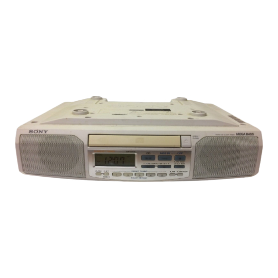
Fm/am cd kitchen clock radio
Hide thumbs
Also See for ICF-CD513:
- Operating instructions (2 pages) ,
- Brochure (2 pages) ,
- Operating instructions (2 pages)
Table of Contents
Advertisement
SERVICE MANUAL
Ver 1.1 2003. 08
CD player section
System: Compact disc digital audio system
Laser diode properties: Material: GaAlAs
Wavelength: 780 nm
Emission duration: Continuous
Laser output: Less than 44.6 µW
(This output is the value measured at a
distance of about 200 mm from the objective
lens surface on the optical pick-up block with
7 mm aperture.)
Frequency response: 20-20 000 Hz
Wow and flutter: Below measurable limit
Radio section
Frequency range:
US, Canadian models
Band
Frequency range
FM
87.5-108 MHz
AM
530-1 710 kHz
AEP model
Band
Frequency range
FM
87.5-108 MHz
AM
531-1 602 kHz
FM
87.5-108 MHz
AM
530-1 610 kHz
Sony Corporation
9-927-968-12
2003H05-1
Personal Audio Company
C 2003.08
Published by Sony Engineering Corporation
Model Name Using Similar Mechanism
CD Mechanism Type
Optical Pick-up Block Name
Optical Pick-UP Name
SPECIFICATIONS
+1
dB
–1.5
Channel step
0.1 MHz
10 kHz
Channel step
0.05 MHz
9 kHz
0.1 MHz
10 kHz
FM/AM CD KITCHEN CLOCK RADIO
ICF-CD513
General
Time display:
US, Canadian models: 12-hour system
AEP model: 24-hour system
Speaker:
5
66 mm (2
⁄
inches) dia., 4 Ω
8
Power outputs:
1.2 W + 1.2 W
(at 10% harmonic distortion)
Power requirements:
US, Canadian models: 120 V AC, 60 Hz
AEP model: 220-230 V AC, 50 Hz
Dimensions:
Approx. 365 × 106 × 281 mm (w/h/d)
3
1
1
(Approx. 14
⁄
× 4
⁄
× 11
⁄
inches) incl.
8
4
8
projecting parts and controls
Mass:
Approx. 2.9 kg (6 lb. 6 oz.)
Supplied accessories:
Mounting screws (4), Template (1),
Spacers (4), Cord clamp (1)
Design and specifications are subject to change
without notice.
US Model
Canadian Model
AEP Model
ICF-CD533
KSL-213BGN (FORMER)
FLM-CD513-149 (NEW)
KSM-213BGN (FORMER)
KSM-213RCP (NEW)
KSS-213B (FORMER)
KSS-213R (NEW)
Advertisement
Table of Contents

Related Manuals for Sony ICF-CD513


Summary of Contents for Sony ICF-CD513
- Page 1 Design and specifications are subject to change 87.5-108 MHz 0.05 MHz without notice. 531-1 602 kHz 9 kHz 87.5-108 MHz 0.1 MHz 530-1 610 kHz 10 kHz FM/AM CD KITCHEN CLOCK RADIO Sony Corporation 9-927-968-12 2003H05-1 Personal Audio Company C 2003.08 Published by Sony Engineering Corporation...
-
Page 2: Table Of Contents
SUR LES DIAGRAMMES SCHÉMATIQUES ET LA LISTE DES PIÈCES SONT CRITIQUES POUR LA SÉCURITÉ DE FONCTIONNEMENT. NE REMPLACER CES COM- POSANTS QUE PAR DES PIÈCES SONY DONT LES NUMÉROS SONT DONNÉS DANS CE MANUEL OU DANS LES SUPPLÉMENTS PUBLIÉS PAR SONY. -
Page 3: Servicing Notes
10.64 MHz white 10.76 MHz MODEL IDENTIFICATION – Top View – MODEL NO. ICF-CD513 US, Canadian models: AC: 120 V 60 Hz 15 W AEP model: AC: 220 – 230 V 50 Hz 15 W – 3 –... -
Page 4: General
SECTION 2 This section is extracted from instruction manual. GENERAL Press CLOCK once. Features AC power cord Cord clamp The minute will flash. Cordon d’alimentation secteur Attache de cordon • Built-in CD player with Shuffle/Repeat function. • PLL (Phase Locked Loop) Synthesized Tuner with 15 memory presets for easy one button tuning. -
Page 5: Operating The Radio
Tuning in to a preset station Adjust volume using VOLUME . Operating the Radio Press RADIO ON•BAND to turn on the Press radio. Manual Tuning Pause CD u Press RADIO ON•BAND to select the Resume play after CD u again Press RADIO ON•BAND to turn on the band. -
Page 6: Disassembly
SECTION 3 DISASSEMBLY • This set can be disassembled in the order shown below. CD MECHANISM DECK CABINET (UPPER) CABINET FRONT ASSY MAIN BOARD (KSL-213BGN) MOTOR BOARD, OPTICAL LOADING MOTOR BOARD PICK-UP SECTION Note: Follow the disassembly procedure in the numerical order given. CABINET (UPPER) 5 eight screws (BTP3 ×... - Page 7 CD MECHANISM DECK (KSL-213BGN) 7 CD mechanism deck (KSL-213BGN) boss 3 connector (CN701) 6 chassis NOTE: On installation of CD mechanism deck, cut the boss. 5 four screws (BTP3 × 10) 4 wire (flat type) (16core) 1 connector (CN503) MAIN BOARD 1 connector 1 connector (CN301) (KH901)
- Page 8 MOTOR BOARD, LOADING MOTOR BOARD 1 Remove two solders. 3 MOTOR board 2 LOADING MOTOR board 1 Remove two solders. 1 Remove two solders. OPTICAL PICK-UP SECTION 1 two screws (BVTT3 × 6) 7 four screws (2.6 × 16) 3 holder (MG) assy 2 two claws 6 disc table 8 optical pick-up section...
-
Page 9: Test Mode
SECTION 4 TEST MODE 4-1. LCD TEST MODE 4-2. CD TEST-1 (AUTO) MODE [Setting the Test Mode] [Setting the Test Mode] [ALARM • Turn the power on while pressing + > • Short the solder bridge of BP404 on the MAIN board (connect ON/OFF] buttons simultaneously. - Page 10 4-3. CD TEST-2 (MANUAL) MODE [Setting the Test Mode] • Short the solder bridge of BP403 on the MAIN board (connect IC401 tk pin and ground) and turn the power on. [Operation of Test Mode] 1. Insert the CD test disc YEDS-18. (Parts No. 3-702-101-01) 2.
-
Page 11: Electrical Adjustments
SECTION 5 ELECTRICAL ADJUSTMENTS no mark : US, Canadian models TUNER SECTION 0 dB=1 µV < > : AEP model [AM] AM IF ADJUSTMENT Setting: Adjust for a maximum reading on level meter Function : RADIO 450 kHz Band switch : AM Put the lead-wire AM FREQUENCY COVERAGE ADJUSTMENT AM RF signal... -
Page 12: Cd Section
CD SECTION CD section adjustments are done automatically in this set. In case of operation check, confirm that focus bias. Focus Bias Check Connection: oscilloscope (AC range) MAIN board TP513 (RF) – TP568 (GND) Procedure: 1. Connect the oscilloscope to TP513 (RF) and TP568 (GND) on the MAIN board. - Page 13 Adjustment Location and Connecting Points FM Tracking Adjustment – MAIN BOARD (Component Side) – L4 AM Frequency Coverage Adjustment AM Tracking Adjustment RV1 FM VCO Adjustment L2 FM Frequency T1 AM IF Adjustment Coverage Adjustment – MAIN BOARD (Conductor Side) – IC551 IC501 TP513...
-
Page 14: Diagrams
ICF-CD513 SECTION 6 DIAGRAMS 6-1. BLOCK DIAGRAM – CD Section – MAIN BOARD (1/3) FILTER DIGITAL SIGNAL PROCESSOR, CLV SERVO, D/A CONVERTER IC551 ERROR CN501 CORRECTOR PD1 I-V AMP PCMD PCMDI DETECTOR BCKI OVER ASYMMETRY SERIAL SUMMING DIGITAL PLL SAMPLING... -
Page 15: Block Diagram - Tuner Section
6-2. BLOCK DIAGRAM – TUNER Section – MAIN BOARD (2/3) 10.7MHz FM/AM FRONT-END, FM/AM DET, MPX FM RF FM/AM L-CH OUT TUNER L-CH 10.7MHz FE OUT B.P.F. IF IN FM IF AMP/ DECODER R-CH OUT TUNER R-CH BPF1 FRONT-END DISCRI TO MAIN FROM MAIN SECTION... -
Page 16: Block Diagram - Main Section
ICF-CD513 6-3. BLOCK DIAGRAM – MAIN Section – MAIN BOARD (3/3) VOLUME BOARD POWER AMP IC351 CN303 W301 W301 CN303 CN301 (2/2) (1/2) (2/2) (2/2) LINE FROM CD LINE AMP MEGA BASS FILTER L-CH/R-CH L-CH SP101 SECTION (FOR CD) Q105... - Page 17 ICF-CD513 6-4. PRINTED WIRING BOARDS • Circuit Boards Location MAIN BOARD POWER BOARD KEY BOARD S415 POWER board S413 D. S. T. S406 LOADING board S409 CN401 S404 S412 S408 S403 L901 ALARM SUMMER T. CLOCK CN901 L902 KH901 LED board...
-
Page 18: Schematic Diagram - Main (1/4)/Key/Led Boards
ICF-CD513 6-5. SCHEMATIC DIAGRAM – MAIN (1/4)/KEY/LED Boards – • See page 35 for Waveforms. (Page 29) (Page 33) (Page 31) Note on Schematic Diagram: • All capacitors are in µF unless otherwise noted. pF: µµF • Voltages are taken with a VOM (Input impedance 10 MΩ). -
Page 19: Schematic Diagram - Main Board (2/4)
ICF-CD513 6-6. SCHEMATIC DIAGRAM – MAIN Board (2/4) – • • See page 35 for Waveform. See page 36 for IC Block Diagrams. (Page 28) (Page 33) Note on Schematic Diagram: • All capacitors are in µF unless otherwise noted. pF: µµF •... -
Page 20: Schematic Diagram - Main (3/4)/Loading/Motor Boards
ICF-CD513 6-7. SCHEMATIC DIAGRAM – MAIN (3/4)/LOADING/MOTOR Boards – • • See page 35 for Waveforms. See page 37 for IC Block Diagrams. (Page 28) (Page 33) Note on Schematic Diagram: • A : B+ Line. • All capacitors are in µF unless otherwise noted. pF: µµF •... -
Page 21: Schematic Diagram - Main (4/4)/Volume/Power Boards
ICF-CD513 6-8. SCHEMATIC DIAGRAM – MAIN (4/4)/VOLUME/POWER Boards – (Page 30) (Page 28) (Page 32) Note on Schematic Diagram: • All capacitors are in µF unless otherwise noted. pF: µµF 50 WV or less are not indicated except for electrolytics and tantalums. - Page 22 • Waveforms – MAIN board – 5 IC501 w; (CLK), IC551 qf (CLKO) 9 IC551 el (LRCK) (CD PLAY mode) 1 IC401 yk (X2) (CD PLAY mode) (CD PLAY mode) 2 V/DIV, 5 µs/DIV 1 V/DIV, 100 ns/DIV 2 V/DIV, 2 µs/DIV 5.1 Vp-p 3.9 Vp-p 5.6 Vp-p...
- Page 23 • IC Block Diagrams – MAIN Board – IC1 CXA1238M-T6 FM FRONT-END AM FRONT-END REGULATOR FM IF/ DISCRI REGULATOR AM IF/ COUNTER COUNTER AUTO TUNING BLEND INDICATOR MONO/STEREO MUTING SELECT BAND-PASS MUTE RIPPLE DECORD FILTER 11 12 13 14 15 IC51 BU2614FS MAIN CONTROL PHASE...
- Page 24 IC501 CXA1992BR 33 32 31 30 PD 2 PD 1 I-V AMP I-V AMP RF SUMMING FOCUS OK COMPARATOR LASER POWER CONTROL IFB1 – IFB6 PEAK/BOTTOM MIRR HOLD COMPARATOR ↓ DEFECT PEAK/BOTTOM BIAS HOLD FOCUS BIAS FOCUS ERROR WINDOW COMPARATOR F I-V SENS2 ↓...
- Page 25 IC551 CXD2589Q 59 58 57 54 53 52 51 SYSM SERIAL-IN INTERFACE LRCKI LRCK AVSS OVER SAMPLING ASYO DIGITAL FILTER ASYI ASYMMETRY DEMODULATOR CORRECTOR BIAS AVDD 3rd-ORDER AVDD NOISE SHAPER AOUT1 AIN1 CLTV LOUT1 AVSS ERROR XVDD CORRECTOR AVSS XTAI SUB CODE PROCESSOR DIGITAL...
- Page 26 IC591 BA6898FP LEVEL SHIFT LEVEL SHIFT – – – REGULATOR DRIVER BIAS, T. S. D MUTE MONITOR LEVEL SHIFT LEVEL SHIFT 3 4 5 6 9 10 12 13 IC701 BA6208 MOTOR SWITCH DRIVE MOTOR SWITCH DRIVE – 39 –...
-
Page 27: Ic Pin Function Description
6-9. IC PIN FUCTION DESCRIPTION • MAIN BOARD IC401 µPD789406AGC-017-8BT (SYSTEM CONTROLLER) Pin No. Pin Name Description VDD1 — Power supply terminal (+5V) BIAS Bias output for the liquid crystal display drive 3 to 5 VLC0 to VLC2 — Terminal for doubler circuit capacitor connection to develop liquid crystal display drive voltage VSS1 —... - Page 28 Pin No. Pin Name Description VSS0 — Ground terminal VDD0 — Power supply terminal (+5V) Sub system clock output terminal (32.768 kHz) Sub system clock input terminal (32.768 kHz) — Internal connection terminal (connected to ground) TRAY OPEN Motor drive signal output to the loading motor drive (IC701) “H” active *1 TRAY CLOSE Motor drive signal output to the loading motor drive (IC701) “H”...
-
Page 29: Exploded Views
SECTION 7 EXPLODED VIEWS NOTE: • -XX and -X mean standardized parts, so they • Items marked “*” are not stocked since they The components identified by mark 0 or dotted line with mark are seldom required for routine service. Some may have some difference from the original 0 are critical for safety. - Page 30 (2) CABINET (LOWER) not supplied not supplied SP202 main board LCD401 SP201 SP102 not supplied not supplied T901 SP101 supplied US, Canadian The components identified by Les composants identifiés par une mark 0 or dotted line with marque 0 sont critiques pour la mark 0 are critical for safety.
- Page 31 (3) CD BLOCK SECTION (KSL-213BGN) not supplied KSM-213BGN M480 Ref. No. Part No. Description Remark Ref. No. Part No. Description Remark * 201 X-2625-879-1 HOLDER (BU) ASSY 2-627-163-01 GEAR (P) * 202 1-656-254-11 LOADING BOARD 4-927-649-01 BELT 3-931-379-01 RUBBER, VIBRATION PROOF 2-627-172-01 PULLEY (S) 3-916-006-01 SCREW (2.6X16) 2-627-162-01 GEAR (C)
- Page 32 (4) OPTICAL PICK-UP SECTION (KSM-213BGN) not supplied not supplied M592 The components identified by Les composants identifiés par une mark 0 or dotted line with marque 0 sont critiques pour la mark 0 are critical for safety. sécurité. Replace only with part num- Ne les remplacer que par une pièce ber specified.
-
Page 33: Electrical Parts List
SECTION 8 LOADING MAIN ELECTRICAL PARTS LIST NOTE: • Due to standardization, replacements in the • Items marked “*” are not stocked since they The components identified by mark 0 or dotted line with mark are seldom required for routine service. parts list may be different from the parts speci- 0 are critical for safety. - Page 34 MAIN Ref. No. Part No. Description Remark Ref. No. Part No. Description Remark 1-162-927-11 CERAMIC CHIP 100PF C351 1-162-970-11 CERAMIC CHIP 0.01uF 1-162-927-11 CERAMIC CHIP 100PF 1-164-315-11 CERAMIC CHIP 470PF C352 1-164-227-11 CERAMIC CHIP 0.022uF 1-162-964-11 CERAMIC CHIP 0.001uF C353 1-126-963-11 ELECT 4.7uF C356...
- Page 35 MAIN Ref. No. Part No. Description Remark Ref. No. Part No. Description Remark C508 1-164-677-11 CERAMIC CHIP 0.033uF C580 1-104-665-11 ELECT 100uF C509 1-104-509-11 CERAMIC CHIP 0.018uF C510 1-162-915-11 CERAMIC CHIP 10PF 0.5PF C581 1-162-970-11 CERAMIC CHIP 0.01uF C511 1-126-962-11 ELECT 3.3uF C582 1-107-826-11 CERAMIC CHIP...
- Page 36 MAIN Ref. No. Part No. Description Remark Ref. No. Part No. Description Remark < DIODE > < COIL > 8-713-100-11 DIODE 1T362 1-406-545-11 COIL, AIR-CORE 8-713-100-11 DIODE 1T362 1-416-459-11 COIL, AIR-CORE 8-719-072-59 DIODE SVC347S-TL 1-402-616-11 ANTENNA, FERRITE-ROD (AM) D301 8-719-074-44 DIODE 1SS120RX 1-406-485-11 COIL (OSC) D302 8-719-074-44 DIODE 1SS120RX...
- Page 37 MAIN Ref. No. Part No. Description Remark Ref. No. Part No. Description Remark 1-216-821-11 METAL CHIP 1/16W R256 1-216-839-11 METAL CHIP 1/16W 1-216-833-11 RES, CHIP 1/16W R301 1-216-841-11 METAL CHIP 1/16W R302 1-216-817-11 METAL CHIP 1/16W 1-216-833-11 RES, CHIP 1/16W R303 1-216-834-11 METAL CHIP 1/16W...
- Page 38 MAIN Ref. No. Part No. Description Remark Ref. No. Part No. Description Remark R444 1-216-821-11 METAL CHIP 1/16W R525 1-216-845-11 METAL CHIP 100K 1/16W R445 1-216-845-11 METAL CHIP 100K 1/16W R446 1-216-821-11 METAL CHIP 1/16W R526 1-216-845-11 METAL CHIP 100K 1/16W R447 1-216-821-11 METAL CHIP...
- Page 39 ICF-CD513 MAIN MOTOR POWER VOLUME Ref. No. Part No. Description Remark Ref. No. Part No. Description Remark < VARIABLE RESISTOR > R217 1-216-853-11 METAL CHIP 470K 1/16W R228 1-216-809-11 METAL CHIP 1/16W 1-241-765-11 RES, ADJ, CARBON 22K R229 1-216-829-11 METAL CHIP 4.7K...
- Page 40 ICF-CD513 US Model Canadian Model SERVICE MANUAL AEP Model Ver 1.1 2003.08 SUPPLEMENT-1 File this supplement with the service manual. Subject: Change of CD MECHANISM BLOCK KSL-213BGN → FLM-CD513-149 (ENG-03044) In this set, from the production middle CD mechanism deck section from KSL-213BGN it is changed into FLM-CD513-149.
- Page 41 ICF-CD513 NEW/FORMER TYPE DISCRIMINATION FORMER TYPE NEW TYPE Serial No. 0105500 before (US) Serial No. 0105501 after (US) Serial No. 0107100 before (Canadian) Serial No. 0107101 after (Canadian) Serial No. 0110385 before (AEP) Serial No. 0110386 after (AEP) FRONT SIDE...
- Page 42 ICF-CD513 DISASSEMBLY • This set can be disassembled in the order shown below. 2-1. DISASSEMBLY FLOW Note 1: The process described in can be performed in any order. Note 2: Without completing the process described in , the next process can not be performed.
- Page 43 ICF-CD513 2-3. TRAY 2 claw 1 Turn the drive gear in the direction of the arrow A . 2 claw 4 tray 2-4. BELT, LOADING BOARD 1 belt 2 two screws (M2 × 3) 3 claw 3 claw 4 loading board...
- Page 44 ICF-CD513 2-5. BASE UNIT 1 two screws (PWH2.6 × 10) 2 boss 4 base unit 3 boss 2 boss 2-6. ARM, OPTICAL PICK-UP SECTION (KSM-213RCP) 2 arm 4 vibration proof rubber (red) 4 vibration proof rubber 3 vibration proof rubber...
- Page 45 ICF-CD513 2-7. OPTICAL PICK-UP (KSS-213R) 1 gear (B) 5 optical pick-up (KSS-213R) 4 sled shaft 2 two screws (M2)
- Page 46 ICF-CD513 PRINTED WIRING BOARD – LOADING Board – M480 (LOADING) LOADING BOARD C708 L703 L702 S701 TRAY CN701 OPEN/CLOSE DETECT MAIN BOARD W701 (11) 1-689-833- SCHEMATIC DIAGRAM – LOADING Board – C708 L703 47µH M480 (LOADING) CN701 L702 47µH OP-HO...
- Page 47 ICF-CD513 5. EXPLODED VIEWS NOTE: • Items marked “*” are not stocked since they • -XX and -X mean standardized parts, so they The components identified by mark 0 or dotted line with mark may have some difference from the original are seldom required for routine service.
- Page 48 ICF-CD513 5-2. CD MECHANISM DECK SECTION (FLM-CD513-149) not supplied not supplied base unit section not supplied M480 Ref. No. Part No. Description Remark Ref. No. Part No. Description Remark 3-028-010-02 TRAY 3-921-725-11 SCREW (2.6X10), +PWH 3-028-019-02 PLATE, CHUCK * 509...
- Page 49 ICF-CD513 5-3. BASE UNIT SECTION (FLM-CD513-149) optical section (KSM-213RCP) Ref. No. Part No. Description Remark Ref. No. Part No. Description Remark 3-028-011-01 ARM 3-921-725-01 SCREW (2.6X10), +PWH 3-910-095-31 RUBBER, VIBRATION PROOF (GREEN) 3-910-095-21 RUBBER, VIBRATION PROOF (RED)
- Page 50 ICF-CD513 5-4. OPTICAL BLOCK (KSM-213RCP) M592 The components identified by Les composants identifiés par une mark 0 or dotted line with marque 0 sont critiques pour la mark 0 are critical for safety. sécurité. Replace only with part num- Ne les remplacer que par une pièce ber specified.
- Page 51 ICF-CD513 LOADING 6. ELECTRICAL PARTS LIST NOTE: • Items marked “*” are not stocked since they • Due to standardization, replacements in the The components identified by 0 or dotted line with mark mark are seldom required for routine service.
- Page 52 ICF-CD513 Printing Method for Large Sized Documents Such As Circuit Diagrams Printing the page that exceeds A4-size two pages (or letter size) is possible by specifying the print range. (Acrobat Reader Version 4.0 or later) 1. The enlarged print is made, if a smaller range than A4 size is specified and the A4 size is selected as a print paper.
- Page 53 ICF-CD513 REVISION HISTORY Clicking the version allows you to jump to the revised page. Also, clicking the version at the upper right on the revised page allows you to jump to the next revised page. Ver. Date Description of Revision 2000.07...
Need help?
Do you have a question about the ICF-CD513 and is the answer not in the manual?
Questions and answers