Casio CE-300 (EX-247) Service Manual
Electronic cash register
Hide thumbs
Also See for CE-300 (EX-247):
- Service manual (53 pages) ,
- Most important functions (5 pages)

Related Manuals for Casio CE-300 (EX-247)


Summary of Contents for Casio CE-300 (EX-247)
- Page 1 SERVICE MANUAL (without price) ELECTRONIC CASH REGISTER CE-300 (EX-247) JANUARY 1997 Printer Model : MD-910...
-
Page 2: Table Of Contents
CONTENTS Page 1. SPECIFICATIONS ....................1 2. INITIALIZE (MAC) OPERATION ................1 3. BLOCK DIAGRAM 3-1. PCB connection ..................2 3-2. Block diagram (circuit) ................3 4. CIRCUIT EXPLANATION 4-1. Power supply circuit .................. 4 4-2. CPU (uPD78052GC-093-3B9) ..............5 4-3. -
Page 3: Specifications
1. SPECIFICATIONS Power consumption 120 V 220 V 230 V 240 V In operation Max. 0.28 A 0.17 A 0.16 A 0.15 A Stand by 0.14 A 0.09 A 0.08 A 0.07 A Mode SW OFF Max. 0.12 A 0.08 A 0.07 A 0.06 A Memory protection... -
Page 4: Block Diagram
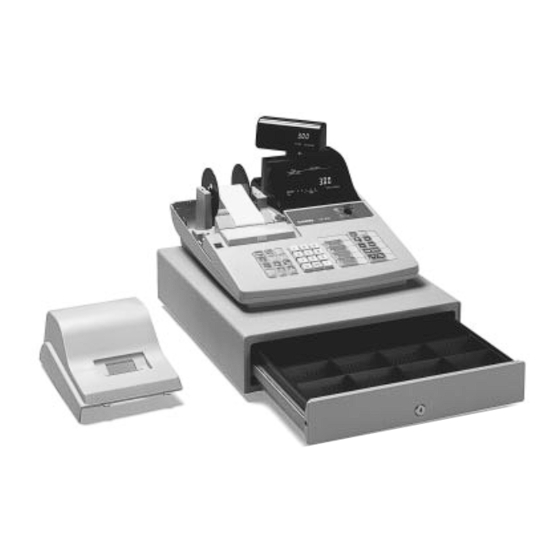
3. BLOCK DIAGRAM 3-1. PCB connection Transformer Rear Display (SH1019A) E278-E2-2 Fuse Main Display Mangan Battery (SH101MA) (UM-3 × 3) E278-E2-1 Winder Motor E247-CNB Printer (MD910SSC) CN13 E247-1 CN14 CORE 2 turn Drawer (RS232C) CN16 CN17 Mode SW E266-E3-1 — 2 —... -
Page 5: Block Diagram (Circuit)
3-2. Block diagram (circuit) Reset circuit MAIN DISPLAY CUSTOMER DISPLAY SH101MA Printer SH1019A S80719AN MD-910 Segment & Digit data Head drive cuicuit HD.A~HD.H uPD16312GB- DRWS uPD78052GC-093-3B9 DI,DO,CLK,STB KC0~KC4 Select addess Keyboard AD0~AD5 Mode A8~A15 AD0~AD7 PWD detection A0~A7 RS232C circuit —... -
Page 6: Circuit Explanation
4. CIRCUIT EXPLANATION 4-1. Power supply circuit Q1: Power transistor Q2: Voltage detection transistor Voltage level at above check point (unit: V ) Measurement position Voltage (V) 12.5V 5.3V 6.2V 2.47V — 4 —... -
Page 7: Cpu (Upd78052Gc-093-3B9)
4-2. CPU (uPD78052GC-093-3B9) Status of Status of Pin No. Signal Description I n / O u t Power On Power OFF 1 FB3 Not used — — — 2 FB4 RAM bank 3 High High 3 FB5 RAM bank 4 High High 4 AVSS... - Page 8 Status of Status of Pin No. Signal Description I n / O u t Power On Power OFF 56 HD.E Head drive signal of printer (HD.E) 57 HD.F Head drive signal of printer (HD.F) 58 HD.G Head drive signal of printer (HD.G) 59 HD.H Head drive signal of printer (HD.H) 60 RESET...
-
Page 9: Display Controller (Upd16312Gb-3B4)
4-3. Display controller (uPD16312GB-3B4) Status of Status of Pin No. Signal Description I n / O u t Power On Power OFF 1 SW1 Not used (GND) — 2 SW2 Not used (GND) — 3 SW3 Not used (GND) — 4 SW4 Not used (GND) —... -
Page 10: Initialize Ic (Reset Circuit)
4-4. Initilize IC (Reset circuit) VDD: Voltage of memory protection battery To Pin No.60 of CPU When the voltage level at Pin No.60 of CPU is not stabilized, CPU does not work properly in rare case. Therefore, this machine uses the initialize IC for stabilizing the voltage. Even the voltage level of VDD (Pin No.2) is changed, Pin No.1 of initilize IC outputs stabilized 5 volts. -
Page 11: Ram / Rom Bank Selection Circuit
4-7. RAM / ROM bank selection circuit This circuit is used for address decoder for memory. RAM 1 M RAM 256 K Memory Map 00001 00011 00101 000000 00100 11101 00010 00110 0000 Mask ROM Bank Bank Bank Bank Bank Bank Bank (16 K) -
Page 12: Head Drive Circuit For Printer
4-8. Head drive circuit for printer TR4 TR3 Motor drive circuit Normally, the transistor of motor drive circuit is followng condition. TR1, TR2, TR5 : TR3, TR4 : MD (-) signal : VP level When the CPU want to rotate the motor, CPU change the MD signal to “High” from “Low”. Then, TR1, TR2 and TR5 are become ON and MD (-) signal is become GND level, and then motor is rotated. -
Page 13: Vpp Sensor Circuit
4-9. VPP sensor circuit Protection circuit To prevent the circuit breakage, the protection circuit watches the voltage level of VCC, VDD and VPP. When the each voltage level is more than following condition, this circuit cuts the voltage. VCC,VDD: In case these voltages are become over voltage, this circuit outputs “SCR” signal(High signal) and burn out the fuse. -
Page 14: Diagnostic
5. DIAGNOSTIC 5-1. To start the diagnostic program 1. Set the mode switch to “OFF” position. 2. Pressing the “FEED” button and turn the mode switch to “PRG” position. 3. Release the “FEED” button. 4. Input “9999900000” and press “ST” (“#2” key). 5. - Page 15 2. Switch status test Press “C” button, the switch status is appeared on the display. [DISPLAY] No display No display No display No display Low battery L: Low battery Nil: Battery OK PAD2 status 1: Short 0: Open PAD1 status 1: Short 0: Open Always: 1...
- Page 16 3. Individual function test 3-1. Series test “Y” “X” “1” + “#2” key 0: Normal test 1: Execute next test even if an error happend at ROM check sum 0: Autockecking of RAM capacity 1: 256 Kbit RAM test 2: 1 Mbit RAM test Execute the following test in order.
- Page 17 3-2. Print test Input “Y” “X” “2” + “#2” key. 0: Print the following character continuously. Printing speed : 45 times / Min. 1: Print the following character, open the drawer and issue a receipt Printing speed : 25 times / Min. Drawer open : 5 times / Min.
- Page 18 3-6. All character print test Input “8” + “#2” key. “8” + “#2”: Pirnts all character on receipt once. “1” “8” + “#2”: Prints all character on receipt continuously. To stop this test, press any key or turn the mode switch to “OFF” position. 3-7.
-
Page 19: To Exit The Diagnostic Test
3-8. RS232C port test Input “2” “0” “7” + “#2” key. Execute the RS232C loop back test continuously using loop back connector. In case an error happens, the machine issues an error receipt then stop this test. Test description: 1: Level check at DSR signal ( Low/High) 2: Send the data (05Ah) from TxD and receive it at RxD terminal. -
Page 20: Error Code
6. ERROR CODE 6-1. Operation error code Error codes appear on display whenever you make a mistake during operation. Error Code Meaning Action Mode switch position changed before finalization. Return the mode switch to its original setting and finalize the operation. Registration without entering a clerk number. -
Page 21: System Lock Code
6-2. System lock code The following error code appears on display and receipt when the machine is lock up. Execute the Flag MAC or MAC operation to clear these errors. Error code: Display: X - - - - - - - - - Receipt: X ! ! ! ! ! ! ! ! ! ! ! ! ! ! ! ! ! ! X: Lock code... -
Page 22: Ic Data
7. IC DATA 1. TC74HC00AP 2. TC74HC08AP 3. TC74HC138 — 20 —... -
Page 23: Tc74Hc367Ap
4. TC74HC367AP 5. TL431CLPB 6. TC74HC373AP — 21 —... -
Page 24: Max232
7. S-80745 / S-80719 8. M5237L tion protec Heat OP AMP protection Voltage adjust Start up STD. Voltage Current protection Terminal Voltage adjust 9. MAX232 — 22 —... -
Page 25: Pcb Layout
8. PCB LAYOUT MAIN PCB (E247-1) and Connector PCB (E247-CNB) — 23 —... -
Page 26: Circuit Diagrams
9. CIRCUIT DIAGRAMS Description: Board No. Drawing No. LOCATION OF PRINTED E240450 CIRCUIT BOARDS — 25 —... - Page 27 PAD condition B.D.Bu PAD1 Open Short Description: Board No. Drawing No. PAD2 MAIN PCB E247-1 (1/8) E240451 Short Short — 26 —...
- Page 28 Description: Board No. Drawing No. MAIN PCB E247-1 (2/8) E240452 — 27 —...
- Page 29 Description: Board No. Drawing No. MAIN PCB E247-1 (3/8) E240453 — 28 —...
- Page 30 Description: Board No. Drawing No. MAIN PCB E247-1 (4/8) E240454 — 29 —...
- Page 31 Description: Board No. Drawing No. MAIN PCB E247-1 (5/8) E240455 — 30 —...
- Page 32 Description: Board No. Drawing No. MAIN PCB E247-1 (6/8) E240456 — 31 —...
- Page 33 Description: Board No. Drawing No. MAIN PCB E247-1 (7/8) E240457 — 32 —...
- Page 34 Description: Board No. Drawing No. MAIN PCB E247-1 (8/8) E240458 — 33 —...
- Page 35 Description: Board No. Drawing No. E247-CNB E247-CNB E440522 — 34 —...
- Page 36 Description: Board No. Drawing No. KEYBOARD E240465 — 35 —...
- Page 37 Description: Board No. Drawing No. MAIN DISPLAY E278-E2-1 E440523 — 36 —...
- Page 38 Description: Board No. Drawing No. CUSTOMER DISPLAY E278-E2-2 E440524 — 37 —...
- Page 39 Description: Board No. Drawing No. POWER SUPPLY CIRCUIT E340638 — 38 —...
- Page 40 Description: Board No. Drawing No. BATTERY E440525 — 39 —...
-
Page 41: Parts List
10. PARTS LIST 1. Main PCB block E247-1 ass’y ..............43 2. Main display block E247-E2-1 ..............47 3. Customer display block E247-E2-2 ............47 4. Button ass’y....................48 5. Upper case ass’y ..................48 6. Lower case ass’y ..................48 7. - Page 42 — 43 —...
- Page 43 — 44 —...
-
Page 44: Main Pcb Block E247-1 Ass'y
CE-300 Item Code No. Parts Name Specification Version 1. Main PCB block E247-1 ass’y 6193 4726 Main PCB ass'y E247-1 E240425*2 All countries 2006 1207 LSI UPC16312GB-3B4 IC11 2006 1655 LSI UPD78052GC-093-3B9 IC14 2006 1354 LSI TMS27C512-12/15JL IC15 2006 1319 RAM CXK58275AP-70/10L IC26 2101 0189 MOS IC... - Page 45 Item Code No. Parts Name Specification Version R10,19,43 Carbon film resistor CR-25-100OHMJ-T 20 X R52-54, R84,85,94, R99,100, R103-105, R108,109, R128-131 R86,111, Carbon film resistor CR-25-1KOHMJ-T R112,116, R118 R33,47,87 Carbon film resistor CR-25-4.7KOHMJ-T R6,9,11, Carbon film resistor CR-25-10KOHMJ-T 18 X R20,23,46 R88,89,93, R95,96,98, R106,107,...
-
Page 46: Main Display Block E247-E2-1
Item Code No. Parts Name Specification Version C17-18, Ceramic capacitor RT-HE40TKYB101K 18 X C26,29, C31-32, C48-51, C53-54, C56-60,64 Ceramic capacitor RT-HE40TKYB471K C24,35, Ceramic capacitor RT-DSTB90TKYR104K 11 X C41-42,46, C61-63, C65-67 Ceramic capacitor RT-HE40TKCH120J Ceramic capacitor RT-HE40TKCH150J C5,12,13, Film capacitor AMZV0050K1040200 C25,47 C8,37 CERAMIC DISC CAP... -
Page 47: Button Ass'y
Item Code No. Parts Name Specification Version 3540 4913 PCB connector 52045-1245 6246 4270 Display spacer E412178-1 6246 4310 Display cushion B E412177-2 6247 6469 Customer display case E240325-1 6248 0515 Rear display panel E240326-4 4. Button ass’y 6192 4970 Mode key switch ass'y E311944*1 6284 0844 Mode key plate E440460-1... -
Page 48: Total Component
Item Code No. Parts Name Specification Version 3700 4281 Power cord PS204 Other countries 6221 4802 Power cord M2511 Germany, Europe 6248 0396 Lower case E247 E140118-4 6248 0779 FG plate E340646-1 6248 0873 Connector fixing plate E247 E340524-1 Screw with washer 3X8 ZMC-3 Tapping screw with washer 4X8 ZMC-3... -
Page 49: Cash Drawer (Dl-2763)
8. Cash drawer (DL-2763) — 50 —... - Page 50 Item Code No. Parts Name Specification Version 8. Cash drawer (DL-2763) 6247 9752 Cash drawer (DL-2763) E440128A*14 6192 7953 Bill/Coin case ass'y E140034*3 6247 3935 Coin case E140058-1 6246 5230 Bill holder fixing plate E211620-1 6247 3949 Coin separeter E340173-1 6246 5220 Bill holder spring E412160-1 6221 4902 Bill holder...
-
Page 51: Printer
9. Printer (MD-910) — 52 —... - Page 52 MD-910 Item Code No. Parts Name Specification 1904 7581 Frame NC44701-07 1904 7582 Gear box sub ass'y NC10701-00 2-10,5-6 1906 2087 E-Ring,2 E60320-00 1904 7583 Cylinder cam NC19701-00 1904 7584 Bushing for cam shaft NC21201-01 1904 7585 Paper feeding gear NC20201-02 1904 7586 Gear for paper feed cam NC20202-03...
- Page 53 Item Code No. Parts Name Specification 11-3 1904 7635 Knob NC20208-01 11-4 1904 7636 Gear for PF drive NC20209-01 11-5 1904 7637 Gear for idler NC20210-00 11-6 1906 2087 E-Ring, 2 E60320-00 12-1 1904 7638 Gear A for knob NC20205-01 12-2 1904 7639 Gear B for knob NC20206-03...
- Page 54 MA0301571A...
Need help?
Do you have a question about the CE-300 (EX-247) and is the answer not in the manual?
Questions and answers