
Related Manuals for Hisense 40LE45S


Summary of Contents for Hisense 40LE45S
- Page 1 LCD Television Service Manual Chassis: MT5380 Product Type: 40LE45S、40LC45S Ver 1.0 Hisense Electric Co.,Ltd. March,2009...
-
Page 2: Table Of Contents
7.5 Troubleshooting for TV/VGA/HDMI input..................- 30 - 7.6 Troubleshooting for YPbPr input......................- 31 - 7.7 Troubleshooting for Video/S-Video input.....................- 32 - 8. Explode View and Explode Bom List......................- 33 - 9. Schematic circuit diagram ..........................- 33 - Hisense Confidential - 2 -... -
Page 3: Service Manual
WHEN REPLACEMENT PARTS ARE REQUIRED, BE SURE TO USE REPLACEMENT PARTS SPECIFIED BY THE MANUFACTURER. Proper service and repair is important to the safe, reliable operation of all Hisense Electric Co., Ltd Equipment. The service procedures recommended by Hisense and described in this Service Guide are effective methods of performing service operations. -
Page 4: Warning
Hisense, must first satisfy himself thoroughly that neither his safety nor the safe of the equipment will be jeopardized by the service method selected. Hereafter throughout this manual, Hisense Electric Co., Ltd will be referred to as Hisense. 1.1 Warning 1.1.1... - Page 5 In particular attention should be paid to the following points. -Note: The wire trees should be routed correctly and fixed with the mounted cable clamps. -The insulation of the mains lead should be checked for external damage. 1.1.6 Hisense Confidential - 5 -...
- Page 6 (7) Do not pull out or insert the power cable from/to an outlet with wet hands. It may cause electric shock. (8) Do not damage or modify the power cable. It may cause fire or electric shock. Hisense Confidential - 6 -...
-
Page 7: Notes
2 minutes after the main power has been turned off. • While the main power is on, do not touch any parts or circuits other than the ones Hisense Confidential - 7 -... - Page 8 • Routing of the wires and fixing them in position must be done in accordance with the original routing and fixing configuration when servicing is completed. All the wires are routed far away from the areas that become hot (such as the heat sink). These wires are Hisense Confidential - 8 -...
- Page 9 The exclamation point within an equilateral triangle is intended to alert the user to the presence of important operating and maintenance (servicing) instructions in the literature accompanying the set. Hisense Confidential - 9 -...
-
Page 10: Product Function Specifications
LCD TV Service Manual 2. Product Function Specifications 2.1 Product Function Front Cabinet Hisense Confidential - 10 -... -
Page 11: Specifications
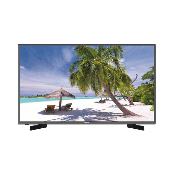
LCD TV Service Manual Back Cabinet 2.2 Specifications Hisense Confidential - 11 -... - Page 12 40LE45S 40LC45S 1920 1080 230W VideoX2 S- VideoX1 ComponentX2 HDMIX3 AV Audio X 2 Component Audio X 2 VGA Audio Input X 1 AV Audio X 1 Optical Audio out x 1 Length: 39.1 inches 12.2 inches Width: Height: 28.3 inches...
-
Page 13: Lcd Panel Spec
LCD TV Service Manual 3. LCD Panel Spec LTD42W29NUS: Panel: LTA400HA07\JK\ROH SN:1051263 3.1General Description Hisense Confidential - 12 -... -
Page 14: General Features
LCD TV Service Manual 3.2 General Features Hisense Confidential - 13 -... -
Page 15: Chassis Layout And Overall Wiring Diagrams
4.1 Boards and Chassis Layout Description Part No. Type/Model PCB/ Model Main board 120639 RSAG2.908.1375-7\ROH RSAG7.820.1525\VER.A\ROH Power board 117734 RSAG2.908.1192-11\ROH RSAG7.820.1185\VER.E\ROH AV board 113354 RSAG2.908.1232\ROH RSAG7.820.1342\VER.B\ROH keypad board 112829 RSAG2.908.1088\ROH RSAG7.820.1101\VER.B\ROH IR board 115138 RSAG2.908.1048\ROH RSAG7.820.1013\VER.A\ROH Hisense Confidential - 14 -... -
Page 16: Wires And Cables Overall Wiring Diagram(S)
Power BD XP808<--> Main BD XP5 +5V, +12V supply to Main BD TJC10T-14Y-250\ROH Main BD XP3<-->Power BD XP812 10-1 Backlight Power HX-3005B450\ROH Power BD XP809<--> Panel left backlight port Backlight Power HX-3004B550\ROH Power BD XP815<--> Panel right backlight port 10-2 Hisense Confidential - 15 -... -
Page 17: Factory/Service Osd Menu And Adjustment
For Component Video Notes: a、Press “M” button and enter factory mode. b、Press “Menu” button and enter factory OSD menu. c、Select the item “Auto Color”. d、Press VOL+ button to auto color. e、Close the OSD menu after 5 seconds. Hisense Confidential - 16 -... -
Page 18: Designer Menu
Press VOL+ button to clear the EEPROM data. c. Close the OSD menu after 5 seconds. d. Restart the TV. 5.3 Designer Menu 5.3.1 Video Mode Standard: S-Video Component HDMI R Gain G Gain B Gain Hisense Confidential - 17 -... - Page 19 G Gain B Gain 5.3.2 Video Curve: S-Video Component HDMI Bright Max Bright Min Bright Mid Contrast Contrast Min Contrast Mid Saturation Saturation Saturation Hue Max 1000 1000 1000 1000 1000 1000 Hue Min Hue Mid Hisense Confidential - 18 -...
-
Page 20: To Exit The Aging Mode
If There is a red “M” moving on the screen, it means the TV is in Aging mode. To exit the Aging mode, use your user RC, and enter 8->0->8 ->7 in sequence. The above “Factory/Service OSD Menu” are reference only, please refer to the actual units to determine the appearances. Hisense Confidential - 19 -... -
Page 21: Software Upgrading
Connect the unit to your pc with a USB-to-serial port cable. USB port connects to your pc, and serial port to the TV’s RS232 port. USB connector: to PC. Serial connector: to TV’s RS232 port. Hisense Confidential - 20 -... - Page 22 LCD TV Service Manual For the first connecting, the pc will recognize and automatically install the USB device. The process is just like the installation of a mini disk, see the following picture. Hisense Confidential - 21 -...
-
Page 23: Upgrading With The Mtktool
2—Refer to the next page instruction to select the communicate port. 3—Press the icon beside the baud rate and make sure it is green as the below picture. 4—Set the flash baud rate to 115200 as the below picture. Hisense Confidential - 22 -... - Page 24 5—Click the browse button to select the *.bin file that will be updated. 6—Click the “start” button to update software. Select mode Communicate Flash Select *.bin of Flash chip port Baud Rate file Start upgrade Information upgrade process Hisense Confidential - 23 -...
- Page 25 Note: Where or not click the “Auto Set Flash Baud Rate” in the “window” menu depends on the chip type. If the flash chip does not support high speed transport, do not select this option; otherwise, reserve the selected mood. Hisense Confidential - 24 -...
- Page 26 LCD TV Service Manual Click “Browse” button, find the upgrading program file, and select it. Press “Upgrade” button and start upgrading. The following interface appears on the screen, indicating upgrading successfully. Hisense Confidential - 25 -...
-
Page 27: Troubleshooting
Try new batteries Replace battery Replace RC Replace remote control Check IR receiver Change Led & IR board Replace Led & IR BD Change Led & IR cable Replace Led & IR cable Replace main board Hisense Confidential - 26 -... -
Page 28: Troubleshooting For Function Key
LCD TV Service Manual 7.2 Troubleshooting for Function Key Buttons does not work Replace tact switch Check switches Replace Key BD Check key board Check Key BD cable Change Key BD Replace main board Hisense Confidential - 27 -... -
Page 29: Tv Won't Power On
Check/replace IR Only BD or Keypad one works Try Power on by Check signal RC and Button OSD? Source Neither Both works Work Replace Main Replace Main BD Power on Replace Panel Replace Power BD Hisense Confidential - 28 -... -
Page 30: Troubleshooting For Audio
LCD TV Service Manual 7.4 Troubleshooting for Audio No sound Reconnect Check connecter Replace speaker wire Check speaker wire Replace speaker set Check speaker set Replace main board Replace PSU Hisense Confidential - 29 -... -
Page 31: Troubleshooting For Tv/Vga/Hdmi Input
LCD TV Service Manual 7.5 Troubleshooting for TV/VGA/HDMI input No picture on the screen Check Signal Source Make sure signal source is available Reconnect Check connect Check cable Replace cable Replace main board Hisense Confidential - 30 -... -
Page 32: Troubleshooting For Ypbpr Input
LCD TV Service Manual 7.6 Troubleshooting for YPbPr input No picture on the screen Check Source work or not Check Source Device Reconnect Check connect Check Wires (Green Blue, Red) Replace wires Replace main board Hisense Confidential - 31 -... -
Page 33: Troubleshooting For Video/S-Video Input
LCD TV Service Manual 7.7 Troubleshooting for Video/S-Video input No picture on the screen Check Source work or not Check Signal Source Reconnect Check connect Replace Cable/Wires Check Cable/ Wires Replace main board Hisense Confidential - 32 -... -
Page 34: Explode View And Explode Bom List
LCD TV Service Manual 8. Explode View and Explode Bom List 9. Schematic circuit diagram The Explode Bom list as following: ELEMENT 40LE45S PARTS LIST Part No. Description Qty. Code Number Remark 120635 Front Cover RSAG8.074.410\Z14\ROH 1047019 Button RSAG8.335.067\Z1\ROH 113354 Keypad PCA RSAG2.908.1088\ROH... - Page 35 LCD TV Service Manual 8. Explode View and Explode Bom List 9. Schematic circuit diagram The Explode Bom list as following: ELEMENT 40LE45S PARTS LIST Part No. Description Qty. Code Number Remark 120635 Front Cover RSAG8.074.410\Z14\ROH 1047019 Button RSAG8.335.067\Z1\ROH 113354 Keypad PCA RSAG2.908.1088\ROH...
- Page 37 +5VSB 2,3,4,5,6,7,8,9,10,11,12,13,14 OPWRSB OPWM1 OPWM1 +12V 2,7,8,9,14 +12V 01:INDEX/POWER IN HIGH = OFF +18V +18V +5VSB OPWRSB OPWRSB LOW = ON 02:DIGITAL/ANALOG POWER 2,6,7,8,9,11,13 +3V3SB 2,3,5,14 +3V3SB 03:MT5380PERIPHERAL +5VSB 2,9,14 +5VSB 15K/NC 15K/NC 15K/NC 15K/NC P-CH P-CH ON/OFF ON/OFF IRF7314/NC IRF7314/NC 15K/NC 15K/NC...
- Page 38 1,3,4,5,6,7,8,9,10,11,12,13,14 1,6,7,8,9,11,13 DV10 DV10 MEM_VREF MEM_VREF DV33 DDRV DDRV DV33 DV33 AV33 3,6,7,9,12 AV33 +12V 10uF/10V 10uF/10V 1,7,8,9,14 +12V AV25 100nF 100nF 6,13 AV25 AV12 AZ1117/ADJ AZ1117/ADJ 6,10,12 AV12 180R 180R +5V_TUNER 100nF 100nF +5V_TUNER 100uF/16V 100uF/16V +3V3SB 1,3,5,14 +3V3SB 100uF/16V 100uF/16V DDRV...
- Page 39 1,2,4,5,6,7,8,9,10,11,12,13,14 AV33 N12B N12B 2,6,7,9,12 AV33 DV33 DV33 OSDA0 +3V3SB 1,2,5,14 +3V3SB OSDA0 OSCL0 GPIO_0 OSDA1 OSDA1 OSCL0 GPIO_0 OSDA1 GPIO_1 OSCL1 OSCL1 OSDA1 GPIO_1 OSCL1 GPIO_3 OSDA0 9,12 OSDA0 OSCL1 GPIO_3 OPWM0 GPIO_4 +3V3SB OSCL0 9,12 OSCL0 OPWM0 GPIO_4 OPWM1 GPIO_5 +3V3SB...
- Page 40 N12A N12A 1,2,3,5,6,7,8,9,10,11,12,13,14 DDRV DDRV RDQS0 MEM_VREF RDQS0 MEM_VREF RDQM0 DDRV RDQM0 DDRV RDQ0 RWE# RDQ0 RWE_ RDQ1 RBA0 RDQ1 RBA0 RDQ2 RDQ2 RDQ3 RBA1 MEM_DQ0 MEM_DQ15 RDQ3 RBA1 DQ15 RDQ4 Add serial resistors for DRAM +1V3D RDQ4 VDDQ VSSQ RDQ5 RRAS# MEM_DQ1...
- Page 41 1,2,3,4,6,7,8,9,10,11,12,13,14 +5VSB 1,2,9,14 +5VSB N12J N12J +3V3SB 1,2,3,14 +3V3SB DV33 DV33 POCE0# U0RX DV33 POOE# DV33 DV10 DV10 POCE0_ U0RX HOLD# SCLK POOE# U0TX POCE0# DV33 DV33 PDD1 DDRV DDRV POOE_ U0TX PDD0 PDD0 DV33 +3V3SB 1,2,3,14 +3V3SB PDD0 HOLD_ PDD1 OIRI FRESET#...
- Page 42 N12D N12D USB_VRT 1,2,3,4,5,7,8,9,10,11,12,13,14 AV12 2,10,12 AV12 USB_VRT AVDD12_PLL 5K1 1% 5K1 1% C114 C114 USB_VRT AVDD12_ADCPLL 1,2,7,8,9,11,13 USB_DM AVDD12_PLL AV33 USB_DM AVDD12_TVDPLL 2,3,7,9,12 AV33 100pF/NC 100pF/NC USB_DP AVDD12_PLL AV25 USB_DP AVDD12_HDMIPLL 2,13 AV25 AVDD33_USB AVDD12_PLL AV12 ADIN3 AVDD33_USB AVDD12_APLL ADIN3 AVDD12_USB AVDD12_PLL...
- Page 43 1,2,3,4,5,6,8,9,10,11,12,13,14 OFF_MUTE OFF_MUTE AL1O R121 R121 AL1O N12G N12G SPDIF_OUT AR1O AR1O ADAC_VCM 470R 470R AIN0_L SPDIF_OUT SPDIF_OUT AIN0_L ASPDIF AIN0_R AOMCLK YPBPR0L_IN TP10 TP10 C140 C140 YPBPR0L_IN AIN0_R AOMCLK AV33 AIN1_L AOLRCK YPBPR0R_IN C141 C141 YPBPR0R_IN AIN1_L AOLRCK REFP_AADC VIMD_AADC 10uF/10V 10uF/10V...
- Page 44 +12V 1,2,3,4,5,6,7,9,10,11,12,13,14 CE46 220uF/16V CE46 220uF/16V VREG 1,2,6,7,9,11,13 R164 R164 +18V +18V 1N4148 1N4148 +12V R163 R163 CPU_MUTE: HIGH FOR MUTE 1,2,7,9,14 +12V R162 R162 R165 R165 AL1_3100 AL1_3100 0R0/NC 0R0/NC 100K 100K AR1_3100 1N4148 1N4148 AR1_3100 HPDET# P_MUTE: LOW FOR MUTE SHUTDOWN MUTE_3100 MUTE_3100...
- Page 45 1,2,3,4,5,6,7,8,10,11,12,13,14 N12C N12C +5VSB 1,2,6,7,8,11,13 +5VSB +12V 1,2,7,8,14 +12V AVDD33_LVDS AVDD33_LVDSA 1,2,6,7,8,11,13 AVDD33_LVDS GPIO_4 AVDD33_LVDSB GPIO_4 AVDD33_LVDS GPIO_9 GPIO_9 AVDD33_LVDSC U2TX U2TX AVDD33_VPLL U2RX AVDD33_VPLL U2RX DV33 DV33 CK1N AV33 2,3,6,7,12 AV33 CK1N CK1P CK1P TP13 TP13 LVDSVDD LVDSVDD HPOUTL TP12 TP12 HPOUTL...
- Page 46 1,2,3,4,5,6,7,8,9,11,12,13,14 HSYNC HSYNC AV12 VSYNC VSYNC N12E N12E AVDD12_RGBADC SOY0 DVDD12_VGA AV12 120R 120R SOY0 DVDD12_VGA AVSS12_RGBADC C221 C221 AVSS12_RGBADC AVDD12_RGBADC C222 C222 DVDD12_VGA AVDD12_RGBADC PB0P AVSS12_RGBFE 120R 120R PB0P AVSS12_RGBFE 100nF 100nF PBR0N AVDD12_RGBFE PBR0N AVDD12_RGBFE PR0P AVSS12_RGBADC C223 C223 AV12 C224...
- Page 47 1,2,3,4,5,6,7,8,9,10,12,13,14 +5VSB 1,2,9,14 +5VSB VSYNC VSYNC HSYNC HSYNC VGAR_IN VGAR_IN VGAL_IN VGAL_IN U0RX U0RX U0TX U0TX GPIO_6 GPIO_6 NEARLY IC U0TX NEARLY VGA CON. U0TX U0RX U0RX R231 R231 C245 C245 4.7nF 4.7nF 1,2,6,7,8,9,13 R232 R232 RED_GND 100R/NC 100R/NC R233 R233 C246 C246...
- Page 48 AV33 N12K N12K AVDD33_H 1,2,3,4,5,6,7,8,9,10,11,13,14 120R 120R 1,2,6,7,8,9,11,13 RXCB AV33 TP16 TP16 2,3,6,7,9 AV33 RX0_CB EXT_RES C261 C261 OPWR0_5V C260 C260 C262 C262 AV12 2,6,10 AV12 RX0_C OPWR0_5V 4.7uF/10V 4.7uF/10V RX0B AV25 100nF 100nF 2,6,13 AV25 RX0_0B GPIO_8 GPIO_8 RX0_0 RX1B GPIO_1 GPIO_1...
- Page 49 1,2,3,4,5,6,7,8,9,10,11,12,14 AV25 AV25 AVLIN_SW N12F N12F AVLIN_SW AVRIN_SW AVRIN_SW CVBS0T AV25 CVBS0T CVBS0 DVDD25_VADC 1,2,6,7,8,9,11 CVBS0 DVDD25_VADC AV25 Near chip CVBS1 DVSS25_VADC SPDIF_OUT SPDIF_OUT CVBS1 DVSS25_VADC GND_TUNER C279 C279 CVBS0T DVDD25_VADC AVDD25_REF CVBS0T GND_TUNER GND_CVBS FAT_IN2+ VIP_ATV CVBS1T GD_CVBS 120R 120R CVBS1T 120R...
- Page 50 1,2,3,4,5,6,7,8,9,10,11,12,13 +3V3SB 1,2,3,5 +3V3SB +5VSB 1,2,9 +5VSB +12V 1,2,7,8,9 +12V 1,2,6,7,8,9,11,13 DV33 2,3,5 DV33 OPCTRL1 OPCTRL1 OIRI OIRI AR1O AR1O AL1O AL1O ADIN1 ADIN1 ADIN2 ADIN2 +5VSB 1,2,9 +5VSB AR1_3100 AR1_3100 AL1_3100 AL1_3100 R350 R350 C319 C319 +3V3SB 100pF 100pF CE57 CE57 R353...
Need help?
Do you have a question about the 40LE45S and is the answer not in the manual?
Questions and answers