Table of Contents
Advertisement
Service
Manual
MULTI-COMPACT DISC PLAYER
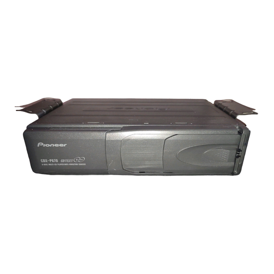
CDX-P670
- This service manual should be used together with the following manual(s):
Model No.
Order No.
CX-892
CRT2356
CONTENTS
1. SAFETY INFORMATION ............................................3
2. EXPLODED VIEWS AND PARTS LIST .......................4
4. PCB CONNECTION DIAGRAM ................................22
5. ELECTRICAL PARTS LIST ........................................28
6. ADJUSTMENT..........................................................31
PIONEER CORPORATION
PIONEER ELECTRONICS SERVICE INC.
PIONEER EUROPE NV
Haven 1087 Keetberglaan 1, 9120 Melsele, Belgium
PIONEER ELECTRONICS ASIACENTRE PTE.LTD. 253 Alexandra Road, #04-01, Singapore 159936
C PIONEER CORPORATION 2000
Mech. Module
Remarks
C7
CD Mech. Module:Circuit Description, Mech. Description, Disassembly
4-1, Meguro 1-Chome, Meguro-ku, Tokyo 153-8654, Japan
P.O.Box 1760, Long Beach, CA 90801-1760 U.S.A.
7. GENERAL INFORMATION .......................................38
7.1 DIAGNOSIS ........................................................38
7.1.1 TEST MODE ..............................................38
7.1.2 DISASSEMBLY .........................................44
7.2 IC .........................................................................47
7.3 OPERATIONAL FLOW CHART ...........................49
8. OPERATIONS AND SPECIFICATIONS.....................50
K-ZZY. NOV. 2000 Printed in Japan
ORDER NO.
CRT2589
X1N/EW
Advertisement
Table of Contents

Related Manuals for Pioneer CDX-P670X1N


Summary of Contents for Pioneer CDX-P670X1N
-
Page 1: Table Of Contents
PIONEER ELECTRONICS SERVICE INC. P.O.Box 1760, Long Beach, CA 90801-1760 U.S.A. PIONEER EUROPE NV Haven 1087 Keetberglaan 1, 9120 Melsele, Belgium PIONEER ELECTRONICS ASIACENTRE PTE.LTD. 253 Alexandra Road, #04-01, Singapore 159936 C PIONEER CORPORATION 2000 K-ZZY. NOV. 2000 Printed in Japan... - Page 2 CDX-P670 - CD Player Service Precautions 2. During disassembly, be sure to turn the power off since an internal IC might be destroyed when a con- 1. For pickup unit(CXX1285) handling, please refer nector is plugged or unplugged. to"Disassembly"(see page 44). 3.
-
Page 3: Safety Information
CDX-P670 1. SAFETY INFORMATION 1. Safety Precautions for those who Service this Unit. • When checking or adjusting the emitting power of the laser diode exercise caution in order to get safe, reliable results. Caution: 1. During repair or tests, minimum distance of 13cm from the focus lens must be kept. 2. -
Page 4: Exploded Views And Parts List
CDX-P670 2. EXPLODED VIEWS AND PARTS LIST 2.1 PACKING... - Page 5 CDX-P670 NOTE: - Parts marked by “*”are generally unavailable because they are not in our Master Spare Parts List. ∇ mark on the product are used for disassembly. - Screws adjacent to - PACKING SECTION PARTS LIST Mark No. Description Part No.
- Page 6 CDX-P670 2.2 EXTERIOR...
- Page 7 CDX-P670 - EXTERIOR SECTION PARTS LIST Mark No. Description Part No. 1 Screw BMZ26P040FMC 2 Screw BMZ30P040FZK 3 Button CAC6363 4 Screw CBA1460 5 Spring CBH1859 6 Connector CDE5525 7 Connector CDE6478 8 Upper Case CNB2431 9 Arm CNC8058 10 Insulator CNM6074 11 Panel CNS5216...
- Page 8 CDX-P670 2.3 CD MECHANISM MODULE...
- Page 9 CDX-P670 - CD MECHANISM MODULE SECTION PARTS LIST Mark No. Description Part No. Mark No. Description Part No. 1 Connector CDE6069 46 Spacer CNM6428 2 CD Core Unit CWX2487 47 Sheet CNM6296 3 Connector(CN701) CKS1963 48 PCB CNP5227 4 Connector(CN101) CKS2272 49 PCB CNP5228...
- Page 10 CDX-P670 Mark No. Description Part No. 91 Screw JGZ17P025FZK 92 Pickup Unit(Service) CXX1285 93 ••••• 94 ••••• 95 Screw IMS26P040FMC 96 Screw JFZ20P025FNI 97 Photo-transistor(Q851) PT4800 CSN1051 Spring Switch(S851,S853) 99 LED(D851) CN504-2 100 Spring Switch(S852) CSN1052...
- Page 11 CDX-P670 2.4 MAGAZINE ASSY - MAGAZINE ASSY SECTION PARTS LIST Mark No. Description Part No. 1 Magazine Assy CXB6518 2 Label CRW1415 3 Tray CNV5341...
-
Page 12: Block Diagram And Schematic Diagram
CDX-P670 3. BLOCK DIAGRAM AND SCHEMATIC DIAGRAM 3.1 BLOCK DIAGRAM MECHANISM CD CORE UNIT PICKUP UNIT (SERVICE) (P8) CN101 L_OUT MONITOR DIODE RF AMP, SERVO, DSP, DAC AC/F/E/BD HOLOGRAM IC 201 UNIT UPD63711GC LIMIT CDMUTE xtal Q101 X202 16.93MHz LD(–) XTAL LASER IPIN... - Page 13 CDX-P670 POWER UNIT CN921 CN701 CN911 LOUT LOUT IP-BUS OUT Q941 Q942 CDMUTE CDMUTE CDMUTE IP-BUS DRIVER BUSP BUSP IC 703 IPIN BUSM BUSM HA12187FP IPOUT ASENB IPPW BATT BSENIN BSENIN bsens IC 704 ASENB ASNB asens PAJ002A reset Q770 RESET SW S802 Q771...
-
Page 14: Cd Mechanism Module
CDX-P670 3.2 CD MECHANISM MODULE Note: When ordering service parts, be sure to refer to “EXPLODED VIEWS AND PARTS LIST” or “ELECTRICAL PARTS LIST”. MECHANISM PICKUP UNIT(SERVICE) CXX1285 RF AMP, SE M854 CXB3004 M851 CXB3003 SWITCH PCB CSN1051 CN504-2 PT4800 CSN1052 CSN1051 M853... - Page 15 CDX-P670 NOTE : Symbol indicates a resistor. Decimal points for resistor No differentiation is made between chip resistors and and capacitor fixed values discrete resistors. are expressed as : ← Symbol indicates a capacitor. ← No differentiation is made between chip capacitors and 0.022 R022 discrete capacitors.
- Page 16 CDX-P670 SYSTEM CONTROLLER...
- Page 17 CDX-P670 SRAM IP-BUS DRIVER...
- Page 18 CDX-P670 Note:1. The encircled numbers denote measuring pointes in the circuit diagram. 2. Reference voltage REFO:2.5V - Waveforms 1 RFI 1 CH1: RFI 1 CH1: RFI 0.5V/div. 0.5µs/div. 1V/div. 1V/div. 0.5ms/div. 0.5ms/div. 2 CH2: MIRR 2 CH2: MIRR Normal mode: play 5V/div.
- Page 19 CDX-P670 8 CH1: TE 0 MD 8 CH1: TE 0.2V/div. 0.5V/div. 0.5V/div. 0.1s/div. 5ms/div. 20ms/div. 9 CH2: TD ! CH2: SD 0.2V/div. 0.5V/div. Normal mode: play TEST mode:100Tracks jump(FWD) Normal mode: Play (12cm) → REFO → REFO → REFO → →...
- Page 20 CDX-P670 ( CH1: R OUT 8 CH1: TE 6 CH1: FE 2V/div. 0.2V/div. 0.2V/div. 1ms/div. 500µs/div. 1ms/div. ) CH2: L OUT 3 CH2: FD 9 CH2: TD 2V/div. 0.5V/div. 0.5V/div. Normal mode: Play (1kHz 0dB) Normal mode: During AGC Normal mode: During AGC →...
- Page 21 CDX-P670 3.3 POWER UNIT...
-
Page 22: Pcb Connection Diagram
CDX-P670 4. PCB CONNECTION DIAGRAM SIDE A 4.1 CD CORE UNIT M852 NOTE FOR PCB DIAGRAMS 1. The parts mounted on this PCB include all necessary parts for several destination. For further information for respective destinations, be sure to check with the schematic dia- gram. - Page 23 CDX-P670 SIDE B...
- Page 24 CDX-P670 4.2 POWER UNIT SIDE A POWER UNIT CN701 IP-BUS CORD...
- Page 25 CDX-P670 SIDE B POWER UNIT...
- Page 26 CDX-P670 4.3 MECHANISM PCB MECHANISM PCB PICKUP UNIT M851 (SERVICE) SPDL HOME M854 CN101 4.4 SWITCH PCB SWITCH PCB D851...
- Page 27 CDX-P670 4.5 MOTOR PCB MOTOR PCB...
-
Page 28: Electrical Parts List
CDX-P670 5. ELECTRICAL PARTS LIST NOTE: - Parts whose parts numbers are omitted are subject to being not supplied. - The part numbers shown below indicate chip components. Chip Resistor RS1/_S___J,RS1/__S___J Chip Capacitor (except for CQS..) CKS.., CCS.., CSZS..=====Circuit Symbol and No.===Part Name Part No. - Page 29 CDX-P670 =====Circuit Symbol and No.===Part Name Part No. =====Circuit Symbol and No.===Part Name Part No. ------ ------------------------------------------ ------------------------- ------ ------------------------------------------ ------------------------- RS1/10S221J Unit Number : CWX2512 RS1/10S271J Unit Name : Power Unit RS1/16S562J RS1/16S562J MISCELLANEOUS RS1/16S102J Transistor 2SD2396 CAPACITORS Transistor IMD2A Transistor IMX1...
- Page 30 CDX-P670 =====Circuit Symbol and No.===Part Name Part No. ------ ------------------------------------------ ------------------------- Unit Number Unit Name : Motor PCB Motor Unit(TRAY) CXB4421 Miscellaneous Parts List Pickup Unit(P8)(Service) CXX1285 Motor Unit(SPINDLE) CXB3003 Motor Unit(ELV) CXB3006 Motor Unit(CARRIAGE) CXB3004 Volume 10kΩ(B) CCW1023...
-
Page 31: Adjustment
CDX-P670 6. ADJUSTMENT 6.1 CD ADJUSTMENT - Precautions • Disc detection during tray extraction and return oper- • This unit uses a single power supply (+5V) for the reg- ations is performed by means of the photo transistor ulator. The signal reference potential, therefore, is in this unit. - Page 32 CDX-P670 6.2 CHECKING THE GRATING - Checking the Grating After Changing the Pickup Unit • Note : CD mechanism modules the grating angle of the pickup unit cannot be adjusted after the pickup unit is changed. The pickup unit in the CD mechanism module is adjusted on the production line to match the CD mechanism module and is thus the best adjusted pickup unit for the CD mechanism module.
- Page 33 CDX-P670 Grating waveform Echt Xch 20mV/div, AC Fcht Ych 20mV/div, AC 0˚ 30˚ 45˚ 60˚ 75˚ 90˚...
- Page 34 CDX-P670 6.3 ADJUSTMENT OF ELEVATION WHEN THE CD CORE UNIT HAS BEEN REMOVED FOR MAINTENANCE - Adjustment When Error Code 60 is Displayed Because of Malfunctioning Elevation • Note : This mechanisms is detects the height of the stage using slide-variable resistance. To absorb dislocation of the stage height caused by differences in the mechanism and the CD core unit, adjustment must be made for each CD-mechanism module using a variable resistor.
- Page 35 CDX-P670 Examples of display 4. Press key 9 to set ELV/TRAY mode to TRAY. TRACK FUNCTION 01' 02" 5. Press key FF to release the clamp and return the tray to the magazine. Release the clamp 6. Press key 9 to enter Elevation Move mode. TRACK FUNCTION 00' 02"...
- Page 36 CDX-P670 12. To see the amount of dislocation, place the mechanism upside-down. If the stopper bend has been dislocated in the direction of the first CD, turn VR802 to the left(Fig. 2). VR802 EREF To lower the stage toward the sixth step by 0.1 mm, reduce the volt- age of EREF (adjusted in step 8) by 20 mV.
- Page 37 CDX-P670 Stopper bend of the clamp lever Frame stopper Dislocated toward the first CD. Fig. 2 Adjust the insertion gate of magazine to the third scale. Fig. 1 Engaged in the center and pressed downward. Fig. 3 Dislocated toward the sixth CD. Fig.
-
Page 38: General Information
CDX-P670 7. GENERAL INFORMATION 7.1 DIAGNOSIS 7.1.1 TEST MODE - CD Test mode • The following head units are exceptional so that their This mode is used for adjusting the CD mechanism entering ways to the test mode are different from oth- module of the device. - Page 39 CDX-P670 - Flow Chart Test Mode In Reset SOURCE Sourse CD New test mode BAND Power ON (Adjustment for T.Offset) Power ON RF AMP Gain Select (Not adjustment for T.Offset) 00 00 00 Display 99 99 99 GG GG GG Display Power OFF TRK+...
- Page 40 CDX-P670 - Error Messages If a CD is not operative or stopped during operation due to an error, the error mode is turned on and cause(s) of the error is indicated with a corresponding number. This arrangement is intended at reducing nonsense calls from the users and also for facilitating trouble analysis and repair work in servicing.
- Page 41 CDX-P670 Code Class Displayed error code Description of the code and potential cause(s) Mecha- An error upon Elevation time has time out. nism elevation Mecha- An error with an em- No disc is available. nism pty magazine inserted Remarks: Unreadable TOC does not constitute an error. An intended operation continues in this case. A newly designed head unit must conform to the example given above.
- Page 42 CDX-P670 Mechanism Test Mode (Example) BAND Back to the test mode Playing the mechanism DOWN Playing the mechanism Mechanism test mode in – TRAY/ELV select – – Operation step select Note: Eject and CD on/off is performed in the same procedure as that for the normal mode. (3) Cause of Error and Error Code Code Class Contents...
- Page 43 CDX-P670 Status No. Contents Protective action Focus search preprocessing is in None progress while focus recovery is turned on. Wait time after focus close is set up. Off focus. Standing by after focus close is over. Off focus. Setup (1/2) before T balance adjustment is started. Off focus.
-
Page 44: Disassembly
CDX-P670 7.1.2 DISASSEMBLY Removing the Upper Case (not shown) 1. Remove the nine screws. 2. Remove the Upper Case. CD Mechanism Module Removing the CD Mechanism Module (Fig.5) Remove the four dampers. Remove the two springs. Disconnect the connector and then remove the CD Mechanism Module. - Page 45 CDX-P670 Door(A) 2. The slide is done in the direction of arrow5 and remove the Door(B) while spread out the Door(A) in the Door(B) direction of arrow4. (Fig.8) *) The illustration of the text for 12-Disc type but disas- sembling method is the same for 6-Disc type. Fig.8 - Removing the Pickup Unit 1.
-
Page 46: Connector Function Description46
CDX-P670 7.1.3 CONNECTOR FUNCTION DESCRIPTION IP-BUS POWER SUPPLY 8 9 10 11 1 2 3 4 1.GND 7.LCH 1.BUS+ 2.ACC 8.ASENB 2.GND 3.BATT 3.GND 9.RCH 4.NC 10.SGNDR 11.SGNDL 5.BUS- 6.GND... - Page 47 CDX-P670 7.2. IC - Pin Functions (PD5638A) Pin No. Pin Name Format Function and Operation Not used adena A/D reference voltage output TXTSTB TEXT parameter output TXTSO TEXT control parameter serial output TXTSI TEXT data serial input TXTSCK TEXT clock output BYTE VCC joint CNVSS...
- Page 48 CDX-P670 Pin No. Pin Name Format Function and Operation 65–68 A6-A3 SRAM address bus output SRAM address bus output A2 & (EPSK) SRAM address bus output and (E2PROM clock output) A1 & (EPDI) SRAM address bus output and (E2PROM data input) A0 &...
-
Page 49: Operational Flow Chart
CDX-P670 7.3 OPERATIONAL FLOW CHART BATT ON VDD=5V Pin16 bsens Pin18 bsens=L POWER←H Pin10 adena←L Pin3 VD IN Error message "A0" Pin96 1.3V VD IN 2.1V POWER←L Pin75 Stand-by mag=L DISC Search POWER←L Pin10 asens Pin19 asens=L Source=Multi-CD POWER←H Pin10 adena←L Pin3 VD IN Error message "A0"... -
Page 50: Operations And Specifications
CDX-P670 8. OPERATIONS AND SPECIFICATIONS 8.1 OPERATIONS Connecting the Units IP-BUS cable To prevent incorrect connection, the input side of the IP-BUS connector is colored in blue, and the output side in black. Connect the connectors of the same colors correctly. IP-BUS output (black) Connect the black connector of the cable to this 600 cm...
Need help?
Do you have a question about the CDX-P670X1N and is the answer not in the manual?
Questions and answers