Sony MV-900SDS Service Manual
Mobile dvd system
Hide thumbs
Also See for MV-900SDS:
- Operating instructions manual (96 pages) ,
- Limited warranty (1 page) ,
- Specifications (2 pages)
Table of Contents
Advertisement
SERVICE MANUAL
Ver. 1.4 2006.08
COMPONENT MODEL NAME
DVD PLAYER
CORDLESS STEREO HEADPHONES
CARD REMOTE COMMANDER
Note: There are two types of Cordless Stereo Headphones. For further information, see "NOTE WHEN
REPLACING THE CORDLESS STEREO HEADPHONES" (page 3) of the Servicing Notes.
Copyrights
This product incorporates copyright protection
technology that is protected by method claims
of certain U.S. patents, other intellectual
property rights owned by Macrovision
Corporation, and other rights owners. Use of
this copyright protection technology must be
authorized by Macrovision Corporation, and is
intended for home and other limited viewing
uses only unless otherwise authorized by
Macrovision Corporation. Reverse engineering
or disassembly is prohibited.
• "Memory Stick,"
and "MagicGate
Memory Stick" are trademarks of Sony
Corporation.
• "Memory Stick Duo" and "
are trademarks of Sony Corporation.
• "MagicGate" and "
trademarks of Sony Corporation.
• "Memory Stick PRO" and "
are trademarks of Sony Corporation.
Manufactured under license from Dolby
Laboratories. "Dolby", "Pro Logic", and the
double-D symbol are trademarks of Dolby
Laboratories.
"DTS," "DTS Digital Surround" and "DTS
Digital Out" are trademarks of Digital Theater
Systems, Inc.
Sony Corporation
9-877-871-05
eVehicle Division
2006H05-1
Published by Sony Techno Create Corporation
© 2006.08
MODEL NUMBER LABEL
MV-900SDS
MDR-IF0140
MV-01HP
–
DVD player XVM-R90D
System
Laser
Signal format system
Audio characteristics
Frequency response
Signal to noise ratio
Harmonic distortion
Dynamic range
Wow and flutter
"
" are
General
"
Outputs
Inputs
Power requirements
Dimensions
Mass
Operating temperature
MV-900SDS
PRINTED MODEL NAME
XVM-R90D
MDR-IF0140
MV-01HP
RM-X137
SPECIFICATIONS
Semiconductor laser
NTSC/PAL
20 Hz to 20 kHz
90 dB (A)
0.05 %
90 dB
below measurable limits
(±0.001% W PEAK)
FM output
Audio output
Video output
Optical output
Audio input
Video input
DC 12V input
12 V DC
Approx. 285 × 73 × 455 mm
× 2
× 18 in)
(11
1
/
7
/
4
8
(w/h/d)
Approx. 3.5 kg
(7 lb 12 oz)
0 °C to 45 °C
(32 °F to 113 °F)
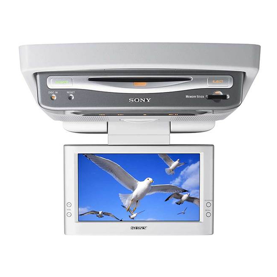
MOBILE DVD SYSTEM
US Model
Supplied accessories
Card remote commander
RM-X137
Power supply cord (1)
RF modulator cable (1)
Mounting plate (1)
Screws (5)
Tapping screws (8)
Operating Instructions (1)
Monitor
System
Liquid crystal color display
Display
Manual flipdown panel
Drive system
TFT-LCD active matrix
system
Picture size
9 inches wide screen (16:9)
336,960 (w 1,440 × h 234)
Picture segment
dots
Cordless Stereo Headphones
MDR-IF0140
General
Modulation system
Frequency modulation
Carrier frequency
Right 2.8 MHz
Left 2.3 MHz
18 − 22,000 Hz
Frequency response
Power source
DC 1.5 V (size AAA) dry
battery
Mass
Approx. 125 g (4.41 oz)
including battery
5 °C to 35 °C
Operating temperature
(41 °F to 95 °F)
Design and specifications are subject to change
without notice.
Advertisement
Chapters
Table of Contents

Related Manuals for Sony MV-900SDS


Summary of Contents for Sony MV-900SDS
-
Page 1: Specifications
System Liquid crystal color display • “Memory Stick,” and “MagicGate Harmonic distortion 0.05 % Display Manual flipdown panel Memory Stick” are trademarks of Sony Drive system TFT-LCD active matrix Dynamic range 90 dB Wow and flutter below measurable limits system Corporation. -
Page 2: Table Of Contents
MV-900SDS TABLE OF CONTENTS CAUTION The use of optical instruments with this SERVICING NOTES ..........3 product will increase eye hazard. GENERAL Location of Controls ............5 CAUTION Use of controls or adjustments or performance of procedures DISASSEMBLY other than those specified herein may result in hazardous radiation 3-1. -
Page 3: Servicing Notes
MV-900SDS Ver. 1.4 SECTION 1 SERVICING NOTES UNLEADED SOLDER NOTES ON HANDLING THE OPTICAL PICK-UP Boards requiring use of unleaded solder are printed with the lead- BLOCK OR BASE UNIT free mark (LF) indicating the solder contains no lead. The laser diode in the optical pick-up block may suffer electrostatic... - Page 4 MV-900SDS Region code of DVDs this player About discs this player can can play This player has a region code printed on the play rear of the player and will only play DVDs that are labeled with identical region codes. DVDs...
-
Page 5: General
MV-900SDS SECTION 2 This section is extracted from instruction manual. GENERAL Location of controls XVM-R90D Refer to the pages listed for details. 1 Disc slot q; “Memory Stick” slot 2 POWER (on/off) button qa x (stop) button To turn on/off the player. - Page 6 MV-900SDS Card remote commander RM-X137 The corresponding buttons of the card remote commander control the same DISPLAY POWER functions as those on the player. Instructions in this manual describe how to use SEARCH the player by mainly using the card remote CLEAR commander.
- Page 7 Cordless Stereo Headphones MDR-IF0140 Battery life Size AAA dry battery (1) is supplied with the headphones. Battery Approx. hours* Sony alkaline battery 60 hours* LR03/AM-4 (N) Sony manganese battery 28 hours* R03/UM-4 (NU) at 1 kHz, 1 mW+1 mW output Time stated above may vary, depending on the temperature or conditions of use.
-
Page 8: Connection Diagram
— in a place to subject to temperature extremes (below 5˚C (41˚F) or above 35˚C (95˚F)). Refer to the operating instructions supplied to PS one™. “PS one” is a trademark of Sony Computer Entertainment Inc. Connection diagram Refer to the connection diagram for the proper connections. -
Page 9: Disassembly
MV-900SDS SECTION 3 DISASSEMBLY • This set can be disassembled in the order shown below. 3-1. DISASSEMBLY FLOW 3-2. BRACKET (MAIN) 3-5. REAR COVER (HINGE) (Page 9) (Page 11) 3-3. DVD MECHANISM 3-4. MAIN BOARD 3-6. LCD BLOCK DECK BLOCK... -
Page 10: Dvd Mechanism Deck Block
MV-900SDS 3-3. DVD MECHANISM DECK BLOCK 2 two screws × (BTP2.6 3 two screws × (BTP2.6 4 bracket (front) 5 two screws × (BTP2.6 6 DVD mechanism deck block 1 flexible flat cable (50P) (CN101) 3-4. MAIN BOARD 2 connector (CN108) 3 screw ×... -
Page 11: Rear Cover (Hinge)
MV-900SDS 3-5. REAR COVER (HINGE) LCD block 3 two claws 4 rear cover (hinge) 2 two screws × 1 Slide the knob (open) in the direction of arrow A , and open the LCD block in the direction of arrow B . -
Page 12: Lcd Board
MV-900SDS 3-7. LCD BOARD 4 two connectors 1 four screws × (CN906, 907) 6 screw × (PS2.6 5 eight screws × (BTP2 4 connector 2 rear case (LCD) (CN850) 4 two connectors (CN905, 908) 7 LCD board 3 flexible board (CN801) 3-8. -
Page 13: Test Mode
MV-900SDS SECTION 4 TEST MODE Note: This set is able to setting the adjustment data, reset to factory default 3. LCD SETTING and initialize the EEPROM (IC402 on the MONITOR board) in the This mode is not used in servicing. -
Page 14: Electrical Adjustments
MV-900SDS SECTION 5 ELECTRICAL ADJUSTMENTS 1. DC/DC CONVERTER ADJUSTMENT 2. PLL ADJUSTMENT 1-1. Frequency Adjustment Setting: Setting: digital voltmeter oscilloscope MONITOR board frequency counter TP601 MONITOR board TP602 – TP802 Procedure: TP804 – 1. Connect a digital voltmeter to the TP601 and TP602 on the MONITOR board. - Page 15 MV-900SDS 5. NTSC SUB CARRIER CHECK – Waveform Position Set-up Adjustment – 7. Adjust the RV802 on the MONITOR board so that A value Setting: of waveform becomes –1.7 V ±0.1 V. frequency counter MONITOR board 4.6 V ± 0.1 V TP510 A : –...
- Page 16 MV-900SDS 2 Back Limiter Level 8 Gamma 1 Procedure: Procedure: 1. In the “1 Contrast Level of Luminance Signal” status, press 1. In the “7 B-ch Sub Contrast” status, connect the oscilloscope the [MENU] utton to display “Black Limit”, and press the to the TP513 and TP811 on the MONITOR board.
- Page 17 MV-900SDS Adjustment Location: – LCD BOARD (Side A) – TP853 RV601 RV803 RV801 RV802 – LCD BOARD (Side B) – TP811 TP810 TP828 TP812 TP819 TP506 TP832 TP806 TP802 TP601 TP807 TP510 TP602 TP808 TP513 TP405 TP804 TP805 TP987 TP854...
- Page 18 MV-900SDS MEMO...
-
Page 19: Diagrams
MV-900SDS SECTION 6 DIAGRAMS 6-1. BLOCK DIAGRAM – MPEG DECODER Section – B+8V B+5V • R-ch is omitted due to same as L-ch. CVBS, Y, B-Y, R-Y CVBS • SIGNAL PATH (Page 21) : DVD (VIDEO) : DVD (AUDIO) HDO – HD15 HD0 –... -
Page 20: Block Diagram - Audio Section
MV-900SDS 6-2. BLOCK DIAGRAM – AUDIO Section – RV900 • R-ch is omitted due to same as L-ch. IR TRANSMITTER LED DRIVE D912, 914, 916 MODULATOR Q902 (IR TRANSMITTER) • SIGNAL PATH IC904 : DVD (AUDIO) : AUX INPUT (AUDIO) -
Page 21: Block Diagram - Video, Panel Section
MV-900SDS 6-3. BLOCK DIAGRAM – VIDEO, PANEL Section – VIDEO INPUT SELECT IC101 J701 (2/2) VIDEO 6 VIN1 INPUT J702 (2/2) VIDEO VOUT OUTPUT CVBS, Y, LIQUID CRYSTAL B-Y, R-Y CVBS 4 VIN2 DISPLAY MODULE TRAP RV802 LCD1 (Page 19) -
Page 22: Block Diagram - Power Supply Section
MV-900SDS 6-4. BLOCK DIAGRAM – POWER SUPPLY Section – BATT +12V M301 B+SWITCH REGULATOR (FAN) Q307, 308 IC302 FAN CONT SW12V B+SWITCH IR LED B+ Q904, 905 IR CONT D903 DISC SLOT IR +8V REGULATOR DC/DC ILLUMINATION IC903 CONVERTER T801... -
Page 23: Main Board (Component Side)
MV-900SDS • Note for Printed Wiring Boards and Schematic Diagrams • Circuit Boards Location Note on Printed Wiring Boards: Note on Schematic Diagram: • X : parts extracted from the component side. • All capacitors are in µF unless otherwise noted. (p: pF) JACK (OUT) board •... -
Page 24: Printed Wiring Board Main Board (Component Side)
MV-900SDS • See page 23 for Circuit Boards Location. 6-5. PRINTED WIRING BOARD – MAIN Board (Component Side) – : Uses unleaded solder. Ver 1.1 • Semiconductor Location (Page 30) (Page 30) (Page 30) (Page 30) (Page 37) Ref. No. Location... -
Page 25: Printed Wiring Board - Main Board (Conductor Side)
MV-900SDS • See page 23 for Circuit Boards Location. 6-6. PRINTED WIRING BOARD – MAIN Board (Conductor Side) – : Uses unleaded solder. J301 OPTICAL OUTPUT MAIN BOARD (CONDUCTOR SIDE) Q315 D309 R337 E C B Q325 B C E... -
Page 26: Schematic Diagram - Main Board (1/4)
MV-900SDS Ver 1.1 • See page 39 for Waveforms. • See page 47 for IC Pin Function Description. 6-7. SCHEMATIC DIAGRAM – MAIN Board (1/4) – CN102 (1/4) BS AUX5 C104 MS BS SDIO C103 MS SDIO C102 MS INS 4.7k... -
Page 27: Schematic Diagram - Main Board (2/4)
MV-900SDS • See page 39 for Waveforms. • See page 41 for IC Block Diagrams. 6-8. SCHEMATIC DIAGRAM – MAIN Board (2/4) – (Page 26) (2/4) RB491D-T146 RB25 4.7k 0.022 FLASH ROM RESET SIGNAL GENERATOR MBM29LV800TA -70PFTN PST3645NR MA8068-L-TX 1000p... -
Page 28: Schematic Diagram - Main Board (3/4)
MV-900SDS • See page 38 for Waveforms. • See page 41 for IC Block Diagrams. 6-9. SCHEMATIC DIAGRAM – MAIN Board (3/4) – C212 (3/4) C217 R209 R212 Q201-204 C215 C213 1000p 0.01 RF LEVEL C214 R232 C201 R207 SWITCHING... -
Page 29: Schematic Diagram - Main Board (4/4)
MV-900SDS • See page 41 for IC Block Diagrams. 6-10. SCHEMATIC DIAGRAM – MAIN Board (4/4) – (4/4) C755 C756 C757 C750 R776 C758 C762 C764 CN705 1000 10V 1000 10V D701 1SS133 R762 C744 R766 R768 R770 C748 C752 (L-CH) 4.7k... -
Page 30: Printed Wiring Board - Lcd Board (Side A)
MV-900SDS • See page 23 for Circuit Boards Location. 6-11. PRINTED WIRING BOARD – LCD Board (Side A) – : Uses unleaded solder. LCD BOARD (SIDE A) (Page 24) (Page 24) (Page 24) (Page 24) MAIN MAIN MAIN MAIN BOARD... -
Page 31: Printed Wiring Board - Lcd Board (Side B)
MV-900SDS • See page 23 for Circuit Boards Location. 6-12. PRINTED WIRING BOARD – LCD Board (Side B) – : Uses unleaded solder. LCD BOARD (SIDE B) R877 C404 R876 Q861 R454 R453 R428 R478 R871 C450 R458 R875 R855... -
Page 32: Schematic Diagram - Lcd Board (1/4)
MV-900SDS • See page 39 for Waveforms. • See page 41 for IC Block Diagrams. • See page 47 for IC Pin Function Description. 6-13. SCHEMATIC DIAGRAM – LCD Board (1/4) – (1/4) R519 R520 4.7k 4.7k D501 R521 R524... -
Page 33: Schematic Diagram - Lcd Board (2/4)
MV-900SDS • See page 39 for Waveforms. • See page 41 for IC Block Diagram. • See page 47 for IC Pin Function Description. 6-14. SCHEMATIC DIAGRAM – LCD Board (2/4) – T850 (2/4) INVERTER L852 TRANSFORMER TP853 100µH F850... -
Page 34: Schematic Diagram - Lcd Board (3/4)
MV-900SDS 6-15. SCHEMATIC DIAGRAM – LCD Board (3/4) – • See page 39 for Waveform. • See page 47 for IC Pin Function Description. (Page 32) (Page 33) (3/4) R451 R452 C450 CN905 AMUTE AMUTE C412 R453 R454 1000p D401... -
Page 35: Schematic Diagram - Lcd Board (4/4)
MV-900SDS 6-16. SCHEMATIC DIAGRAM – LCD Board (4/4) – • See page 39 for Waveforms. • See page 41 for IC Block Diagram. • See page 47 for IC Pin Function Description. (Page 33) (4/4) C835 C836 R829 C837 R830 4.7k... -
Page 36: Printed Wiring Board - Panel Section (1/2)
MV-900SDS • See page 23 for Circuit Boards Location. 6-17. PRINTED WIRING BOARD – PANEL Section (1/2) – : Uses unleaded solder. KEY BOARD (COMPONENT SIDE) S907 D908 S904 S905 S906 CN912 FRONT BOARD CN910 CN913 (Page 37) S904 – 907... -
Page 37: Printed Wiring Boards - Panel Section (2/2)
MV-900SDS • See page 23 for Circuit Boards Location. 6-18. PRINTED WIRING BOARDS – PANEL Section (2/2) – : Uses unleaded solder. FRONT BOARD (COMPONENT SIDE) D900 – 903 D900 D901 POWER EJECT D903 DISC SLOT ILLUMINATION 1-863-448- D902 (11) -
Page 38: Schematic Diagram - Panel Section
MV-900SDS 6-19. SCHEMATIC DIAGRAM – PANEL Section – • See page 41 for IC Block Diagram. CN911 MS BS MS SDIO MS INS MS FLEXIBLE BOARD MS SCLK CN913 MS VEE J701 CN703 MS GND L706 MEMORY MS GND L705... - Page 39 MV-900SDS • Waveforms – MAIN Board – IC1 es (DAC LRCK) IC1 <zzc (Y) IC201 qd (XOUT) 3.7 Vp-p 1.1 Vp-p 3.7 Vp-p 22.4 µ s 132 ns 2 V/DIV, 2 µ s/DIV 2 V/DIV, 20 µ s/DIV 500 mV/DIV, 20 µ s/DIV IC1 el (DAC MCLK) IC1 <zzv (VBS)
- Page 40 MV-900SDS – LCD Board – IC501 ts (YIN), tj (CIN) Q857, 858 (Collector) (Color Bars) 32 Vp-p 1.5 Vp-p 15.2 µ s 500 mV/DIV, 20 µ s/DIV 20 mV/DIV, 10 µ s/DIV IC501 tf (CTRAPIN) IC850 qa (C2) (Color Bars) 12.2 Vp-p...
- Page 41 MV-900SDS • IC Block Diagrams – MAIN Board – IC7 PCM1751DBQR 15 14 ZERO DETECT SYSTEM FUNCTION CLOCK OUTPUT AMP AND CONTROL MANAGER CONVERTER LOW-PASS FILTER INTERFACE 8 TIME OVER SAMPLING ENHANCED DIGITAL FILTER MULTI-LEVEL WITH SYSTEM DELTA-SIGMA FUNCTION CLOCK...
- Page 42 MV-900SDS IC301 BA9743AFV-E2 IC706 PT2257-S U.V.L.O. TIMER LATCH TRIANGLE VREF OSCILLATOR VREF VREF ERROR AMP 1 NON1 VREF – INV1 REFERENCE ROUT VOLTAGE LOUT − − S.C.P. COMP – PWM COMP1 CONTROL UNIT – ERROR AMP 2 PWM COMP2 NON2 –...
-
Page 43: Lcd Board
MV-900SDS – LCD Board – IC405 µPD6467GR-546-E1 DISPLAY CONTROL 20 VSYNC DATA REGISTER DATA 19 HSYNC BACK GROUND CONTROL DATA REGISTER 18 VB OUTPUT INSTRUCTION 17 VG DATA INPUT DATA CMDCT SHIFT 1bit x 336 word REGISTER 16 VR REVERSE DATA... - Page 44 MV-900SDS IC501 AN2546FH-AV LOGIC IIC BUS SYNC REGULATOR LOGIC LOGIC SEPARATOR RST 49 LOGIC V SYNC PHASE HHKILL F DET DROP COMP COM DC 50 VCC3 VERTICAL VCOM COMMON OUT COUNT DAC-OUT 51 R-CH AVE DET – SYNC CLAMP SWITCH...
- Page 45 MV-900SDS IC801 BA9743AFV-E2 U.V.L.O. TIMER LATCH TRIANGLE VREF OSCILLATOR VREF VREF ERROR AMP 1 NON1 VREF – INV1 REFERENCE VOLTAGE S.C.P. COMP – PWM COMP1 – ERROR AMP 2 PWM COMP2 NON2 – – INV2 OUT1 GND 8 OUT2 IC850 TL594INSR...
- Page 46 MV-900SDS – KEY Board – IC904 TA2061AF-EL LEVEL REFERENCE DETECT VOLTAGE PRE- BUFFER EMPHASIS – PRE- BUFFER EMPHASIS LEVEL MIX AMP O. S. M. DETECT...
- Page 47 MV-900SDS • IC Pin Function Description MAIN BOARD IC1 ES6008FF (MPEG DECODER) Pin No. Pin Name Description — Power supply terminal (+3.6V) 2 to 7 LA4 to LA9 Address signal output to the flash ROM — Ground terminal — Power supply terminal (+2.8V)
- Page 48 MV-900SDS Pin No. Pin Name Description XDRAS Row address strobe signal output to the SD-RAM DBANK0, 73, 74 Bank select signal output to the SD-RAM DBANK1 — Power supply terminal (+3.6V) — Ground terminal 77 to 82 DB0 to DB5 Two-way data bus with the SD-RAM Power supply terminal (+2.8V)
- Page 49 MV-900SDS Pin No. Pin Name Description HIRQ Interrupt request signal input from the DVD mechanism deck block XHRST Reset signal output to the DVD mechanism deck block HIORDY Ready signal input from the DVD mechanism deck block — Ground terminal —...
- Page 50 MV-900SDS LCD BOARD IC401 µPD780023AGK-C36-9ET-A (SYSTEM CONTROLLER) Pin No. Pin Name Description TEST Test mode setting terminal “H”: test mode, normally fixed at “L” PW-ON Power on/off control signal output for main power “H”: power on FM-SCK Serial data transfer clock signal output to the FM modulator...
- Page 51 MV-900SDS Pin No. Pin Name Description KEY HALT Wake up signal input from the POWER and eject key REM HALT Wake up signal input from the remote commander ACC IN Accessory detection signal input terminal “L”: accessory on REM IN...
- Page 52 MV-900SDS LCD BOARD IC405 µPD6467GR-546-E1 (OSD DRIVER) Pin No. Pin Name Description SCLK Serial data transfer clock signal input from the system controller Chip select signal input from the system controller DATA Serial data input from the system controller Clear signal input after the power supply rises —...
- Page 53 MV-900SDS LCD BOARD IC601 MN5814 (LCD CONTROLLER) Pin No. Pin Name Description SYNCIN Composite sync signal input terminal Not used HSYNCIN Horizontal sync signal input from the RGB decoder CPHSEL(SIDE2), 3, 4 Screen size selection signal input from the system controller...
-
Page 54: Exploded Views
MV-900SDS SECTION 7 EXPLODED VIEWS NOTE: • -XX and -X mean standardized parts, so they • Items marked “*” are not stocked since they may have some difference from the original are seldom required for routine service. Some one. delay should be anticipated when ordering •... -
Page 55: Front (Panel) Section
MV-900SDS Ver. 1.4 7-2. FRONT (PANEL) SECTION not supplied not supplied DVD mechanism deck section not supplied MAIN board section supplied LCD section Ref. No. Part No. Description Remark Ref. No. Part No. Description Remark 2-178-624-01 SHEET (BUTTON) 2-059-490-01 SHEET (FRONT), ADHESIVE 3-267-457-01 BUTTON (MAIN) (., >, x, u) -
Page 56: Main Board Section
Remark Ref. No. Part No. Description Remark 3-267-464-02 WINDOW (IR) 3-267-459-01 KNOB (OPEN) 4-942-567-01 EMBLEM (NO.4), SONY 3-318-203-01 SCREW (B1.7X6), TAPPING 3-267-460-01 SLIDER (KNOB) 2-159-617-01 SHEET (MAIN) INSULATING 3-267-471-01 SPRING (OPEN), TENSION COIL 1-500-657-11 CORE, FERRITE A-3283-761-A KEY BOARD, COMPLETE... -
Page 57: Cabinet (Base) Section
MV-900SDS 7-4. CABINET (BASE) SECTION not supplied not supplied supplied (JACK (OUT) board) supplied not supplied supplied (JACK (IN) board) supplied not supplied M301 supplied (SW board) supplied supplied not supplied not supplied not supplied Ref. No. Part No. Description Remark Ref. -
Page 58: Lcd Section
Ref. No. Part No. Description Remark Ref. No. Part No. Description Remark 4-942-636-01 EMBLEM (NO.3.5), SONY 3-267-444-01 CUSHION (LCD), SHIELD 3-267-441-01 CASE (LCD), FRONT 3-254-866-01 RETAINER (LCD) 3-254-868-01 CUSHION (LCD) LCD1 1-805-652-12 DISPLAY PANEL, LIQUID CRYSTAL 3-267-638-01 BUTTON (FUNCTION) 7-685-504-19 SCREW +BTP 2X6 TYPE2 N-S 3-267-443-01 BRACKET (HINGE) (LCD) 7-621-773-86 SCREW +B 2.6X4... -
Page 59: Electrical Parts List
MV-900SDS FRONT SECTION 8 ELECTRICAL PARTS LIST JACK (IN) JACK (OUT) NOTE: • Due to standardization, replacements in the • Items marked “*” are not stocked since they parts list may be different from the parts are seldom required for routine service. - Page 60 MV-900SDS Ref. No. Part No. Description Remark Ref. No. Part No. Description Remark < CAPACITOR > R917 1-216-837-11 METAL CHIP 1/10W R918 1-216-829-11 METAL CHIP 4.7K 1/10W C913 1-107-826-11 CERAMIC CHIP 0.1uF R919 1-216-805-11 METAL CHIP 1/10W C917 1-162-970-11 CERAMIC CHIP 0.01uF...
- Page 61 MV-900SDS Ref. No. Part No. Description Remark Ref. No. Part No. Description Remark C508 1-107-826-11 CERAMIC CHIP 0.1uF C802 1-164-315-11 CERAMIC CHIP 470PF C509 1-107-826-11 CERAMIC CHIP 0.1uF C510 1-107-826-11 CERAMIC CHIP 0.1uF C803 1-137-980-11 CERAMIC CHIP 0.47uF C511 1-126-401-21 ELECT CHIP...
- Page 62 MV-900SDS Ref. No. Part No. Description Remark Ref. No. Part No. Description Remark C886 1-107-826-11 CERAMIC CHIP 0.1uF FL603 1-239-896-12 FILTER, EMI (SMD) C950 1-107-682-11 CERAMIC CHIP C951 1-164-298-11 CERAMIC CHIP 0.15uF < IC > C952 1-100-638-91 ELECT 1000uF IC401...
- Page 63 MV-900SDS Ref. No. Part No. Description Remark Ref. No. Part No. Description Remark Q504 8-729-905-35 TRANSISTOR 2SC4081-R R433 1-216-809-11 METAL CHIP 1/10W Q505 8-729-905-35 TRANSISTOR 2SC4081-R R434 1-216-809-11 METAL CHIP 1/10W Q506 8-729-905-35 TRANSISTOR 2SC4081-R R435 1-216-809-11 METAL CHIP 1/10W...
- Page 64 MV-900SDS Ref. No. Part No. Description Remark Ref. No. Part No. Description Remark R496 1-216-864-11 SHORT CHIP R620 1-216-809-11 METAL CHIP 1/10W R497 1-216-864-11 SHORT CHIP R621 1-216-809-11 METAL CHIP 1/10W R624 1-216-809-11 METAL CHIP 1/10W R498 1-216-864-11 SHORT CHIP...
- Page 65 MV-900SDS MAIN Ref. No. Part No. Description Remark Ref. No. Part No. Description Remark R842 1-216-834-11 METAL CHIP 1/10W < SWITCH > R843 1-216-837-11 METAL CHIP 1/10W S401 1-762-196-21 SWITCH, TACT (VOL –) R844 1-216-805-11 METAL CHIP 1/10W S402 1-762-196-21 SWITCH, TACT (REVERSE)
- Page 66 MV-900SDS MAIN Ref. No. Part No. Description Remark Ref. No. Part No. Description Remark 1-125-777-11 CERAMIC CHIP 0.1uF C179 1-164-874-11 CERAMIC CHIP 100PF 1-164-854-11 CERAMIC CHIP 15PF 1-125-777-11 CERAMIC CHIP 0.1uF C201 1-125-837-11 CERAMIC CHIP 6.3V 1-125-777-11 CERAMIC CHIP 0.1uF...
- Page 67 MV-900SDS MAIN Ref. No. Part No. Description Remark Ref. No. Part No. Description Remark C330 1-164-315-11 CERAMIC CHIP 470PF C703 1-162-964-11 CERAMIC CHIP 0.001uF C331 1-125-891-11 CERAMIC CHIP 0.47uF C332 1-165-884-11 CERAMIC CHIP 2.2uF 6.3V C704 1-162-964-11 CERAMIC CHIP 0.001uF...
- Page 68 MV-900SDS MAIN Ref. No. Part No. Description Remark Ref. No. Part No. Description Remark C769 1-137-942-21 ELECT CHIP 47uF C770 1-107-826-11 CERAMIC CHIP 0.1uF D320 8-719-067-83 DIODE RB161L-40TE25 C771 1-100-764-21 ELECT CHIP 4.7uF D321 8-719-067-83 DIODE RB161L-40TE25 C772 1-100-764-21 ELECT CHIP 4.7uF...
- Page 69 MV-900SDS MAIN Ref. No. Part No. Description Remark Ref. No. Part No. Description Remark 1-469-844-11 INDUCTOR 2.2uH Q309 6-550-631-01 TRANSISTOR 2SA1797-T100-Q 1-469-379-11 FERRITE, EMI (SMD) (2012) 1-469-379-11 FERRITE, EMI (SMD) (2012) Q310 8-729-026-52 TRANSISTOR 2SA1576A-T106-R Q311 8-729-905-35 TRANSISTOR 2SC4081-R 1-469-379-11 FERRITE, EMI (SMD) (2012)
- Page 70 MV-900SDS MAIN Ref. No. Part No. Description Remark Ref. No. Part No. Description Remark 1-218-946-11 RES-CHIP 1/16W R211 1-216-833-11 METAL CHIP 1/10W 1-218-990-11 SHORT CHIP R212 1-216-833-11 METAL CHIP 1/10W 1-218-935-11 RES-CHIP 1/16W 1-218-935-11 RES-CHIP 1/16W R213 1-216-813-11 METAL CHIP...
- Page 71 MV-900SDS MAIN Ref. No. Part No. Description Remark Ref. No. Part No. Description Remark R337 1-216-833-11 METAL CHIP 1/10W R724 1-216-817-11 METAL CHIP 1/10W R338 1-216-837-11 METAL CHIP 1/10W R725 1-216-829-11 METAL CHIP 4.7K 1/10W R339 1-216-214-00 RES-CHIP 4.7K 1/8W...
- Page 72 MV-900SDS Ver. 1.4 MAIN Ref. No. Part No. Description Remark Ref. No. Part No. Description Remark R791 1-218-712-11 METAL CHIP 6.8K 0.5% 1/10W < VIBRATOR > R792 1-216-809-11 METAL CHIP 1/10W R793 1-218-873-11 METAL CHIP 0.5% 1/10W 1-795-993-21 VIBRATOR, CRYSTAL (SMD) (27MHz)
- Page 73 MV-900SDS Ver. 1.4 Ref. No. Part No. Description Remark Ref. No. Part No. Description Remark PARTS FOR INSTALLATION AND CONNECTIONS 3-267-637-01 COVER (SCREW) X-3385-232-1 PLATE (BASE) SUB ASSY ************************************** 8-954-200-90 HEADPHONE (MDR-IF0140 SET) A-1065-952-A BOX ASSY, RELAY 3-246-367-01 PAD, EAR (for MDR-IF0140)
- Page 74 MV-900SDS MEMO...
- Page 75 MV-900SDS US Model SERVICE MANUAL Ver 1.1 2004.09 SUPPLEMENT-1 Subject: Addition of information of the DVD unit (ENG-04004) TABLE OF CONTENTS DISASSEMBLY 1-1. Disassembly Flow ............2 1-2. Top Cover Assy ............... 3 1-3. Servo Board ..............3 1-4. Loader Block ..............4 1-5.
-
Page 76: Disassembly
MV-900SDS DISASSEMBLY • This set can be disassembled in the order shown below. 1-1. DISASSEMBLY FLOW 1-2. TOP COVER ASSY 1-3. SERVO BOARD (Page 3) (Page 3) 1-4. LOADER BLOCK (Page 4) 1-5. HBD-28T 1-6. PLATE CHAS ASSY (Page 5) (Page 5) 1-7. -
Page 77: Top Cover Assy
MV-900SDS Note: Follow the disassembly procedure in the numerical order given. 1-2. TOP COVER ASSY 1 screw (BTT 2 × 4) 2 top cover assy 1-3. SERVO BOARD laser-tap The laser diode in the optical pick-up block may suffer electrostatic break-down easily. When handling it, perform soldering bridge to the laser-tap on the flexible board. -
Page 78: Loader Block
MV-900SDS 1-4. LOADER BLOCK 1 Apply 4.5V loading voltage to the 2P connector to insert a disc. 2P connector disc Note 1: With no disc inserted, the loader and the bottom chassis cannot be disassembled. Note 2: Don't turn over or swing the set with a disc inserted. -
Page 79: Hbd-28T
MV-900SDS 1-5. HBD-28T 5 screw (BTT 2 × 4) plate chas bottom assy 2 HBD-28T-7145-B (blue) 6 HBD-28T-7147 (GY) (gray) 1 screw (BTT 2 × 4) 3 screw (BTT 2 × 4) 4 HBD-28T-7146-GN (green) 1-6. PLATE CHAS ASSY 5 loader block... -
Page 80: Roller Base Assy
MV-900SDS 1-7. ROLLER BASE ASSY 2 two roller springs 3 PSW 1.6 × 5 × 0.4 C BK 1 PSW 1.6 × 5 × 0.4 C BK 4 roller base assy Note: Don't touch the roller by hand. Otherwise, the disc retraction force will vary. -
Page 81: Assembly
MV-900SDS ASSEMBLY • This set can be assembled in the order shown below. 2-1. ASSEMBLY FLOW 2-2. INSERT A DISC (Page 7) 2-3. PLATE CHAS BOTTOM ASSY (Page 8) 2-4. HBD-28T (Page 8) Note: Follow the assembly procedure in the numerical order given. -
Page 82: Plate Chas Bottom Assy
MV-900SDS 2-3. PLATE CHAS BOTTOM ASSY Note: When the HBD-28T removed, reassemble the HBD-28T surely using IPA (isopropyl alcohol). loader block 1 HBD-28T-7145-B (blue) 3 HBD-28T-7147 (GY) (gray) 2 HBD-28T-7146-GN (green) 5 plate chas bottom assy 2-4. HBD-28T 1 Apply 4.5V loading voltage to the 2P connector to eject a disc. -
Page 83: Diagrams
MV-900SDS DIAGRAMS 3-1. BLOCK DIAGRAM – SERVO Section – DVD/CD DIGITAL SIGNAL PROCESSOR DVDFRP ATOP 62 FNP 52 XHD0 - SIGO 57 XSRFIN HD0 - HD15 XHD15 CDRF ATON 61 FNN 51 FE 42 XSFEI TE 41 XSTEI XSTEXI XHA0 96... - Page 84 MV-900SDS • Note for Printed Wiring Boards and Schematic Diagrams • Waveforms – SERVO Board – Note on Printed Wiring Boards: Note on Schematic Diagram: • Y : parts extracted from the conductor side. • All capacitors are in µF unless otherwise noted. (p: pF)
-
Page 85: Printed Wiring Board - Servo Board
MV-900SDS • See page 10 for Circuit Boards Location. 3-2. PRINTED WIRING BOARD – SERVO Board – • Semiconductor Location Ref. No. Location SERVO BOARD (SIDE A) D100 SERVO BOARD (SIDE B) MAIN BOARD CN101 (Service manual page 24) (LOADING) -
Page 86: Schematic Diagram - Servo Board (1/3)
MV-900SDS • See page 10 for Waveforms. • See page 15 for IC Block Diagrams. 3-3. SCHEMATIC DIAGRAM – SERVO Board (1/3) – (1/3) TC10 6.3V 6.3V 6.3V SMOTOR R101 C100 680p 8.2k SSPDON START SFGIN FEED+ FEED MOTOR+ 2SB1132... -
Page 87: Schematic Diagram - Servo Board (2/3)
MV-900SDS • See page 15 for IC Block Diagrams. 3-4. SCHEMATIC DIAGRAM – SERVO Board (2/3) – (Page 12) (2/3) FLASH MEMORY SST39SFO10A MA12 MA15 C111 0.22 3.3V (SGND) MWRJ (Page 14) MVREF2 BUS3 MA14 BUS4 MA13 MFSCSJ MA10 2.7 µH... -
Page 88: Schematic Diagram - Servo Board (3/3)
MV-900SDS • See page 10 for Waveforms. • See page 17 for IC Pin Function Description. 3-5. SCHEMATIC DIAGRAM – SERVO Board (3/3) – (Page 12) (PLLGND) (3/3) 100k 1.2k 0.047 560p 2.7 µH 2.7 µH 5.1k 2.7 µH 6.3V 6.3V... - Page 89 MV-900SDS • IC Block Diagrams U5 BA5954FP-E2 26 25 20 19 18 17 16 15 STANDBY LOADING ACTUATOR DRIVER DRIVER THERMAL SHUT DOWN SLED ACTUATOR DRIVER DRIVER...
- Page 90 MV-900SDS U6 SP-3721A 62 61 60 59 54 53 52 51 AGC HOLD FULL WAVE RECTIFIER PROGRAMMABLE DVDRFP 1 INPUT EQUALIZER FILTER CHARGE BIAS DVDRFN 2 DIFFERENTIATOR PUMP BUFFER BUFFER PD1 3 COMPARATOR PD2 4 BUFFER CONTROL SIGNALS A2 5...
- Page 91 MV-900SDS • IC Pin Function Description SERVO BOARD U1 M5705 (DVD/CD DIGITAL SIGNAL PROCESSOR) Pin No. Pin Name Description AVSS_DS — Ground terminal XSRFIN DVD/CD RF signal input terminal XSIPIN Inverting input terminal of data slicer AVDD5_DS — Power supply terminal (+5V)
- Page 92 MV-900SDS Pin No. Pin Name Description XMP1_1 Not used XHRSTJ Reset signal for ATA bus input from the MPEG decoder XGPIO1 DVD/CD switching signal output terminal XGPIO0 Switch input from the gain switch XCRSTJ Chip reset signal input form the reset signal generator...
- Page 93 MV-900SDS Pin No. Pin Name Description XHD12 Two-way host data bus with the MPEG decoder XHD3 Two-way host data bus with the MPEG decoder VDD_3.3 — Power supply terminal (+3.3V) XHD11 Two-way host data bus with the MPEG decoder XHD4...
- Page 94 MV-900SDS Pin No. Pin Name Description — Ground terminal XSPDIREF Phase detector reference current input terminal Not used XSFDIREF Frequency detector reference current input terminal Not used AVDD5_PL — Power supply terminal (+3.3V) XSPLLFTR2 Data PLL loop filter input terminal AVSS_PL —...
-
Page 95: Exploded View
MV-900SDS Ver. 1.3 EXPLODED VIEW NOTE: • -XX and -X mean standardized parts, so they • Items marked “*” are not stocked since they The components identified by mark 0 or dotted line with mark 0 are may have some difference from the original are seldom required for routine service. -
Page 96: Electrical Parts List
MV-900SDS SENSOR SERVO ELECTRICAL PARTS LIST NOTE: • Due to standardization, replacements in the • Items marked “*” are not stocked since they The components identified by mark 0 or dotted line with mark 0 are are seldom required for routine service. - Page 97 MV-900SDS SERVO Ref. No. Part No. Description Remark Ref. No. Part No. Description Remark 1-100-566-91 CERAMIC CHIP 0.1uF 1-218-331-11 METAL CHIP 1/10W 1-162-921-11 CERAMIC CHIP 33PF 1-216-827-11 METAL CHIP 3.3K 1/10W 1-216-827-11 METAL CHIP 3.3K 1/10W 1-100-566-91 CERAMIC CHIP 0.1uF 1-216-827-11 METAL CHIP 3.3K...
- Page 98 MV-900SDS Ver. 1.3 SERVO Ref. No. Part No. Description Remark Ref. No. Part No. Description Remark 1-216-864-11 SHORT CHIP 1-216-864-11 SHORT CHIP < VIBRATOR > 1-216-864-11 SHORT CHIP 9-885-068-19 VIBRATOR, CERAMIC (33.8688MHz) R100 1-216-835-11 METAL CHIP 1/10W ************************************************************ R101 1-216-833-11 METAL CHIP...
- Page 99 MV-900SDS MEMO...
- Page 100 MV-900SDS REVISION HISTORY Clicking the version allows you to jump to the revised page. Also, clicking the version at the upper right on the revised page allows you to jump to the next revised page. Ver. Date Description of Revision 2004.06...
Need help?
Do you have a question about the MV-900SDS and is the answer not in the manual?
Questions and answers