Table of Contents
Advertisement
AUDIO/VIDEO MULTI-CHANNEL RECEIVER
VSX-D514-K
VSX-D514-S
VSX-D414-K
VSX-D414-S
THIS MANUAL IS APPLICABLE TO THE FOLLOWING MODEL(S) AND TYPE(S).
Model
Type
VSX-D514-K
KUCXJI
VSX-D514-S
KUCXJI
VSX-D414-K
KUCXJI
VSX-D414-S
KUCXJI
For details, refer to "Important symbols for good services".
PIONEER CORPORATION
PIONEER ELECTRONICS (USA) INC. P.O. Box 1760, Long Beach, CA 90801-1760, U.S.A.
PIONEER EUROPE NV Haven 1087, Keetberglaan 1, 9120 Melsele, Belgium
PIONEER ELECTRONICS ASIACENTRE PTE. LTD. 253 Alexandra Road, #04-01, Singapore 159936
PIONEER CORPORATION 2004
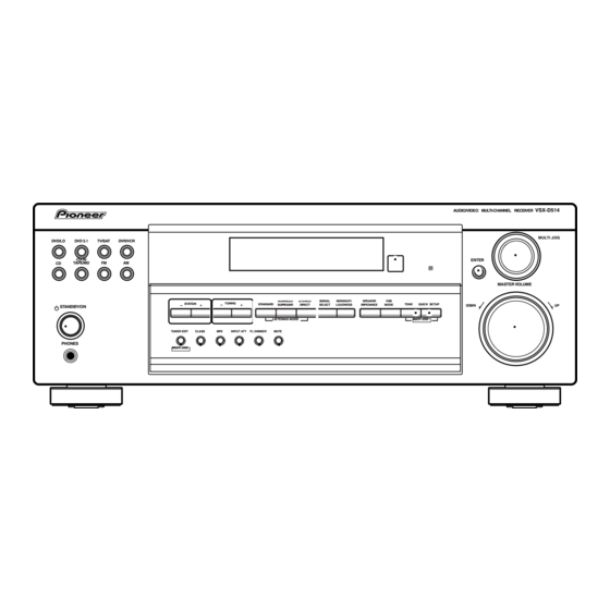
DVD/LD
DVD 5.1
TV/SAT
CD-R/
CD
TAPE/MD
FM
STANDBY / ON
PHONES
Power Requirement
AC120V
AC120V
AC120V
AC120V
4-1, Meguro 1-chome, Meguro-ku, Tokyo 153-8654, Japan
AUDIO/VIDEO MULTI-CHANNEL RECEIVER
DVR/VCR
ENTER
AM
MASTER VOLUME
ADVANCED
STEREO/
SIGNAL
MIDNIGHT/
SPEAKER
VSB
STATION
TUNING
STANDARD
TONE
QUICK SETUP
SURROUND
DIRECT
SELECT
LOUDNESS
IMPEDANCE
MODE
DO WN
LISTENING MODE
MULTI JOG
TUNER EDIT
CLASS
MPX
INPUT ATT
FL DIMMER
MUTE
MULTI JOG
VSX-D514-K
VSX-D514
MULTI JOG
UP
ORDER NO.
RRV2901
Remarks
ZZK FEB. 2004 printed in Japan
Advertisement
Table of Contents


Need help?
Do you have a question about the VSX-D514-S and is the answer not in the manual?
Questions and answers