Advertisement
Table of Contents
- 1 Specifications
- 2 Circuit Description
- 3 PLL Synthesizer
- 4 Required Test Equipment
- 5 Transmit Power Adjustment
- 6 TX Deviation Adjustment
- 7 Receiver Front-End Adjustment
- 8 Sub Receiver Front-End Adjustment
- 9 Software Alignment/Confirmation Mode
- 10 Main Unit
- 11 Parts List
- 12 Cntl Unit
- 13 Circuit Diagram
- 14 Parts Layout
- 15 MIC Unit
- Download this manual
See also:
Owner's Manual
Advertisement
Table of Contents

Related Manuals for Standard Horizon QUEST-X GX1500S


Summary of Contents for Standard Horizon QUEST-X GX1500S
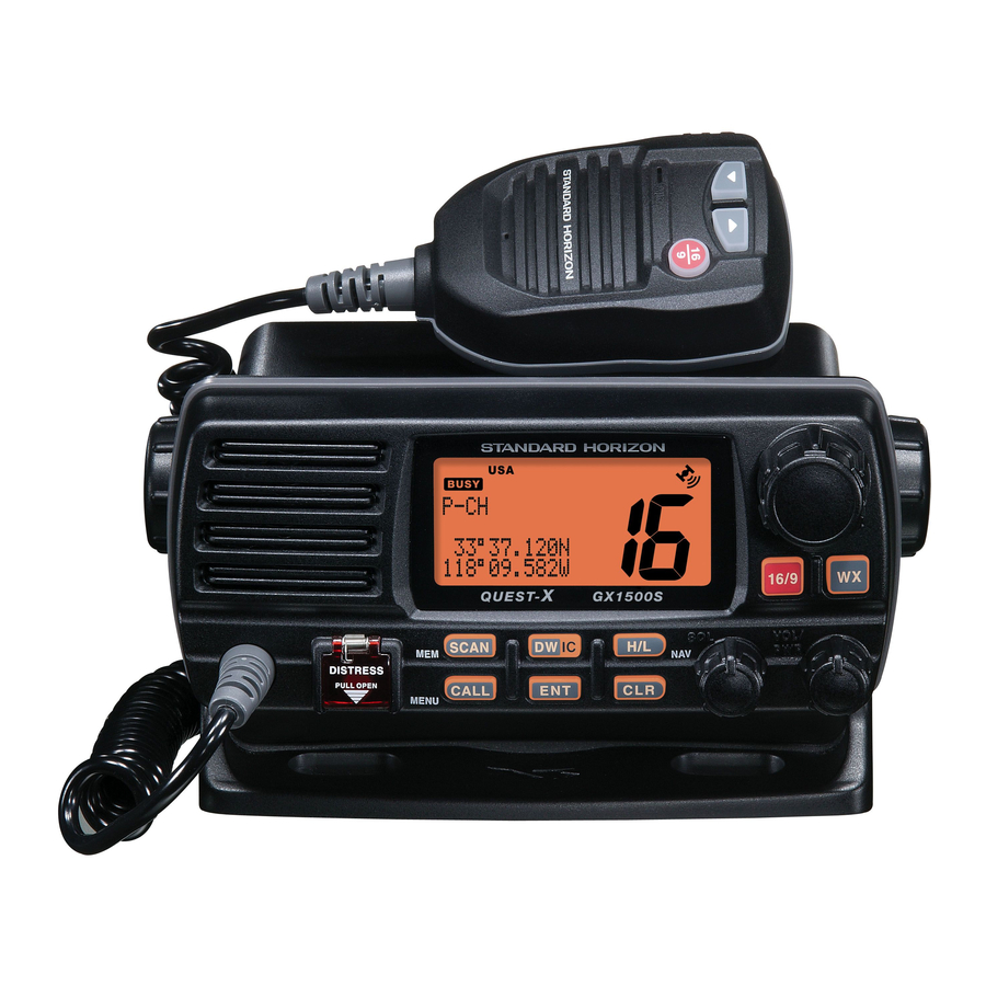
- Page 1 25 Watt VHF/FM Marine Transceiver QUEST-X GX1500S SERVICE MANUAL EM017N90A...
-
Page 2: Specifications
Specifications GENERAL Channels: All USA, International, and Canadian Input Voltage: 13.8 VDC ±20% Current Drain: Standby 0.4 A Receive 1.5 A Transmit 5.5 A (Hi); 1.5 A (Lo) Dimensions (H x W x D): 3.1” x 7” x 5.7” (80 x 180 x 145 mm) Flush-Mount Dimensions (H x W x D): 2.5”... - Page 3 Exploded View & Miscellaneous Parts RA0747100 (WHITE) RA0765100 (BLACK) HOOK RA0423200 RA0757400 (WHITE) RA0745700 (WHITE) LOCK PLATE RA0758400 (BLACK) RA0745800 (BLACK) SLEEVE RA0493800 REAR CASE LOCK PLATE (DC CABLE) RA0746800 RA0756800 RUBBER PACKING RA0434100 RUBBER PACKING (R) RA0746100 SHEET MAIN UNIT HOLDER (PTT) RA0746000 MIC UNIT...
- Page 4 Exploded View & Miscellaneous Parts...
- Page 5 Connection Diagram...
- Page 6 Block Diagram...
-
Page 7: Circuit Description
Circuit Description and Q1050 (both 2SC4154E), then the signal is through Reception and transmission are switched by 16-bit MPU IC Q2003 (M30624FGPGP) on the CNTL Unit. The re- the AF selecor switch Q1036 (CD4066BPW). The selected ceiver uses double-conversion superheterodyne circuit- signal is passed through the AF Mute switch Q1047 ry, with a 21.4 MHz 1st IF and 450 kHz 2nd IF. - Page 8 Circuit Description Buffered output from the TX & SUB VCO Q1025 (2SK520) Transmitter is amplified by Q1024 and Q1020 (both 2SC5006) and Voice audio from the microphone is delivered to the bandpass filtered by coils L1021 & L1022 and capacitors MAIN Unit.
- Page 9 Circuit Description VCO output passes through buffer amplifier Q1024 (2SC5006) to obtain stable output. Operation is controlled by 16-bit MPU IC Q2003 (M30624FGPGP). The system clock uses a 14.74560 MHz 1050 Hz Weather Alert Decoder crystal for a time base. IC Q2002 (PST597CN) resets the 1050 Hz Weather Alert signal from the FM IF subsystem MPU when the power is on, and monitors the voltage of IC Q1039 (TA31136FN) is demodulated by Q1049...
- Page 10 Circuit Description Note...
-
Page 11: Required Test Equipment
Correct alignment requires that the ambient temperature covered by the warranty policy. Also, Standard Horizon, be the same as that of the transceiver and test equipment, a division of Vertex Standard must reserve the right to and that this temperature be held constant between 68 °F... -
Page 12: Transmit Power Adjustment
Alignment Reference Frequency Adjustment Sub Receiver/Transmitter VCV Adjustment Setup the test equipment as shown below. Setup the test equipment as shown below. Sampling Coupler 50-ohm GX1500S 50-ohm DC Voltmeter GX1500S Dummy Load TP1007 Dummy Load Set the channel to CH16. With the PTT switch pressed, adjust TC1001 so that Frequency the DC voltmeter reading is 3.0 V ±... -
Page 13: Tx Deviation Adjustment
Alignment TX Deviation Adjustment Receiver Front-end Adjustment Setup the test equipment as shown below. Setup the test equipment as shown below. Sampling Coupler Tracking Spectrum GX1500S 50-ohm AF Signal GX1500S Generator TP1006 Analizer J1001 Dummy Load Generator Pin 2 Set the spectrum analyzer as shown below: CENTER: 159.000 MHz Deviation SPAN: 20.000 MHz... -
Page 14: Software Alignment/Confirmation Mode
Alignment Software Alignment/Confirmation Mode TARTING OFTWARE ONFIRMATION Confirm that the transceiver’s power is turned off. The “Software Alignment/Confirmation Mode” has been Short the TEST points (JP1001). build in the microprocessor in order to adjust and con- Press and hold the PWR key until the radio turns on firm the performance of transceiver. - Page 15 MAIN Unit Circuit Diagram RX: 1.00 V RX: 7.50 V RX: 5.75 V RX: 7.00 V RX: 7.70 V RX: 2.75 V RX: 5.30 V RX: 5.40 V RX: 0.50 V RX: 0.70 V RX: 0.25 V RX: 0.30 V RX: 7.70 V RX: 7.00 V RX: 7.40 V...
- Page 16 MAIN Unit Note...
-
Page 17: Main Unit
MAIN Unit Parts Layout (Side A) S-AV37 CD4053BPWR (Q1005) (Q1026) TA31136FN (Q1039, 1043) TB31202FNG (Q1033) LA4425A CD4066BPWR (Q1048) (Q1036) LM2902PWR (Q1051, 1052) 2SK508 (K52) LM2904PWR (Q1025) (Q1002) 2SK520 (K41) (Q1035) 2SC4154 (LE) DTA144EE (16) (Q1038, 1040, 1042) (Q1001, 1034) 2SC5006 (24) (Q1014, 1024, 1032) RT1N441U (N3) MC2850 (A7) - Page 18 MAIN Unit Parts Layout (Side B) NJM2211M NJM7808DL1A (Q1041, 1045) (Q1019) NJM78M05DL1A (Q1017) 3SK131 (V12) 3SK294 (UV) (Q1023, 1031) (Q1013, 1022) 2SB1301 (ZQ) 2SC4154 (LE) (Q1011, 1018) (Q1021, 1030, 1044, 1046, 1049, 1050) 2SC4400 (RT4) (Q1028, 1037) 2SC5006 (24) (Q1020) DTB123EK (F12) (Q1003, 1008) RT1N441U (N3)
-
Page 19: Parts List
MAIN Unit Parts List DESCRIPTION VALUE TOL. MFR'S DESIG VXSTD P/N VERS. LOT SIDE LAY ADR PCB with Components CB3333001 CB3333002 EUROPE Printed Circuit Board AM017N000 FR0139100 C 1002 CERAMIC CAP. 15pF CHU5 150J6 K02179104 C 1003 CHIP CAP. GRM1882C1H4R0CZ01D K22174205 C 1004 CERAMIC CAP. - Page 20 MAIN Unit Parts List DESCRIPTION VALUE TOL. MFR'S DESIG VXSTD P/N VERS. LOT SIDE LAY ADR C 1095 CHIP CAP. 10pF GRM1882C1H100JA01D K22174211 C 1097 CHIP CAP. 10pF GRM1882C1H100JA01D K22174211 C 1098 CHIP CAP. 10pF GRM1882C1H100JA01D K22174211 C 1099 CHIP CAP. GRM1882C1H6R0DZ01D K22174207 C 1100...
- Page 21 MAIN Unit Parts List DESCRIPTION VALUE TOL. MFR'S DESIG VXSTD P/N VERS. LOT SIDE LAY ADR C 1176 CHIP CAP. 15pF GRM1882C1H150JA01D K22174215 C 1179 CHIP CAP. GRM1884C1H1R0CZ01D K22174202 C 1180 CHIP CAP. 0.001uF GRM188B11H102KA01D K22174821 C 1182 CHIP CAP. 330pF GRM188B11H331KD01D K22174820...
- Page 22 MAIN Unit Parts List DESCRIPTION VALUE TOL. MFR'S DESIG VXSTD P/N VERS. LOT SIDE LAY ADR C 1265 CHIP TA.CAP. 10uF TEMSVA1A106M-8R K78100028 C 1277 CHIP CAP. 10pF GRM1882C1H100JA01D K22174211 C 1279 CHIP CAP. 22pF GRM1882C1H220JA01D K22174219 C 1280 CHIP CAP. 22pF GRM1882C1H220JA01D K22174219...
- Page 23 MAIN Unit Parts List DESCRIPTION VALUE TOL. MFR'S DESIG VXSTD P/N VERS. LOT SIDE LAY ADR C 1375 CHIP CAP. 0.1uF GRM188B11C104KA01D K22124805 C 1377 CHIP CAP. 0.1uF GRM188B11C104KA01D K22124805 C 1378 CHIP CAP. 0.1uF GRM188B11C104KA01D K22124805 C 1379 CHIP CAP. 0.01uF GRM188B11H103KA01D K22174823...
- Page 24 MAIN Unit Parts List DESCRIPTION VALUE TOL. MFR'S DESIG VXSTD P/N VERS. LOT SIDE LAY ADR L 1002 COIL A1 4.5T3.5D0.8UEW R L0021149A L 1003 M.RFC 4.7uH LAL03NA4R7K L1190203 L 1004 COIL A1 4.5T3.5D0.8UEW R L0021149A L 1005 COIL A1 3.5T4.0D0.8UEW R L0022245 L 1006...
- Page 25 MAIN Unit Parts List DESCRIPTION VALUE TOL. MFR'S DESIG VXSTD P/N VERS. LOT SIDE LAY ADR Q 1028 TRANSISTOR 2SC4400-3-TL G3344008C Q 1029 TRANSISTOR RT1N441U-T11-1 G3070247 Q 1030 TRANSISTOR 2SC4154-T11-1E G3341548E Q 1031 3SK131-T2B V12 G4801317B Q 1032 TRANSISTOR 2SC5006-T1 G3350068 Q 1033 TB31202FNG(TAPE)
- Page 26 MAIN Unit Parts List DESCRIPTION VALUE TOL. MFR'S DESIG VXSTD P/N VERS. LOT SIDE LAY ADR R 1052 CHIP RES. 1/16W RMC1/16 333JATP J24185333 R 1054 CHIP RES. 1/16W RMC1/16 000JATP J24185000 R 1056 CHIP RES. 2.2k 1/16W RMC1/16 222JATP J24185222 R 1057 CHIP RES.
- Page 27 MAIN Unit Parts List DESCRIPTION VALUE TOL. MFR'S DESIG VXSTD P/N VERS. LOT SIDE LAY ADR R 1136 CHIP RES. 1/16W RMC1/16 183JATP J24185183 R 1137 CHIP RES. 1/16W RMC1/16 103JATP J24185103 R 1138 CHIP RES. 5.6k 1/16W RMC1/16 562JATP J24185562 R 1139 CHIP RES.
- Page 28 MAIN Unit Parts List DESCRIPTION VALUE TOL. MFR'S DESIG VXSTD P/N VERS. LOT SIDE LAY ADR R 1216 CHIP RES. 470k 1/16W RMC1/16 474JATP J24185474 EUROPE R 1217 CHIP RES. 1/16W RMC1/16 101JATP J24185101 EUROPE R 1218 CHIP RES. 1/16W RMC1/16 223JATP J24185223 R 1219...
- Page 29 MAIN Unit Parts List DESCRIPTION VALUE TOL. MFR'S DESIG VXSTD P/N VERS. LOT SIDE LAY ADR VR1003 POT. 100k EVN-5ESX50B15 J51811104 VR1004 POT. EVN-5ESX50B54 J51811503 X 1001 XTAL DSX531S 29.95MHz DSX531S 29.950MHZ H0103316 X 1002 XTAL TOP-B 21.85MHz 21.85000MHZ H0103270 XF1001 XTAL FILTER UM-5 22.300MHZ...
- Page 30 MAIN Unit Note...
- Page 31 CNTL Unit Circuit Diagram CPU5V 13.80 V 4.90 V RESET 90 msec CONTRAST Min. 0.90 V Max. 2.64 V CONTRAST Min. 1.50 V Max. 3.24 V CONTRAST "15" 3.97 V 2.94 V 0.40 V –0.63 V –1.66 V 13.74 V 2.47 V 4.6 Vp-p 3.5 Vp-p...
- Page 32 CNTL Unit Note...
-
Page 33: Cntl Unit
CNTL Unit Parts Layout (Side A) HD66712SA (Q2008) SN74HC14APW (Q2014) 2SC4154 (LE) (Q2007 SEGMENT COMMON LCD (DS2001) - Page 34 CNTL Unit Parts Layout (Side B) M30620FCAGP AT24C128N (Q2003) (Q2004) 2SA1602A (MF) CPH6102 (AB) (Q2009, 2011) (Q2006) 2SC4154 (LE) PST597CNR (7C) (Q2005, 2010, (Q2002) 2012) HZM27WA (27A) UA78L05ACPK (D2010, 2011) (Q2001)
- Page 35 CNTL Unit Parts List DESCRIPTION VALUE TOL. MFR'S DESIG VXSTD P/N VERS. LOT SIDE LAY ADR PCB with Components CS1859001 Printed Circuit Board AM017N000 FR0139200 C 2001 CHIP CAP. 0.01uF GRM188B11H103KA01D K22174823 C 2002 CHIP TA.CAP. 10uF TEMSVC1E106M12R K78140021 C 2033 CHIP CAP.
- Page 36 CNTL Unit Parts List DESCRIPTION VALUE TOL. MFR'S DESIG VXSTD P/N VERS. LOT SIDE LAY ADR Q 2010 TRANSISTOR 2SC4154-T11-1E G3341548E Q 2011 TRANSISTOR 2SA1602A-T11-1F G3116028F Q 2012 TRANSISTOR 2SC4154-T11-1E G3341548E Q 2013 PHOTO COUPLER TLP281(GB-TP) G0090037 Q 2014 SN74HC14APW(TAPE) G1094227 R 2001 CHIP RES.
- Page 37 CNTL Unit Parts List DESCRIPTION VALUE TOL. MFR'S DESIG VXSTD P/N VERS. LOT SIDE LAY ADR R 2073 CHIP RES. 2.2k 1/16W RMC1/16 222JATP J24185222 R 2074 CHIP RES. 1/16W RMC1/16 473JATP J24185473 R 2075 CHIP RES. 2.2k 1/16W RMC1/16 222JATP J24185222 R 2076 CHIP RES.
- Page 38 CNTL Unit Note...
-
Page 39: Circuit Diagram
VR Unit Circuit Diagram Parts Layout (Side A) (Side B) Parts List DESCRIPTION VALUE TOL. MFR'S DESIG VXSTD P/N VERS. LOT SIDE LAY ADR PCB with Components CB3335001 Printed Circuit Board AM017N000 FR0139300 JP3001 WIRE ASSY AM017N VR T9207266 VR3001 POT. RK0971114 20KA/SW J60800274 VR3002 POT. - Page 40 RAM Unit Circuit Diagram Parts Layout (Side A) (Side B) Parts List DESCRIPTION VALUE TOL. MFR'S DESIG VXSTD P/N VERS. LOT SIDE LAY ADR PCB with Components CB3336001 Printed Circuit Board AM017N000 FR0139400 J 4001 CONNECTOR LTWBD-08PMMP-LC P0091397 J 4002 CONNECTOR 06FLT-SM2-TB(LF)(SN) P1091255...
-
Page 41: Mic Unit
MIC Unit Circuit Diagram... - Page 42 MIC Unit Parts Layout (Side A) (Side B) Parts List DESCRIPTION VALUE TOL. MFR'S DESIG VXSTD P/N VERS. LOT SIDE LAY ADR PCB with Components CB3449001 Printed Circuit Board AM016N000 FR0141200 C 5003 CHIP CAP. 0.001uF GRM188B11H102KA01D K22174809 MC5001 MIC. ELEMENT EM-100PT M3290029 R 5001...
- Page 44 Copyright 2006 VERTEX STANDARD CO., LTD. All rights reserved No portion of this manual may be reproduced without the permission of VERTEX STANDARD CO., LTD.
Need help?
Do you have a question about the QUEST-X GX1500S and is the answer not in the manual?
Questions and answers