Sony CDP-CE525 Service Manual
Hide thumbs
Also See for CDP-CE525:
- Operating instructions manual (32 pages) ,
- Operating instructions manual (30 pages) ,
- Limited warranty (1 page)
Table of Contents
Advertisement
Advertisement
Table of Contents

Related Manuals for Sony CDP-CE525


Summary of Contents for Sony CDP-CE525
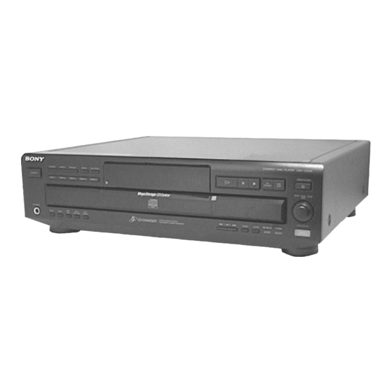
- Page 1 CDP-CE525 SERVICE MANUAL US Model Canadian Model AEP Model Australian Model Model Name Using Similar Mechanism CDP-CE515 CD Mechanism Type CDM27H Base Unit Type BU-5BD25 Optical Pick-up Type KSS-213BA/F-NP SPECIFICATIONS COMPACT DISC PLAYER MICROFILM – 1 –...
- Page 2 LES DIAGRAMMES SCHÉMATIQUES ET LA LISTE DES PIÈCES SONT CRITIQUES POUR LA SÉCURITÉ DE FONCTIONNEMENT. NE REMPLACER CES COMPOSANTS QUE PAR DES PIÈCES SONY DONT LES NUMÉROS SONT DONNÉS DANS CE MANUEL OU DANS LES SUPPLÉMENTS PUBLIÉS PAR SONY. – 2 –...
-
Page 3: Table Of Contents
TABLE OF CONTENTS 1. SERVICING NOTE ............4 2. GENERAL ................7 3. DISASSEMBLY 3-1. Case and Front Panel ............8 3-2. Back Panel and Disc Table ............ 8 3-3. Base Unit ................9 3-4. Bracket (Gear) Assembly ............9 4. -
Page 4: Servicing Note
SECTION 1 SERVICING NOTE HOW TO OPEN THE DISC TRAY WHEN POWER SWITCH TURNS OFF Insert a tapering driver into the aperture of the unit bottom, and turn in the direction of arrow (to OUT direction). * To close the disc tray, turn the driver in the reverse direction (to IN direction). - Page 5 SHIPMENT MODE Performed when returning the unit to the customer. Custom File Erases all custom files and initializes settings. Procedure: 1. Remove the discs from all trays. 2. While pressing the DISK SKIP button and PROGRAM button, press the 1/u button to turn ON the power. 3.
- Page 6 Table 2: CD-TEXT TEST DISC Recorded Contents and Display (In this unit, some special characters cannot be displayed. This is no a fault.) TRACK Recorded contents Display ! ” # $ % & ´ (21h to 27h)1kHz 0dB L&R N All the same + , –...
-
Page 7: General
SECTION 2 GENERAL Front Panel 10 11 12 13 LOCATION OF PARTS AND CONTROLS 1 1/u button 2 DISC 1-5 button 3 CONTINUE button 4 SHUFFLE button 5 PROGRAM button 6 REPEAT button 7 DISC CHECK button 8 Display window 9 ·... -
Page 8: Disassembly
SECTION 3 DISASSEMBLY Note : Follow the disassembly procedure in the numerical order given. 3-1. CASE AND FRONT PANEL 4 Case 3 Two screws 1 Two screws (BV3x8) (M3x8) !º Two screws (BVTT3x8) 2 Two screws (M3x8) 9 Flat type wire (9 core) (MAIN board, to CN403) 8 Flat type wire (17 core) (MAIN board, to CN402) -
Page 9: Base Unit
3-3. BASE UNIT 2 Screw (M3x12) 4 Two screws 3 Two screws (PTPWH2.6x6) (PTPWH2.6x6) 8 Base unit (BU-5BD25) 6 Compression spring (BU) 1 Flat type wire (16 core) (BD board, to CN101) 5 Holder (BU) 7 Compression spring (BU) 3-4. BRACKET (GEAR) ASSEMBLY 1 Stopper washer (5) 2 Gear (REV) 3 Stopper washer (5) -
Page 10: Test Mode
SECTION 4 TEST MODE ADJ MODE Buttons and Corresponding Button Numbers Button Button Number or Display NOTE : This mode cannot be performed without a general remote CONTINUE commander. 1. Chuck the CD first, and then turn OFF the power. SHUFFLE 2. - Page 11 All lit 9 10 11 12 13 14 15 16 17 18 19 20 Partial lighting 1 Light alternately Partial lighting 2 Light alternately ˜ Light alternately – 11 –...
- Page 12 AGING MODE This unit is equipped with an aging mode to check operations of the mechanism deck. • When faults occur: Aging stops, and the state when aging stopped is displayed on the fluorescent display tube. • When no fault has occurred: Aging is continued repeatedly.
-
Page 13: Electrical Block Checking
SECTION 5 ELECTRICAL BLOCK CHECKING Note: Note: 1. CD Block is basically designed to operate without adjustment. A clear RF signal waveform means that the shape “◊” can be clearly Therefore, check each item in order given. distinguished at the center of the waveform. 2. - Page 14 7. Check the level B of the oscilliscope's waveform and the A (DC voltage) of the center of the Traverse waveform. Confirm the following : A/B x 100 = less than ± 22% Traverse waveform Center of the waveform A (DC voltage) + 0.7 level : 1.3 mVp-p...
-
Page 15: Diagrams
SECTION 6 DIAGRAMS 6-1. CIRCUIT BOARDS LOCATION WAVEFORMS THIS NOTE IS COMMON FOR PRINTED WIRING BOARDS AND SCHEMATIC DIAGRAMS. (In addition to this, the necessary note is printed in each block.) 3.9Vp-p 3.7Vp-p For schematic diagrams. BD board 33.8MHz 10MHz Note: IC302 #¡... -
Page 16: Schematic Diagram - Bd Section
CDP-CE525 6-2. SCHEMATIC DIAGRAM – BD SECTION – • See page 16 for Waveforms. • See page 33 for IC Pin Functions. • See page 37 for IC Block Diagrams. (Page 23) – 17 – – 18 –... -
Page 17: Printed Wiring Board - Bd Section
CDP-CE525 6-3. PRINTED WIRING BOARD – BD SECTION – • See page 15 for Circuit Boards Location. (Page 22) • Semiconductor • Semiconductor Location Location Ref. No. Location Ref. No. Location IC102 IC101 IC103 Q101 – 19 – – 20 –... -
Page 18: Printed Wiring Board - Main Section
CDP-CE525 6-4. PRINTED WIRING BOARD – MAIN SECTION – • See page 15 for Circuit Boards Location. • Semiconductor Location Ref. No. Location D302 D321 D381 (Page 32) D601 D602 D603 D604 D605 D606 D608 D609 IC301 IC302 IC303 IC304... -
Page 19: Schematic Diagram - Main (1/2) Section
CDP-CE525 6-5. SCHEMATIC DIAGRAM – MAIN (1/2) SECTION – • See page 16 for Waveforms. • See page 35 for IC Pin Functions. • See page 39 for IC Block Diagrams. (Page 29) (Page 30) (Page 27) (Page 27) (Page 25) -
Page 20: Schematic Diagram - Main (2/2) Section
CDP-XE525 6-6. SCHEMATIC DIAGRAM – MAIN (2/2) SECTION – • See page 16 for Waveforms. • See page 21 for Printed Wiring Board. • See page 39 for IC Block Diagrams. (Page (Page (Page (Page (Page – 26 – – 25 –... -
Page 21: Printed Wiring Board - Motor Section
CDP-CE525 6-7. SCHEMATIC DIAGRAM – MOTOR SECTION – 6-8. PRINTED WIRING BOARD – MOTOR SECTION – • See page 15 for Circuit Boards Location. TABLE MOTOR BOARD M801 TABLE MOTOR (11) 1 - 6 4 7 - 3 6 4 -... -
Page 22: Schematic Diagram - Panel Section
CDP-CE525 6-9. SCHEMATIC DIAGRAM – PANEL SECTION – (Page 24) (Page 23) – 30 – – 29 –... -
Page 23: Printed Wiring Board - Panel Section
CDP-CE525 6-10. PRINTED WIRING BOARD – PANEL SECTION – • Semiconductor • See page 15 for Circuit Boards Location. Location Ref. No. Location D802 D803 D804 A-10 D805 A-11 D810 A-12 IC810 IC811 Q801 Q802 (Page 21) (Page 21) – 31 –... -
Page 24: Ic Pin Functions
6-11. IC PIN FUNCTIONS Pin No. Pin Name Function • IC101 DIGITAL SIGNAL PROCESSOR (CXA2585Q) Tracking error signal input Center servo analog input Pin No. Pin Name Function DVDD – Digital power supply RFDC RF signal input XRST System reset “L” : reset ADIO Test pin (Not used) MUTE... - Page 25 • IC302 MASTER CONTROL (CXP84648-019Q) Pin Name Function Pin No. Address data output to S-RAM Address data output to S-RAM Address data output to S-RAM Address data output to S-RAM Not used Data input/output with S-RAM Data input/output with S-RAM Data input/output with S-RAM Data input/output with S-RAM Data input/output with S-RAM...
- Page 26 Pin Name Function Pin No. KEY 3 key input CD1/2/3 Remote control mode select input KEY 2 key input KEY 1 key input n Test mode input TSENS Table sensor of disc table input * FLT FL driver latch output Serial clock output LDON Optical pick-up laser diode control output...
-
Page 27: Ic Block Diagrams
6-12. IC BLOCK DIAGRAMS • BD section IC101 CXA2585Q 71 70 67 66 65 64 63 62 61 Digital VPCO Clock DVDD0 V16M Generator XRST VCTL MUTE Interface BIAS Error AVDD1 Corrector DATA XLAT CLOCK FILI Interface Digital Sub Code FILO demodurator Processor... - Page 28 IC102 BA6392FP BUFF CH1 OUT F 28 GND BUFF BUFF CH1 OUT R 27 CH4 OUT F LEVEL SHIFT CAPA IN 1 26 CH4 OUT R BUFF CH1 R IN 25 VB IN INTERFACE CH1 F IN 24 VS IN BUFF VREF IN 23 VB IN...
-
Page 29: Main Section
• Main section IC304 BA6780 IC301 CXD8567AM INIT D Vdd 2 VIN1 VIN2 SYSM L1 (+) A Vdd L FIN1 FIN2 SHIFT L2 (+) RIN1 RIN2 LATCH A Vss L 256FSO X Vss IOUT TEST1 512IN D Vss X OUT VREF MCKSEL X Vdd... -
Page 30: Exploded Views
SECTION 7 EXPLODED VIEWS NOTE: The components identified by • Abbreviation • Items marked “*” are not stocked since they are mark ! or dotted line with mark CND : Canadian model seldom required for routine service. Some delay ! are critical for safety. AUS : Australian modeel should be anticipated when ordering these items. -
Page 31: Front Panel Section
Ref. No. Part No. Description Remark Ref. No. Part No. Description Remark 3-008-600-01 EMBLEM (5-AR), SONY * 65 1-665-357-11 POWER SW BOARD 4-997-418-01 PANEL, FRONT 4-987-779-11 WINDOW (FL) 1-782-220-11 WIRE (FLAT TYPE)(9 CORE) 4-987-994-01 KNOB (AMS) 4-951-620-01 SCREW (2.6X8), +BVTP... -
Page 32: Back Panel And Disc Table Section
7-3. BACK PANEL AND DISC TABLE SECTION M801 (US,CND) (AUS) (AEP) not supplied supplied not supplied not supplied Les composants identifiés par une The components identified by marque ! sont critiques pour la mark ! or dotted line with mark ! are critical for safety. -
Page 33: Chassis Section
7-4. CHASSIS SECTION BU-5BD25 M802 not supplied T601 Les composants identifiés par une The components identified by marque ! sont critiques pour la mark ! or dotted line with mark ! are critical for safety. sécurité. Replace only with part number Ne les remplacer que par une specified. -
Page 34: Base Unit Section (Bu-5Bd25)
7-5. BASE UNIT SECTION (BU-5BD25) M101 M102 Les composants identifiés par une The components identified by mark ! or dotted line with mark marque ! sont critiques pour la ! are critical for safety. sécurité. Replace only with part number Ne les remplacer que par une specified. -
Page 35: Electrical Parts List
SECTION 8 ELECTRICAL PARTS LIST Note: • Due to standardization, replacements in the parts list • SEMICONDUCTORS The components identified by In each case, u: µ , for example: may be different from the parts specified in the mark ! or dotted line with mark uA...: µ... - Page 36 DISPLAY Ref. No. Part No. Description Remark Ref. No. Part No. Description Remark R158 1-216-111-00 METAL CHIP 390K 1/10W R806 1-249-441-11 CARBON 100K 1/4W R159 1-216-101-00 METAL CHIP 150K 1/10W R807 1-249-441-11 CARBON 100K 1/4W R808 1-249-441-11 CARBON 100K 1/4W R161 1-216-308-00 METAL CHIP 1/10W...
- Page 37 LOADING MAIN Ref. No. Part No. Description Remark Ref. No. Part No. Description Remark < RESISTOR > C402 1-163-243-11 CERAMIC CHIP 47PF C403 1-163-243-11 CERAMIC CHIP 47PF R771 1-249-401-11 CARBON 1/4W F C404 1-106-359-00 MYLAR 4700PF 200V R772 1-249-401-11 CARBON 1/4W F C405 1-130-472-00 MYLAR...
- Page 38 MAIN Ref. No. Part No. Description Remark Ref. No. Part No. Description Remark D603 8-719-210-33 DIODE EC10DS2 Q405 8-729-422-29 TRANSISTOR 2SD601A-S D604 8-719-210-33 DIODE EC10DS2 Q406 8-729-027-23 TRANSISTOR DTA114EKA-T146 D605 8-719-210-33 DIODE EC10DS2 Q502 8-729-422-29 TRANSISTOR 2SD601A-S D606 8-719-977-22 DIODE DTZ9.1 D608 8-719-016-74 DIODE 1SS352 Q503...
- Page 39 MAIN POWER SW Ref. No. Part No. Description Remark Ref. No. Part No. Description Remark R343 1-216-073-00 METAL CHIP 1/10W R550 1-216-113-00 METAL CHIP 470K 1/10W R360 1-216-295-91 SHORT R362 1-216-073-00 METAL CHIP 1/10W R551 1-216-073-00 METAL CHIP 1/10W R552 1-216-072-00 METAL CHIP 9.1K 1/10W...
- Page 40 CDP-CE525 SENSOR TABLE MOTOR Ref. No. Part No. Description Remark Ref. No. Part No. Description Remark 1-647-362-11 SENSOR BOARD ACCESSORIES & PACKING MATERIALS ************ ******************************* < CONNECTOR > 1-475-606-11 REMOTE COMMANDER (RM-DC525) 1-558-271-11 CORD, CONNECTION (AUDIO, 108cm) CN801 1-573-383-11 PIN, CONNECTOR (PC BOARD) 2P...
Need help?
Do you have a question about the CDP-CE525 and is the answer not in the manual?
Questions and answers