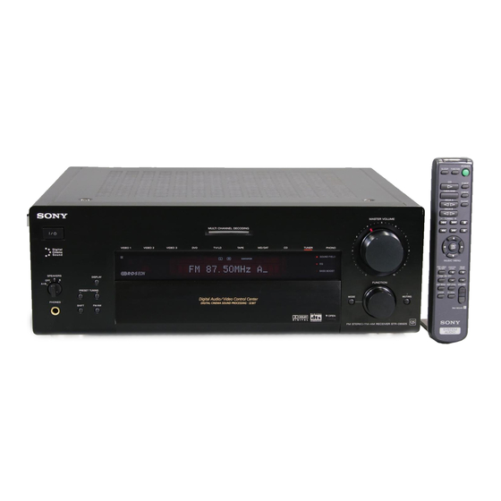
Sony STR-DB925 Service Manual
Hide thumbs
Also See for STR-DB925:
- Operating instructions manual (216 pages) ,
- Service manual (16 pages) ,
- Service manual (16 pages)

Subscribe to Our Youtube Channel
Related Manuals for Sony STR-DB925


Summary of Contents for Sony STR-DB925
- Page 1 STR-DB925 SERVICE MANUAL AEP Model UK Model Australian Model Photo: BLACK SPECIFICATIONS — Continued on next page — FM STEREO/FM-AM RECEIVER MICROFILM – 1 –...
- Page 2 WITH MARK ! ON THE SCHEMATIC DIAGRAMS AND IN THE PARTS LIST ARE CRITICAL TO SAFE OPERATION. REPLACE THESE COMPONENTS WITH SONY PARTS WHOSE PART NUMBERS APPEAR AS SHOWN IN THIS MANUAL OR IN SUPPLEMENTS PUBLISHED BY SONY. – 2 –...
-
Page 3: Table Of Contents
TABLE OF CONTENTS 1. SERVICING NOTE 3-12. Printed Wiring Board – Display Section – ....... 35 ............3 3-13. Schematic Diagram – Panel Section – ......37 3-14. Printed Wiring Board – Panel Section – ......39 2. GENERAL ................5 3-15. - Page 4 DSP SELF DIAGNOSIS FUNCTION This unit is equipped with a DSP self-diagnosis function. After completing self-diagnosis, the “DSP TEST MODE” can be set, where signals input from the external equipment will be assigned to the designated channels as shown in the table below. Table-1 Assignment of Signals in DSP TEST MODE Input Signal Output To...
-
Page 5: General
SECTION 2 GENERAL Front Panel Descriptions 2 3 4 10 11 LOCATION OF PARTS AND CONTROLS 1 1/u (power) switch 25 INPUT MODE button 2 VIDEO 1 indicator 26 5.1 INPUT button 3 VIDEO 2 indicator 27 EQ ON/OFF button 4 VIDEO 3 indicator 28 SET UP button 5 DVD indicator... -
Page 6: Diagrams
SECTION 3 DIAGRAMS 3-1. CIRCUIT BOARDS LOCATION SP-S board VIDEO board S-VIDEO board TUNER board H.P board D. IN/OUT board F-VIDEO board 5.1 IN board AUDIO board BALANCE board VOLUME board AC board REG board AMP board REAR AMP board LED board DISPLAY board JOINT board... -
Page 7: Block Diagrams
STR-DB925 3-2. BLOCK DIAGRAMS – DSP SECTION – SDTI1 SDTI2 SDTI3 119 SIC AUDATA2 BUFFER AUDATA1 118 SIB SCLK SCLK Q1207 AUDATA0 117 SIA XLAT XLAT SWDT SWDT 113 BCKO DIGITAL SIGNAL LRCK 115 LRCKO RESET RESET PROCESSOR 99 CLK1... -
Page 8: Input Section
STR-DB925 – INPUT SECTION – F MUTE DOLBY SECTION MASTER TUNER UNIT IS SUPPLIED AS THE ASSEMBLED BLOCK (Page 14) BALANCE VOLUME AUDIO SELECT SELECTOR LINE AMP TM301 IC301 IC303 IC405 IC304 RY301 RV402 RV401 SECTION TUNER UNIT -AMP- MUTE... -
Page 9: Power Section
STR-DB925 POWER AMP(L) IC501 – POWER SECTION – J701 R CH PHONES RY602 BOOSTER RELAY Q506 SWITCH DRIVE LIMITER IC414 Q601 Q504 • R CH is omitted • Signal path LIMITER CONTROL Q511 Q505 : FM PROTECTOR Q509,510 TM501 BOOSTER... -
Page 10: Dolby Section
STR-DB925 – DOLBY SECTION – L-CH A/D,D/A CONVERTER IC1103 WOOFER CENTER INPUT SECTION (Page 9, CCLK CCLK CDTI CDT1 CDTO CDTO CLOCK GENERATOR IC1107 IC1403 SDTI1 SDTI2 X1301 2CLK SCLK SDTI3 49.152MHz DOLBY DIGITAL AUDIO DECODER IC1301 IC1106 INVERTER AUDIO... - Page 11 WAVEFORMS – DIGITAL SECTION – THIS NOTE IS COMMON FOR PRINTED WIRING – DISPLAY SECTION – BOARDS AND SCHEMATIC DIAGRAMS. (In addition to this, the necessary note is printed 4Vp-p in each block.) 3.2Vp-p For schematic diagrams. 4MHz Note: IC1201 (™ XO •...
-
Page 12: Schematic Diagram - Input Section
STR-DB925 3-3. SCHEMATIC DIAGRAM – INPUT SECTION – • See page 58 for IC Block Diagrams. (Page 53) (Page 41) (Page 45) (Page 45) (Page 45) (Page 38) (Page 38) (Page 21) (Page 29) (Page 30) (Page 22) (Page 42) (Page 46) –... -
Page 13: Printed Wiring Board - Input Section
STR-DB925 3-4. PRINTED WIRING BOARD – INPUT SECTION – • See page 6 for Circuit Boards Location. (Page 48) (Page 24) (Page 31) (Page 47) (Page 23) (Page 47) • Semiconductor Location (Page 44) (Page 43) (Page 32) (Page 56) -
Page 14: Schematic Diagram - Power Amp Section
STR-DB925 3-5. SCHEMATIC DIAGRAM – POWER AMP SECTION – (Page 29) (Page 18) (Page 26) (Page 26) (Page 29) (Page 18) (Page 29) (Page 30) (Page 53) – 22 – – 21 –... -
Page 15: Printed Wiring Board - Power Amp Section
STR-DB925 3-6. PRINTED WIRING BOARD – POWER AMP SECTION – • See page 6 for Circuit Boards Location. (Page 32) (Page 20) (Page 28) (Page 28) (Page 56) (Page 31) (Page 31) (Page 32) • Semiconductor Location Ref. No. Location Ref. -
Page 16: Schematic Diagram - Trans Section
STR-DB925 3-7. SCHEMATIC DIAGRAM – TRANS SECTION – • See page 58 for IC Block Diagrams. (Page 22) (Page 22) (Page 53) – 25 – – 26 –... -
Page 17: Printed Wiring Board - Trans Section
STR-DB925 3-8. PRINTED WIRING BOARD – TRANS SECTION – • See page 6 for Circuit Boards Location. (Page 56) (Page 24) (Page 24) – 27 – – 28 –... -
Page 18: Schematic Diagram - Rear Amp Section
STR-DB925 3-9. SCHEMATIC DIAGRAM – REAR AMP SECTION – (Page 18) (Page 21) (Page 18) (Page 21) (Page 51) (Page 22) (Page 22) – 30 – – 29 –... -
Page 19: Printed Wiring Board - Rear Amp Section
STR-DB925 3-10. PRINTED WIRING BOARD – REAR AMP SECTION – • See page 6 for Circuit Boards Location. (Page 19) • Semiconductor Location Ref. No. Location D701 D702 D703 D704 D751 D752 D753 D754 Q704 Q705 Q706 Q707 Q708 Q754... -
Page 20: Schematic Diagram - Display Section
STR-DB925 3-11. SCHEMATIC DIAGRAM – DISPLAY SECTION – • See page 16 for Waveforms. • See page 57 for IC Block Diagrams. • See page 60 for IC Pin Functions. (Page 45) (Page 37) (Page 37) (Page 38) (Page 38) -
Page 21: Printed Wiring Board - Display Section
STR-DB925 3-12. PRINTED WIRING BOARD – DISPLAY SECTION – • See page 6 for Circuit Boards Location. (Page 39) (Page 39) (Page 39) (Page 47) (Page 39) (Page 56) (Page 56) (Page 43) • Semiconductor Location Ref. No. Location Ref. No. -
Page 22: Schematic Diagram - Panel Section
STR-DB925 3-13. SCHEMATIC DIAGRAM – PANEL SECTION – (Page 34) (Page 33) (Page 34) (Page 17) (Page 34) (Page 17) – 38 – – 37 –... -
Page 23: Printed Wiring Board - Panel Section
STR-DB925 3-14. PRINTED WIRING BOARD – PANEL SECTION – • See page 6 for Circuit Boards Location. (Page 36) (Page 35) (Page 35) (Page 20) (Page 20) (Page 35) – 39 – – 40 –... -
Page 24: Schematic Diagram - Back Panel Section
STR-DB925 3-15. SCHEMATIC DIAGRAM – BACK PANEL SECTION – • See page 16 for Waveforms. • See page 58 for IC Block Diagrams. (Page 42) (Page 33) (Page 41) (Page 46) (Page 17) (Page 17) (Page 51) – 42 –... -
Page 25: Printed Wiring Board - Back Panel Section
STR-DB925 3-16. PRINTED WIRING BOARD – BACK PANEL SECTION – • See page 6 for Circuit Boards Location. (Page 43) (Page 48) (Page 36) (Page 44) (Page 19) (Page 19) (Page 56) – 43 – – 44 –... -
Page 26: Schematic Diagram - Volume Section
STR-DB925 3-17. SCHEMATIC DIAGRAM – VOLUME SECTION – (Page 41) (Page 18) (Page 18) (Page 18) (Page 18) (Page 34) – 46 – – 45 –... -
Page 27: Printed Wiring Board - Volume Section
STR-DB925 3-18. PRINTED WIRING BOARD – VOLUME SECTION – • See page 6 for Circuit Boards Location. (Page 20) (Page 19) (Page 36) (Page 43) (Page 20) (Page 20) – 47 – – 48 –... -
Page 28: Schematic Diagram - D In/Out Section
STR-DB925 3-19. SCHEMATIC DIAGRAM – D IN/OUT SECTION – 3-20. PRINTED WIRING BOARD – D IN/OUT SECTION – • See page 58 for IC Block Diagrams. • See page 6 for Circuit Boards Location. (Page 56) (Page 54) – 50 –... -
Page 29: Schematic Diagram - Digital (1/2) Section
STR-DB925 3-21. SCHEMATIC DIAGRAM – DIGITAL (1/2) SECTION – • See page 16 for Waveforms. • See page 64, 67 for IC Pin Functions. • See page 55 for Printed Wiring Board. (Page 42) (Page 30) (Page 34) (Page 34) –... -
Page 30: Schematic Diagram - Digital (2/2) Section
STR-DB925 3-22. SCHEMATIC DIAGRAM – DIGITAL (2/2) SECTION – • See page 16 for Waveforms. • See page 59 for IC Block Diagrams (Page 22) (Page 25) (Page 17) (Page 49) – 54 – – 53 –... -
Page 31: Printed Wiring Board - Digital Section
STR-DB925 3-23. PRINTED WIRING BOARD – DIGITAL SECTION – • See page 6 for Circuit Boards Location. (Page 27) (Page 50) (Page 35) (Page 32) (Page 24) (Page 44) (Page 20) (Page 36) • Semiconductor Location Ref. No. Location Ref. No. -
Page 32: Ic Block Diagrams
STR-DB925 IC303 LC7823 3-24. IC BLOCK DIAGRAMS IC901 NJM2103D IC105 MSC1164GS-KR1 IC103 BA6208 MOTOR RESET L COM1 R COM1 SWITCH DRIVE DOUT – + MOTOR SWITCH DRIVE VREF L COM2 R COM2 + – OUTC VSB/SESIN L COM3 R COM3... - Page 33 IC1103 AK4526 IC1108 MC74HC00AF SDOS Clock Gen 33 VREFL MCLK OCKS RIN+ RIN- MCLK BICK BICK LIN+ LRCK LRCK 29 LIN- SDTI1 SDTI1 ROUT1 SDTI2 SDTI2 LOUT1 SDTI3 SDTI3 ROUT2 SDTO LOUT2 DAUX ROUT3 SDOUT LOUT3 Audio OCKS IC1301 CS4926 26 25 24 23 22 CMPREQ,LRCKN2 CLK IN...
-
Page 34: Ic Pin Functions
3-25. IC PIN FUNCTIONS • IC102 MB90553PF-G-121-BND (DISPLAY BOARD) Pin No. Pin Name Function VIDEO 1 VISUAL display data output to LED LED V1 VIDEO 2 AUDIO display data output to LED LED V2 VIDEO 3 VISUAL display data output to LED LED V3 DVD/LD AUDIO display data output to LED LED-DVD/LD... - Page 35 Pin No. Pin Name Function Key input 4 AD KEY IN 4 – Ground (Connected to Ground) Key input 5 AD KEY IN 5 Key input 6 AD KEY IN 6 Version input AD VERSION Model input AD MODEL Stop input STOP –...
- Page 36 Pin No. Pin Name Function – Ground (Connected to Ground) – External ceramic filter 4 MHz is connected to this terminal – External ceramic filter 4 MHz is connected to this terminal – Power supply +5 V – Not used. (Connected to Ground) —...
- Page 37 IC1101 CXD8495AQ (DIGITAL BOARD) Pin No. Pin Name Function EIAJ data and parity flag output terminal (Not used) DOUT/V EMPHA Emphasis monitor output terminal (“H” = ON) Input terminal for RC generator/oscillator Output terminal for RC generator/oscillator Microprocessor I/F select input terminal (CCB: H, SUB: L) (Connecting to Ground) CCB/SUB D.
- Page 38 IC1201 MB90574PFV-G-146-BND (DIGITAL BOARD) Pin No. Pin Name Function – Not used (Connected to Ground) — RESET RF demodulator/DIR reset To AK4526 chip select To AK4526 clock CCLK From AK4526 data input CDT1 To AK4526 data output CDTO To AK4526 reset –...
- Page 39 Pin No. Pin Name Function – Not used (Connected to Ground) — – Analog power supply +5 V AVCC – Power supply +5 V AVR+ – Ground (Connected to Ground) AVR– – Ground (Connected to Ground) AVSS – Not used (Connected to Ground) —...
- Page 40 Pin No. Pin Name Function VIDEO-A To NJM2296 video select A VIDEO-B To NJM2296 video select B VIDEO-E To NJM2296 video select E ACMUTE IC muting FUNMUTE Function muting HSTX – Hardware standby (Connected to power supply +5 V) MD 2 –...
- Page 41 IC1401 CXD2712R (DIGITAL BOARD) Pin No. Pin Name Function VSS3 – Ground 2 to 5 SOA to SOD Serial data output 6, 7 ECJ0, ECJ1 Conditional jump input terminal (7pin Connected to Ground) — No connection XHDWR HCIF data write XHDRD HCIF data read –...
- Page 42 Pin No. Pin Name Function – VSS0 Ground 92 to 94 EA13 to EA15 External RAM address output EA16 Not used Test data input “L” = normal “H” = test (Connecting to Ground) TSTA PLDIVF PLL input frequency select “L” = 256Fs “H” = 128Fs (Connecting to Ground) PLDIVB PLL output frequency select “L”...
-
Page 43: Exploded Views
SECTION 4 EXPLODED VIEWS NOTE: The components identified by • Items marked “*” are not stocked since they are • The mechanical parts with no reference number in mark ! or dotted line with mark seldom required for routine service. Some delay the exploded views are not supplied. -
Page 44: Front Panel Section
1-769-961-11 WIRE (FLAT TYPE)(11 CORE) 4-900-500-11 KNOB (BAL)(SILVER) X-3375-588-1 ESCUTCHEON (WIN) ASSY 4-900-568-01 PANEL, FRONT (BLACK) 3-703-466-00 SPRING (6600) 4-900-568-31 PANEL, FRONT (SILVER) 4-942-568-41 EMBLEM (NO.5), SONY 4-900-566-01 WINDOW 4-900-577-01 SPRING (1)(R) 4-900-572-11 FULCRUM (L) 4-900-576-01 SPRING (1)(L) 4-900-571-11 FULCRUM (R) -
Page 45: Chassis Section
4-3. CHASSIS SECTION Q706 not supplied not supplied Q705 Q707 Q756 Q755 not supplied Q757 T901 Q505 Q506 Q507 not supplied Q557 Q556 Q605 Q555 Q606 Q607 Supplied with J701 supplied Supplied with RV401 not supplied The components identified by mark ! or dotted line with mark ! are critical for safety. -
Page 46: Electrical Parts List
SECTION 5 5.1 IN ELECTRICAL PARTS LIST Note: • SEMICONDUCTORS • Due to standardization, replacements in the parts list The components identified by In each case, u: µ , for example: may be different from the parts specified in the mark ! or dotted line with mark uA...: µ... - Page 47 Ref. No. Part No. Description Remark Ref. No. Part No. Description Remark C813 1-126-022-11 ELECT 47uF < FUSE HOLDER > CC48 1-136-153-00 FILM 0.01uF CC49 1-136-153-00 FILM 0.01uF FH801 1-533-293-11 FUSE HOLDER CC98 1-136-153-00 FILM 0.01uF FH802 1-533-293-11 FUSE HOLDER FH803 1-533-293-11 FUSE HOLDER CC99...
- Page 48 AUDIO Ref. No. Part No. Description Remark Ref. No. Part No. Description Remark R539 1-249-427-11 CARBON 6.8K 1/4W F < TERMINAL > R540 1-249-417-11 CARBON 1/4W F R541 1-249-429-11 CARBON 1/4W TM501 1-694-429-21 TERMINAL BOARD (SP)(SPEAKERS FRONT) R542 1-249-429-11 CARBON 1/4W R547 1-249-425-11 CARBON...
- Page 49 BALANCE D. IN/OUT DIGITAL Ref. No. Part No. Description Remark Ref. No. Part No. Description Remark 1-670-020-11 BALANCE BOARD A-4414-117-A DIGITAL BOARD, COMPLETE ************* *********************** < CONNECTOR > < CAPACITOR > CNP106 1-564-721-11 PIN, CONNECTOR (SMALL TYPE) 5P C1101 1-163-275-11 CERAMIC CHIP 0.001uF C1102 1-126-022-11 ELECT...
- Page 50 DIGITAL Ref. No. Part No. Description Remark Ref. No. Part No. Description Remark C1204 1-165-319-11 CERAMIC CHIP 0.1uF D1205 8-719-016-74 DIODE 1SS352 C1205 1-165-319-11 CERAMIC CHIP 0.1uF D1206 8-719-801-78 DIODE 1SS184 C1206 1-163-275-11 CERAMIC CHIP 0.001uF < GROUND TERMINAL > C1207 1-165-319-11 CERAMIC CHIP 0.1uF...
- Page 51 DIGITAL Ref. No. Part No. Description Remark Ref. No. Part No. Description Remark R1113 1-216-025-91 RES,CHIP 1/10W R1173 1-216-065-91 RES,CHIP 4.7K 1/10W R1114 1-216-025-91 RES,CHIP 1/10W R1115 1-216-097-91 RES,CHIP 100K 1/10W R1174 1-216-037-00 METAL CHIP 1/10W R1175 1-216-073-00 METAL CHIP 1/10W R1116 1-216-025-91 RES,CHIP...
-
Page 52: Digital Display
DIGITAL DISPLAY Ref. No. Part No. Description Remark Ref. No. Part No. Description Remark R1249 1-216-073-00 METAL CHIP 1/10W R1321 1-216-061-00 METAL CHIP 3.3K 1/10W R1250 1-216-065-91 RES,CHIP 4.7K 1/10W R1322 1-216-061-00 METAL CHIP 3.3K 1/10W R1251 1-216-073-00 METAL CHIP 1/10W R1323 1-216-061-00 METAL CHIP... - Page 53 DISPLAY Ref. No. Part No. Description Remark Ref. No. Part No. Description Remark C185 1-162-306-11 CERAMIC 0.01uF < TRANSISTOR > C186 1-162-306-11 CERAMIC 0.01uF Q101 8-729-119-76 TRANSISTOR 2SA1175-HFE C191 1-164-159-11 CERAMIC 0.1uF Q102 8-729-900-36 TRANSISTOR DTC124ES C192 1-107-818-11 ELECT 5.5V Q103 8-729-900-36 TRANSISTOR DTC124ES Q104...
- Page 54 DISPLAY F-VIDEO INPUT Ref. No. Part No. Description Remark Ref. No. Part No. Description Remark R134 1-249-411-11 CARBON 1/4W < RESISTOR > R135 1-249-411-11 CARBON 1/4W R161 1-249-385-11 CARBON 1/6W F R297 1-247-804-11 CARBON 1/4W R298 1-247-804-11 CARBON 1/4W R162 1-249-421-11 CARBON 2.2K 1/4W F...
- Page 55 INPUT Ref. No. Part No. Description Remark Ref. No. Part No. Description Remark C416 1-126-233-11 ELECT 22uF C754 1-102-230-00 CERAMIC 0.25PF 500V C417 1-126-233-11 ELECT 22uF C418 1-126-233-11 ELECT 22uF C755 1-126-101-11 ELECT 100uF C780 1-162-282-31 CERAMIC 100PF C419 1-162-282-31 CERAMIC 100PF C789 1-162-282-31 CERAMIC...
- Page 56 INPUT Ref. No. Part No. Description Remark Ref. No. Part No. Description Remark Q302 8-729-141-30 TRANSISTOR 2SC3623A-LK R388 1-249-417-11 CARBON 1/4W F Q303 8-729-141-30 TRANSISTOR 2SC3623A-LK R389 1-249-417-11 CARBON 1/4W F Q304 8-729-141-30 TRANSISTOR 2SC3623A-LK R390 1-249-417-11 CARBON 1/4W F Q352 8-729-141-30 TRANSISTOR 2SC3623A-LK R391...
- Page 57 INPUT JOINT REAR AMP Ref. No. Part No. Description Remark Ref. No. Part No. Description Remark R751 1-249-417-11 CARBON 1/4W F < TRANSISTOR > R752 1-249-439-11 CARBON 1/4W Q704 8-729-119-76 TRANSISTOR 2SA1175-HFE R753 1-249-439-11 CARBON 1/4W Q708 8-729-140-82 TRANSISTOR 2SA988-PAFAEA R754 1-247-843-11 CARBON 3.3K...
- Page 58 ROTARY S-VIDEO Ref. No. Part No. Description Remark Ref. No. Part No. Description Remark < CONNECTOR > < RESISTOR > CNP803 1-564-320-00 PIN, CONNECTOR (B2P-VH) 2P R101 1-249-411-11 CARBON 1/4W CNP809 1-779-977-11 PIN, CONNECTOR 6P R102 1-249-411-11 CARBON 1/4W < DIODE > <...
- Page 59 S-VIDEO SP-S Ref. No. Part No. Description Remark Ref. No. Part No. Description Remark < RESISTOR > < TRANSISTOR > R251 1-247-804-11 CARBON 1/4W Q544 8-729-119-79 TRANSISTOR 2SC2785-FEK R252 1-249-429-11 CARBON 1/4W Q609 8-729-281-53 TRANSISTOR 2SC1815-GR R253 1-247-804-11 CARBON 1/4W Q610 8-729-900-63 TRANSISTOR DTA124ES R254...
- Page 60 SP SW TUNER Ref. No. Part No. Description Remark Ref. No. Part No. Description Remark 1-670-018-11 SP SW BOARD < SWITCH > *********** S103 1-762-751-11 SWITCH, TACTILE (INPUT MODE) < CONNECTOR > S104 1-762-751-11 SWITCH, TACTILE (RDS-PTY) S107 1-762-751-11 SWITCH, TACTILE (5.1 INPUT) CNS106 1-770-404-11 HOUSING,CONNECTOR(PC BOARD)11P S108 1-762-751-11 SWITCH, TACTILE (RDS-EON)
- Page 61 VIDEO VOLUME Ref. No. Part No. Description Remark Ref. No. Part No. Description Remark 1-670-003-11 VIDEO BOARD C414 1-162-199-31 CERAMIC 10PF *********** C415 1-162-199-31 CERAMIC 10PF < CAPACITOR > C421 1-162-286-31 CERAMIC 220PF C422 1-162-286-31 CERAMIC 220PF C201 1-126-964-11 ELECT 10uF C423 1-162-286-31 CERAMIC...
- Page 62 STR-DB925 Ref. No. Part No. Description Remark 1-773-163-11 WIRE (FLAT TYPE)(21 CORE) 1-769-961-11 WIRE (FLAT TYPE)(11 CORE) 1-773-285-11 WIRE (FLAT TYPE)(29 CORE) ! CNJ909 1-526-794-11 OUTLET, AC FL101 1-517-781-11 INDICATOR TUBE, FLUORESCENT Q505 8-729-209-15 TRANSISTOR 2SD2012 Q506 8-749-010-25 IC MN2488-OPY-M...
Need help?
Do you have a question about the STR-DB925 and is the answer not in the manual?
Questions and answers