Table of Contents

Related Manuals for Aiwa XP-V311


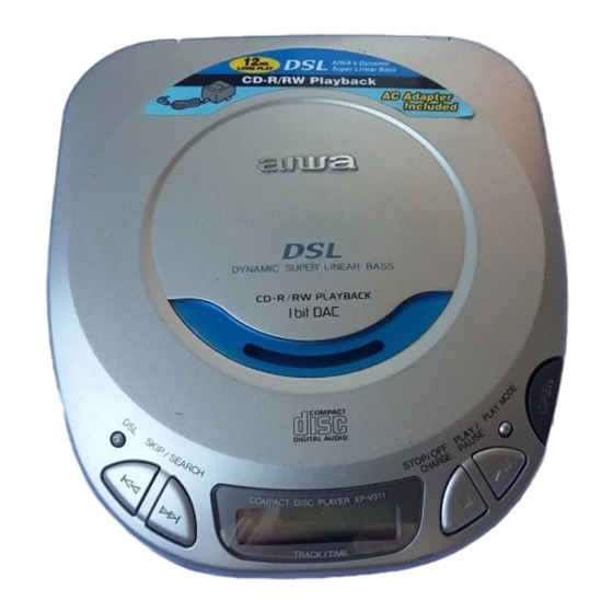
Summary of Contents for Aiwa XP-V311
- Page 1 XP-V311 ALH1(S) ALHB(S) ALH(LL) SERVICE MANUAL BASIC CD MECHANISM : DA23L COMPACT DISC PLAYER This Service Manual is the "Revision Publishing" and replaces "Simple Manual" (S/M Code No. 09-003-339-8T1). S/M Code No. 09-003-339-8R1...
-
Page 2: Protection Of Eyes From Laser Beam During Servicing
PROTECTION OF EYES FROM LASER BEAM DURING SERVICING This set employs laser. Therefore, be sure to follow carefully the CAUTION instructions below when servicing. Use of controls or adjustments or performance of procedures other than those specified herein may result in hazardous WARNING! radiation exposure. -
Page 3: Specifications
SPECIFICATIONS • Design and specifications are subject to change without notice... -
Page 4: Electrical Main Parts List
ELECTRICAL MAIN PARTS LIST REF. NO PART NO. KANRI DESCRIPTION REF. NO PART NO. KANRI DESCRIPTION C354 87-010-196-080 CHIP CAPACITOR,0.1-25 C355 87-010-312-080 C-CAP,S 15P-50 CH 87-A21-448-040 C-IC,BH6554FV C356 87-010-312-080 C-CAP,S 15P-50 CH 87-A21-083-040 C-IC,BH6508FS C357 87-010-196-080 CHIP CAPACITOR,0.1-25 87-A21-381-040 C-IC,LA9235M C358 87-010-322-080 C-CAP,S 100P-50 CH... -
Page 5: Chip Resistor Part Code
REF. NO PART NO. KANRI DESCRIPTION VR701 87-A90-462-010 VR,RTRY 30KCX2 H RK14J12A0 X351 87-A70-202-080 C-VIB,CER 16.93MHZ CSACV-MXJ04 • Regarding connectors, they are not stocked as they are not the initial order items. The connectors are available after they are supplied from connector manufacturers upon the order is received. CHIP RESISTOR PART CODE Chip Resistor Part Coding Figure... -
Page 6: Lcd Display
LCD DISPLAY... -
Page 7: Schematic Diagram
SCHEMATIC DIAGRAM... - Page 8 WIRING SF-P200...
-
Page 9: Test Mode
TEST MODE IC101 IC351 IC301 IC201 Q305 IC701 IC801 TEST MODE SHORT LAND... -
Page 10: Startup Procedure
The servo circuit of this model has been designed to be free of adjustments and controlled within the IC. Therefore, adjustments and disk judgement are performed automatically every time the TOC is read out. The adjustment status of each servo inside the IC can be monitored in this test mode. - Page 11 4. Amount of change of jitter The amount of change of jitter is displayed in the focus bias check mode. The displayed value has 256 steps from 00 to FF. Example: focus bias (FB) Adjustment value™00 Jitter value™FD RNDM RESUME Tracking offset Adjustment value * Adjustment values and jitter values are indicated in hexadecimal.
- Page 12 WAVE FORM IC301 Pin ≥ VOLT/DIV: 0.2V IC601 Pin ∞ VOLT/DIV: 0.1V TIME/DIV: 0.5µS SPDO TIME/DIV: 5mS IC301 Pin * VOLT/DIV: 0.2V TIME/DIV: 50µS IC301 Pin ¡ VOLT/DIV: 0.1V TIME/DIV: 2mS IC351 Pin VOLT/DIV: 1V XOUT TIME/DIV: 50nS f=16.93MHz IC801 Pin VOLT/DIV: 1V TIME/DIV: 0.2µS f=4.2MHz...
- Page 13 IC BLOCK DIAGRAM IC, BH6508FS IC, BH6554FV IC, TA2120FN...
- Page 14 IC DESCRIPTION IC, LC78641NE-D Pin No. Pin Name Description PDO1 Internal VCD control phase comparator output pin. Internal VCD control phase comparator output pin. OFF for rough servo, ON for phase PDO2 servo. VVSS — Internal VCD ground pin. PCKIST PDO output current adjustment resistor connection pin.
- Page 15 Pin No. Pin Name Description DOUT Digital OUT output pin. (EIAJ format) Output pin for the 7.35kHz synchronization signal divided from the crystal osillator. EFLG C1 C2 error correction monitor pin. Test input pin. Must be connected to OV. TEST Emphasis pin.
- Page 16 Pin No. Pin Name Description Microprocessor interface power supply. (2000pF or more path controller to be inserted VDD5V — at a point nearer to the pin between this pin and GND) — Digital ground pin. Must be connected to 0V. CONT6 General-purpose input/output pin 6.
- Page 17 IC, µPD789405AGC-013 IC, LA9253M Pin No. Pin Name Description Pin No. Pin Name Description VDO1 — Positive polarity power supply (except for port section). FIN1 BIAS — Feeding the LCD drive power supply voltage. FIN2 Pick-up signal input. VLC0-VLC2 — LCD drive power supply voltage.
-
Page 18: Mechanical Exploded View
MECHANICAL EXPLODED VIEW 1/1 MECHANICAL PARTS LIST 1/1 REF. NO PART NO. KANRI DESCRIPTION 1 8A-HC7-007-010 WINDOW,CD 2 8A-HC7-005-010 WINDOW,DISPLAY 3 8A-HC7-040-010 LID ASSY,CD 311<LHB,LHS> 3 8A-HC7-037-010 LID ASSY,CD 311 (LL)<LHLL> 4 85-HC6-205-110 SHAFT,LID(300) HK DA23L 5 8A-HC7-204-010 SPR-T,OPEN 6 8A-HC7-018-010 LEVER,OPEN 7 8A-HC7-015-010 CABI ASSY,CENTER<LHB,LHS>... -
Page 19: Cd Mechanism Exploded View
CD MECHANISM EXPLODED VIEW 1/1 CD MECHANISM PARTS LIST REF. NO PART NO. KANRI DESCRIPTION 1 S0-A41-A20-600 PICKUP LASER ASSY 2 SM-10A-108-001 MOTOR ASSY SPINDLE 3 S0-M10-A10-900 MOTOR SLED ASSY 4 S2-311-A12-200 CHASSIS 5 S2-511-A23-200 GEAR MIDDLE 6 S2-511-A23-100 GEAR,SCREW 7 S2-511-A23-400 GEAR,RACK 8 S2-511-A07-900... -
Page 20: Accessories/Package List
ACCESSORIES/PACKAGE LIST REF. NO PART NO. KANRI DESCRIPTION 1 87-B30-285-010 AC ADAPTOR,AC-D603HRNC 2 87-B30-326-010 HEADPHONE,HP-M048 3 8A-HC7-914-010 IB,LH(3L)C F 4 87-A90-312-010 PLUG,CONVERSION WTN-1157R1 2–11, IKENOHATA 1–CHOME, TAITO-KU, TOKYO 110, JAPAN TEL:03 (3827) 3111 737004 Printed in Singapore...