Table of Contents
Advertisement
S
ervice
M anua l
MULTI-CD CONTROL DSP CD PLAYER WITH RDS/ID-LOGIC TUNER
DEX-P1R
MULTI-CD CONTROL DSP HIGH POWER CD PLAYER WITH FM/AM TUNER
DEH-P946
MULTI-CD CONTROL DSP CD PLAYER WITH FM/AM TUNER
DEX-P1
- See the separate manual CX-680(CRT2216) for the CD mechanism description, disassembly and circuit
description.
- The CD mechanism employed in this model is one of H1 series.
CONTENTS
1. SAFETY INFORMATION ............................................2
2. EXPLODED VIEWS AND PARTS LIST .......................3
3. SCHEMATIC DIAGRAM ...........................................18
4. PCB CONNECTION DIAGRAM ................................56
5. ELECTRICAL PARTS LIST ........................................74
6. ADJUSTMENT..........................................................92
PIONEER ELECTRONIC CORPORATION
PIONEER ELECTRONICS SERVICE INC.
PIONEER ELECTRONIC [EUROPE] N.V.
PIONEER ELECTRONICS ASIACENTRE PTE.LTD. 501 Orchard Road, #10-00, Lane Wheelock Place, Singapore 238880
C PIONEER ELECTRONIC CORPORATION 1998
DEX-P1R/UC
ES
4-1, Meguro 1-Chome, Meguro-ku, Tokyo 153-8654, Japan
P.O.Box 1760, Long Beach, CA 90801-1760 U.S.A.
Haven 1087 Keetberglaan 1, 9120 Melsele, Belgium
ES
7. GENERAL INFORMATION .......................................98
7.1 PARTS .................................................................98
7.1.1 IC................................................................98
7.1.2 DISPLAY ..................................................117
7.2 DIAGNOSIS ......................................................119
7.2.1 DISASSEMBLY .......................................119
7.2.2 TEST MODE ............................................120
7.3 BLOCK DIAGRAM ............................................124
8. OPERATIONS AND SPECIFICATIONS...................126
K-FEA. JUNE 1998 Printed in Japan
ORDER NO.
CRT2206
UC
Advertisement
Table of Contents

Related Manuals for Pioneer DEX-P1R


Summary of Contents for Pioneer DEX-P1R
-
Page 1: Table Of Contents
P.O.Box 1760, Long Beach, CA 90801-1760 U.S.A. PIONEER ELECTRONIC [EUROPE] N.V. Haven 1087 Keetberglaan 1, 9120 Melsele, Belgium PIONEER ELECTRONICS ASIACENTRE PTE.LTD. 501 Orchard Road, #10-00, Lane Wheelock Place, Singapore 238880 C PIONEER ELECTRONIC CORPORATION 1998 K-FEA. JUNE 1998 Printed in Japan... -
Page 2: Safety Information
DEX-P1R,DEH-P946,DEX-P1 - CD Player Service Precautions 2. During disassembly, be sure to turn the power off 1. For pickup unit(CXX1290) handling, please refer since an internal IC might be destroyed when a con- to"Disassembly"(CX-680 Service Manual CRT2216). nector is plugged or unplugged. -
Page 3: Exploded Views And Parts List
DEX-P1R,DEH-P946,DEX-P1 2. EXPLODED VIEWS AND PARTS LIST 2.1 PACKING - DEX-P1R/UC, DEX-P1/ES... - Page 4 DEX-P1R,DEH-P946,DEX-P1 NOTE: - Parts marked by "*"are generally unavailable because they are not in our Master Spare Parts List. ∇ mark on the product are used for disassembly. - Screws adjacent to - PACKING SECTION PARTS LIST (1) PARTS LIST Mark No.
- Page 5 DEX-P1R,DEH-P946,DEX-P1 (2) CONTRAST TABLE DEX-P1R/UC and DEX-P1/ES are constructed same except for the following: Part No. Mark No. Symbol and Description DEX-P1R/UC DEX-P1/ES 9 Screw CBA-102 Not used 13 Nut NF50FMC Not used 15 Strap CNF-111 Not used 19 Polyethylene Bag...
- Page 6 DEX-P1R,DEH-P946,DEX-P1 - DEH-P946/ES...
- Page 7 DEX-P1R,DEH-P946,DEX-P1 - PACKING SECTION PARTS LIST Mark No. Description Part No. Mark No. Description Part No. 1 ••••• * 16-6 Card CRP1183 2 Screw BNC40P120FZK * 16-7 Card CRP1186 3 Screw BPZ30P100FZK 17 Air Cushioned Bag CEG1192 4 Bracket CZN6467...
- Page 8 DEX-P1R,DEH-P946,DEX-P1 2.2 EXTERIOR (1) - DEX-P1R/UC, DEX-P1/ES 154 154 32 47 122 16...
- Page 9 DEX-P1R,DEH-P946,DEX-P1 - EXTERIOR (1) SECTION PARTS LIST (1) PARTS LIST Mark No. Description Part No. Mark No. Description Part No. 1 Screw BMZ30P040FMC 46 Connector(CN681) CKS3583 2 Screw BSZ26P050FMC 47 Connector(CN222) CKS3781 3 Screw BSZ30P055FMC 48 Holder CNC8011 4 Cord Assy CDE5785 49 •••••...
- Page 10 122 Bush CNV1917 156 Cushion CNM6065 123 ••••• 124 ••••• 125 ••••• (2) CONTRAST TABLE DEX-P1R/UC and DEX-P1/ES are constructed same except for the following: Part No. Mark No. Description DEX-P1R/UC DEX-P1/ES 6 Cord Assy CDE5538 CDE5539 30 Tuner Amp Unit...
- Page 11 DEX-P1R,DEH-P946,DEX-P1 - DEH-P946/ES 124 125...
- Page 12 DEX-P1R,DEH-P946,DEX-P1 - EXTERIOR (1) SECTION PARTS LIST Mark No. Description Part No. Mark No. Description Part No. 1 Screw BSZ26P050FMC 46 Connector(CN681) CKS3583 2 Screw BSZ30P055FMC 47 Connector(CN231) CKS3592 3 Cord Assy CDE5785 48 Connector(CN222) CKS3781 4 Cord CDE5536 49 Holder...
- Page 13 DEX-P1R,DEH-P946,DEX-P1 Mark No. Description Part No. Mark No. Description Part No. 91 Lighting Conductor CNV5276 116 IC(IC941) PA2024A 92 Guide CNV5356 117 IC(IC871) NJM78M05FA 93 Gathering PCB CNX2961 118 Transistor(Q992) 2SD2396 94 Mini Jack(CN4602) CKN1015 119 ••••• 95 Plug(CN4601) CKS-786...
- Page 14 10 Keyboard Unit 20 EL(EL1901) CEL1580 See Contrast table(2) 21 Spacer CNM6021 22 PCB CNP5063 (2) CONTRAST TABLE DEX-P1R/UC and DEX-P1/ES are constructed same except for the following: Part No. Mark No. Description DEX-P1R/UC DEX-P1/ES 8 Button CAC5638 CAC5498 10 Keyboard Unit...
- Page 15 DEX-P1R,DEH-P946,DEX-P1 - DEH-P946/ES - EXTERIOR (2) SECTION PARTS LIST Mark No. Description Part No. Mark No. Description Part No. 1 ••••• 11 Plug(CN1901) CKS2496 2 Button(+,−) CAC5486 12 Holder CNC7547 3 Button(OPEN/EJECT) CAC5488 13 Spacer CNM5622 4 Button(S/A,CLOCK) CAC5490 14 Spacer...
- Page 16 DEX-P1R,DEH-P946,DEX-P1 2.4 CD MECHANISM MODULE...
- Page 17 DEX-P1R,DEH-P946,DEX-P1 - CD MECHANISM MODULE SECTION PARTS LIST Mark No. Description Part No. Mark No. Description Part No. 1 Control Unit CWX2166 51 Spring CBH2039 2 Connector(CN701) CKS1968 52 Lack CNV5471 3 Connector(CN802) CKS3477 53 Bracket Unit CXB1674 4 Connector(CN801)
-
Page 18: Schematic Diagram
DEX-P1R,DEH-P946,DEX-P1 3. SCHEMATIC DIAGRAM 3.1 OVERALL CONNECTION DIAGRAM(GUIDE PAGE) Note: When ordering service parts, be sure to refer to “EXPLODED VIEWS AND PARTS LIST” or “ELECTRICAL PARTS LIST”. - DEX-P1R/UC Large size SCH diagram M.CD:+2.2dBs Guide page M.CD:+2.2dBs 4.1V FM100%:-20dBs AM30%:-26.0dBs... - Page 19 DEX-P1R,DEH-P946,DEX-P1 E G H M.CD:+13.8dBs FM100%:+7.85dBs AM30%:+1.85dBs CN3001 CN702...
- Page 20 DEX-P1R,DEH-P946,DEX-P1...
- Page 21 DEX-P1R,DEH-P946,DEX-P1...
- Page 22 DEX-P1R,DEH-P946,DEX-P1...
- Page 23 DEX-P1R,DEH-P946,DEX-P1...
- Page 24 DEX-P1R,DEH-P946,DEX-P1 3.2 OVERALL CONNECTION DIAGRAM(GUIDE PAGE) - DEH-P946/ES,DEX-P1/ES Large size SCH diagram M.CD:+2.2dBs Guide page Detailed page M.CD:+2.2dBs 4.1V FM100%:-20.0dBs AM30%:-26.0dBs FM100%:-20.0dBs AM30%:-26.0dBs FLAP SENSE PCB...
- Page 25 DEX-P1R,DEH-P946,DEX-P1 DEH-P946/ES ONLY E G H M.CD:+37.1dBs FM100%:+31.15dBs AM30%:25.15dBs DEH-P946/ES:22K DEX-P1/ES:11K DEX-P1/ES ONLY CN3001 DEH-P946/ES ONLY CN702 DEX-P1/ES ONLY 10A(DEH-P946/ES) 4A(DEX-P1/ES) C943:47/10 (DEH-P946/ES) 47/25 (DEX-P1/ES) DEX-P1/ES ONLY DEH-P946/ES ONLY...
- Page 26 DEX-P1R,DEH-P946,DEX-P1...
- Page 27 DEX-P1R,DEH-P946,DEX-P1...
- Page 28 DEX-P1R,DEH-P946,DEX-P1...
- Page 29 DEX-P1R,DEH-P946,DEX-P1...
- Page 30 DEX-P1R,DEH-P946,DEX-P1 3.3 CD MECHANISM MODULE(GUIDE PAGE) Large size SCH diagram Guide page Detailed page...
- Page 31 DEX-P1R,DEH-P946,DEX-P1...
- Page 32 DEX-P1R,DEH-P946,DEX-P1...
- Page 33 DEX-P1R,DEH-P946,DEX-P1...
- Page 34 DEX-P1R,DEH-P946,DEX-P1...
- Page 35 DEX-P1R,DEH-P946,DEX-P1...
- Page 36 DEX-P1R,DEH-P946,DEX-P1 Note:1. The encircled numbers denote measuring pointes in the circuit diagram. 2. Reference voltage - Waveforms REFO:2.5V 1 RFO 1 CH1: RFO 1 CH1: RFO 0.5V/div. 0.5µs/div. 1V/div. 1V/div. 0.5ms/div. 0.5ms/div. 2 CH2: MIRR 2 CH2: MIRR Normal mode: play 5V/div.
- Page 37 DEX-P1R,DEH-P946,DEX-P1 8 CH1: TEY 8 CH1: TEY 0 SIN 0.2V/div. 0.5V/div. 0.5V/div. 0.1s/div. 5ms/div. 20ms/div. 9 CH2: TIN ! CH2: SD 0.2V/div. 0.5V/div. Normal mode: play Normal mode: Play (12cm) → REFO → REFO → REFO → → REFO REFO...
- Page 38 DEX-P1R,DEH-P946,DEX-P1 ( CH1: R OUT 6 CH1: FEY 8 CH1: TEY 0.2V/div. 1V/div. 0.2V/div. 0.2ms/div. 1ms/div. 1ms/div. ) CH2: L OUT 3 CH2: FIN 9 CH2: TIN 1V/div. 0.5V/div. 0.5V/div. Normal mode: Play (1kHz 0dB) Normal mode: During AGC Normal mode: During AGC →...
- Page 39 DEX-P1R,DEH-P946,DEX-P1...
- Page 40 DEX-P1R,DEH-P946,DEX-P1 3.3 FM/AM TUNER UNIT - DEX-P1R/UC...
- Page 41 DEX-P1R,DEH-P946,DEX-P1...
- Page 42 DEX-P1R,DEH-P946,DEX-P1 3.4 FM/AM TUNER UNIT - DEH-P946/ES,DEX-P1/ES...
- Page 43 DEX-P1R,DEH-P946,DEX-P1...
- Page 44 DEX-P1R,DEH-P946,DEX-P1 3.5 KEYBOARD PCB...
- Page 45 DEX-P1R,DEH-P946,DEX-P1 CAW1470(DEX-P1R/UC) CAW1471(DEH-P946/ES,DEX-P1/ES)
- Page 46 DEX-P1R,DEH-P946,DEX-P1 3.6 DSP UNIT(GUIDE PAGE) Large size SCH diagram Guide page M.CD:+4.5dBs FM100%:-1.45dBs AM30%:-14.45dBs Detailed page...
- Page 47 DEX-P1R,DEH-P946,DEX-P1 :ANALOG AUDIO INPUT :DIGITAL AUDIO :FRONT AUDIO OUTPUT (Front/Miid) :FRONT AUDIO DIGITAL :REAR AUDIO OUTPUT (Rear/Hi) :REAR AUDIO DIGITAL :SUBWOOFER AUDIO OUTPUT :SUBWOOFER AUDIO DIGITAL (Sub.w/Low) DSP UNIT M.CD:+6.5dBs FM100%:+0.55dBs M,CD:+2.1dBs AM30%:-12.45dBs FM100%:-4.45dBs AM30%:-17.45dBs...
- Page 48 DEX-P1R,DEH-P946,DEX-P1...
- Page 49 DEX-P1R,DEH-P946,DEX-P1...
- Page 50 DEX-P1R,DEH-P946,DEX-P1...
- Page 51 DEX-P1R,DEH-P946,DEX-P1...
- Page 52 DEX-P1R,DEH-P946,DEX-P1 3.7 ASL UNIT...
- Page 53 DEX-P1R,DEH-P946,DEX-P1 3.8 MICROPHONE JACK UNIT MICROPHONE JACK UNIT...
- Page 54 DEX-P1R,DEH-P946,DEX-P1 3.9 HIGH OUT UNIT (DEX-P1R/UC,DEX-P1/ES) M.CD:+13.72dBs FM100%:+7.77dBs AM30%:+1.77dBs CN4003 CN4002 CN4001 CN4004...
- Page 55 DEX-P1R,DEH-P946,DEX-P1 3.10 D/D CONVERTER UNIT (DEX-P1R/UC,DEX-P1/ES) D/D CONVERTER UNIT...
-
Page 56: Pcb Connection Diagram
DEX-P1R,DEH-P946,DEX-P1 NOTE FOR PCB DIAGRAMS 1. The parts mounted on this PCB include all necessary parts for several destination. For further information for respective destinations, be sure to 4. PCB CONNECTION DIAGRAM check with the schematic diagram. MAIN ANT. CORD ASSY 4.1 TUNER AMP UNIT... - Page 57 DEX-P1R,DEH-P946,DEX-P1 2. Viewpoint of PCB diagrams Capacitor Connector SIDE A SIDE A SIDE B P.C.Board Chip Part CN701 INVERTER ASSY CN1901...
- Page 58 DEX-P1R,DEH-P946,DEX-P1 TUNER AMP UNIT...
- Page 59 DEX-P1R,DEH-P946,DEX-P1 SIDE B...
- Page 60 DEX-P1R,DEH-P946,DEX-P1 4.2 FM/AM TUNER UNIT SIDE A...
- Page 61 DEX-P1R,DEH-P946,DEX-P1 SIDE B...
- Page 62 DEX-P1R,DEH-P946,DEX-P1 4.3 CD MECHANISM MODULE SIDE A CONTROL UNIT...
- Page 63 DEX-P1R,DEH-P946,DEX-P1 SIDE B CONTROL UNIT REFO PICKUP UNIT CN671 SPINDLE MOTOR CN221...
- Page 64 DEX-P1R,DEH-P946,DEX-P1...
- Page 65 DEX-P1R,DEH-P946,DEX-P1...
-
Page 66: Keyboard Unit
DEX-P1R,DEH-P946,DEX-P1 4.4 KEYBOARD UNIT KEYBOARD UNIT KEYBOARD UNIT CN801... - Page 67 DEX-P1R,DEH-P946,DEX-P1 SIDE A SIDE B...
- Page 68 DEX-P1R,DEH-P946,DEX-P1 4.5 DSP UNIT SIDE A DSP UNIT...
- Page 69 DEX-P1R,DEH-P946,DEX-P1 SIDE B DSP UNIT CN222...
- Page 70 DEX-P1R,DEH-P946,DEX-P1 4.6 ASL UNIT SIDE A ASL UNIT CN141 SIDE B ASL UNIT...
- Page 71 DEX-P1R,DEH-P946,DEX-P1 4.7 FLAP SENSE PCB, MICROPHONE JACK UNIT FLAP SENSE PCB CN852 SIDE B SIDE A MICROPHONE JACK UNIT MICROPHONE JACK UNIT CN131...
- Page 72 DEX-P1R,DEH-P946,DEX-P1 4.8 D/D CONVERTER UNIT, D/D CONVERTER PCB (DEX-P1R/UC, DEX-P1/ES) SIDE A SIDE B D/D CONVERTER UNIT D/D CONVERTER UNIT D/D CONVERTER PCB D/D CONVERTER PCB SIDE A SIDE B CN4004 CN4002 CN4003 CN251 CN4001...
- Page 73 DEX-P1R,DEH-P946,DEX-P1 4.9 HIGH OUT PCB (DEX-P1R/UC, DEX-P1/ES) SIDE A HIGH OUT PCB RCA OUT CN231 CN252 SIDE B HIGH OUT PCB...
-
Page 74: Electrical Parts List
=====Circuit Symbol and No.===Part Name Part No. =====Circuit Symbol and No.===Part Name Part No. ------ ------------------------------------------ ------------------------- ------ ------------------------------------------ ------------------------- Unit Number : CWE1472(DEX-P1R/UC) RESISTORS Unit Number : CWE1485(DEH-P946/ES,DEX-P1/ES) Unit Name : FM/AM Tuner Unit RS1/16S225J RS1/16S225J MISCELLANEOUS RS1/16S154J RS1/16S391J... - Page 75 DEX-P1R,DEH-P946,DEX-P1 =====Circuit Symbol and No.===Part Name Part No. =====Circuit Symbol and No.===Part Name Part No. ------ ------------------------------------------ ------------------------- ------ ------------------------------------------ ------------------------- RS1/16S102J CKSQYB104K16 RS1/16S272J CEJA3R3M50 RS1/16S473J CKSRYB102K50 RS1/16S103J CCSRCH100D50 RS1/16S104J CCSRCH471J50 RS1/16S104J CCSRCH100D50 RS1/16S332J CKSRYB332K50 RS1/16S202J CKSQYB473K16 RS1/16S183J CKSQYB473K16 RS1/16S392J...
- Page 76 CEV101M6R3 RS1/16S101J CKSQYB104K16 RS1/16S0R0J CEV100M25 RS1/16S0R0J CKSQYB334K16 RS1/16S303J 22µF/6.3V CCH1300 RS1/16S203J CEVL101M6R3 RS1/16S303J CKSRYB221K50 RS1/16S203J RS1/16S103J Unit Number : CWM5693(DEX-P1R/UC) RS1/16S203J Unit Name : Tuner Amp Unit RS1/16S103J MISCELLANEOUS RS1/16S103J RS1/16S102J CA0008AM RS1/16S102J TA2050S RS1/16S0R0J BA3131FS PM2006A RS1/16S0R0J PD6191A RS1/16S221J...
- Page 77 DEX-P1R,DEH-P946,DEX-P1 =====Circuit Symbol and No.===Part Name Part No. =====Circuit Symbol and No.===Part Name Part No. ------ ------------------------------------------ ------------------------- ------ ------------------------------------------ ------------------------- Transistor UN2212 Thermistor CCX1037 Transistor 2SB1238 Crystal Resonator 7.200MHz CSS1379 Transistor DTC123EK Crystal Resonator 4.332MHz CSS1056 Transistor 2SD1760F5 Resonator 12.58291MHz...
- Page 78 DEX-P1R,DEH-P946,DEX-P1 =====Circuit Symbol and No.===Part Name Part No. =====Circuit Symbol and No.===Part Name Part No. ------ ------------------------------------------ ------------------------- ------ ------------------------------------------ ------------------------- RS1/10S331J RS1/10S223J (RN1/10SE4702D) GGC1316 RS1/10S473J (RN1/10SE4702D) GGC1316 RS1/10S473J RS1/16S102J RS1/10S473J RS1/10S821J RS1/10S473J RS1/10S821J RS1/10S473J RS1/10S821J RS1/16S473J RS1/10S821J RS1/10S102J RS1/10S821J...
- Page 79 DEX-P1R,DEH-P946,DEX-P1 =====Circuit Symbol and No.===Part Name Part No. =====Circuit Symbol and No.===Part Name Part No. ------ ------------------------------------------ ------------------------- ------ ------------------------------------------ ------------------------- RS1/10S272J CAPACITORS RS1/10S223J RS1/10S272J CKSQYB104K16 RS1/10S473J CKSQYB104K16 RS1/10S473J CEJA1R0M50 CEJA1R0M50 RS1/10S473J CEJA100M16 RS1/8S331J RS1/10S274J CEJA100M16 RD1/4PU102J CEJA1R0M50 RS1/8S103J CEJA1R0M50...
- Page 80 DEX-P1R,DEH-P946,DEX-P1 =====Circuit Symbol and No.===Part Name Part No. =====Circuit Symbol and No.===Part Name Part No. ------ ------------------------------------------ ------------------------- ------ ------------------------------------------ ------------------------- CEV220M10 CKSQYB102K50 CKSQYB103K50 CCSQCH101J50 CKSQYB103K50 CCSQCH101J50 CEV220M6R3 CKSQYB102K50 CKSQYB103K50 470µF/16V CCH1183 CKSQYB154K16 CEZA100M16 CKSQYB103K50 CKSQYB103K50 CKLSR473K16 CKSQYB102K50 4.7µF/16V CCH1250...
- Page 81 DEX-P1R,DEH-P946,DEX-P1 =====Circuit Symbol and No.===Part Name Part No. =====Circuit Symbol and No.===Part Name Part No. ------ ------------------------------------------ ------------------------- ------ ------------------------------------------ ------------------------- Transistor 2SD1760F5 Inductor CTF1295 Transistor UN2111 Inductor CTF1295 Transistor 2SB1238 High Loss Inductor CTF1410 Transistor 2SB1238 Ferri-Inductor LAU2R2K Transistor...
- Page 82 DEX-P1R,DEH-P946,DEX-P1 =====Circuit Symbol and No.===Part Name Part No. =====Circuit Symbol and No.===Part Name Part No. ------ ------------------------------------------ ------------------------- ------ ------------------------------------------ ------------------------- RS1/10S331J RS1/10S473J (RN1/10SE4702D) GGC1316 RA3C681J (RN1/10SE4702D) GGC1316 RS1/10S473J RS1/16S102J RS1/10S473J RS1/10S821J RS1/10S473J RS1/10S821J RS1/10S473J RS1/10S821J RS1/10S102J RS1/10S821J RS1/10S473J RS1/10S821J...
- Page 83 DEX-P1R,DEH-P946,DEX-P1 =====Circuit Symbol and No.===Part Name Part No. =====Circuit Symbol and No.===Part Name Part No. ------ ------------------------------------------ ------------------------- ------ ------------------------------------------ ------------------------- RS1/10S102J CEJA4R7M35 RS1/10S102J CEJA100M16 RS1/10S473J CEJA100M16 RS1/10S473J CKSQYB104K16 RS1/10S0R0J CKSQYB104K16 RS1/10S102J CEJA100M16 RD1/4PU102J CEJA100M16 RS1/10S473J CCSQCH221J50 RS1/8S0R0J CCSQCH101J50 RS1/10S392J...
- Page 84 DEX-P1R,DEH-P946,DEX-P1 =====Circuit Symbol and No.===Part Name Part No. =====Circuit Symbol and No.===Part Name Part No. ------ ------------------------------------------ ------------------------- ------ ------------------------------------------ ------------------------- CKSQYB103K50 S-80730ANDT CCSQCH101J50 Transistor 2SA1162 CCSQCH101J50 Transistor UN2212 CCSQCH101J50 Transistor 2SC2712 CEJA100M16 Transistor IMD2A CKSQYB104K16 Transistor DTC314TK CCSQCH101J50 Transistor...
- Page 85 DEX-P1R,DEH-P946,DEX-P1 =====Circuit Symbol and No.===Part Name Part No. =====Circuit Symbol and No.===Part Name Part No. ------ ------------------------------------------ ------------------------- ------ ------------------------------------------ ------------------------- Diode ERA15-02VH RS1/10S752J Diode ERA15-02VH RS1/10S752J Diode HZS6L(B1) RS1/10S222J Diode ERA15-02VH RS1/10S222J Diode ERA15-02VH RS1/10S473J Diode ERA15-02VH RS1/10S473J Diode...
- Page 86 DEX-P1R,DEH-P946,DEX-P1 =====Circuit Symbol and No.===Part Name Part No. =====Circuit Symbol and No.===Part Name Part No. ------ ------------------------------------------ ------------------------- ------ ------------------------------------------ ------------------------- RS1/10S223J RS1/8S331J RS1/10S473J RS1/10S274J RS1/10S102J RD1/4PU102J RS1/10S473J RS1/8S103J RS1/10S473J RS1/10S224J RS1/10S681J RS1/10S222J RS1/10S473J RD1/4PU102J RS1/10S221J RS1/10S104J RS1/10S221J RS1/10S222J RS1/10S221J...
- Page 87 DEX-P1R,DEH-P946,DEX-P1 =====Circuit Symbol and No.===Part Name Part No. =====Circuit Symbol and No.===Part Name Part No. ------ ------------------------------------------ ------------------------- ------ ------------------------------------------ ------------------------- CEJA100M16 CCSQCH150J50 CEJA1R0M50 CCSQCH150J50 CEJA1R0M50 CKSQYB103K50 CKSQYB102K50 CKSQYB103K50 CKSQYB681K50 CCSQCH101J50 CEJA101M10 CKSQYB473K16 CCSQCH101J50 CEV220M6R3 CKSQYB473K50 CKSQYB103K50 CKSQYB473K50 CKSQYB103K50 CEJA1R0M50...
- Page 88 ------------------------- CKSQYB104K16 1911 RS1/8S751J CKSQYB473K16 1912 RS1/8S102J CKSQYB102K50 1913 RS1/10S103J CEJA101M10 1914 RS1/10S0R0J 1916 RS1/8S751J Unit Number : CWM5686(DEX-P1R/UC) Unit Number : CWM5689(DEH-P946/ES,DEX-P1/ES) 1917 RS1/4S471J Unit Name : Keyboard Unit 1918 RS1/10S103J 1919 RS1/10S0R0J MISCELLANEOUS 1921 RS1/4S471J 1922 RS1/10S103J IC 1901...
- Page 89 DEX-P1R,DEH-P946,DEX-P1 =====Circuit Symbol and No.===Part Name Part No. =====Circuit Symbol and No.===Part Name Part No. ------ ------------------------------------------ ------------------------- ------ ------------------------------------------ ------------------------- 1916 CKSQYF105Z16 3011 RS1/16S102J 1917 CKSQYB103K50 3012 RS1/16S102J 1918 CSZS1R0M16 3013 RS1/16S102J 1919 CSZS1R0M16 3014 RS1/16S102J 1920 CSZS1R0M16 3015...
- Page 90 3161 CKLSRR103K16 Consists of 3162 CKLSRR103K16 D/D Converter PCB 3163 CKLSRR103K16 High Out PCB 3164 CKLSRR103K16 3201 CKSYB106K6R3 Unit Number : CWX2215(DEX-P1R/UC,DEX-P1/ES) Unit Name : High Out Unit 3203 CKSQYB104K16 3205 CSZSR470M6R3 MISCELLANEOUS 3206 CKSQYB104K16 3207 CKSYB106K6R3 IC 4151 NJM4580M...
- Page 91 DEX-P1R,DEH-P946,DEX-P1 =====Circuit Symbol and No.===Part Name Part No. =====Circuit Symbol and No.===Part Name Part No. ------ ------------------------------------------ ------------------------- ------ ------------------------------------------ ------------------------- 4353 CEWAR100M50 Unit Number : CWX2190 4354 CEWAR100M50 Unit Name : Photo FPC Unit 4357 CCSQCH820J50 4358 CCSQCH820J50 Photo-transistor...
-
Page 92: Adjustment
DEX-P1R,DEH-P946,DEX-P1 6. ADJUSTMENT 6.1 TUNER ADJUSTMENT - Connection Diagram BACK UP +14.4V DC Regulated Power Supply Lch + 4 Ω Lch - mV Meter (1) Oscilloscope Rch + 4 Ω Rch - Dummy Antenna Antenna Plug 50 Ω(37.5 Ω) Stereo... - Page 93 DEX-P1R,DEH-P946,DEX-P1 FM ADJUSTMENT Modulation M:MONO MOD., 400Hz 30%(22.5kHz Dev.) S:STEREO MOD., 1kHz, L or R=30%(20.25kHz+7.5kHz Dev.) NOTE:Before proceeding to further adjustments after switching power ON, let the tuner run for ten minutes to allow the circuits to stabilize. FM SSG...
- Page 94 DEX-P1R,DEH-P946,DEX-P1 6.3 CD ADJUSTMENT 1)Precautions • Test mode cancellation • This unit uses a single power supply (+5V) for the reg- Switch ACC, back-up OFF. ulator. The signal reference potential, therefore, is connected to REFO(approx. 2.5V) instead of GND. • Disc detection during loading and eject operations is...
- Page 95 DEX-P1R,DEH-P946,DEX-P1 - Flow Chart TR - ACC,Back-up ON Regulator OFF CD Player Select SOURCE During regulator off, press the 6 key and the system will be put into the Display new test mode. Regulator ON BAND Power ON TRK 00...
-
Page 96: Checking The Grating After Changing The Pickup Unit
DEX-P1R,DEH-P946,DEX-P1 6.4 CHECKING THE GRATING AFTER CHANGING THE PICKUP UNIT • Note : Unlike previous CD mechanism modules the grating angle of the PU unit cannot be adjusted after the PU unit is changed. The PU unit in the CD mechanism module is adjusted on the production line to match the CD mecha- nism module and is thus the best adjusted PU unit for the CD mechanism module. - Page 97 DEX-P1R,DEH-P946,DEX-P1 Ech → Xch 20mV/div, AC Grating waveform Fch → Ych 20mV/div, AC 0° 30° 45° 60° 75° 90°...
-
Page 98: General Information
DEX-P1R,DEH-P946,DEX-P1 7. GENERAL INFORMATION 7.1 PARTS 7.1.1 IC UPD63702AGF PD4908A AK7712AVT BA6797FM PD4906A GGC1325(M5M51016BTP-70LL) LC89170M PD4931A TC7S08FU BA05SFP PD0236AM PE2001AF LB1930M PD6237B PM0017AM PM2006A SED1540F0A NJM4580M PD6191A SED1526F0A PD8034A PD5445A Pin Functions (UPD63702AGF) Pin No. Pin Name Function and Operation D.VDD... - Page 99 DEX-P1R,DEH-P946,DEX-P1 Pin No. Pin Name Function and Operation LOCK Indicates "H" when the synchronized pattern detection signal matches the frame counter output at the EFM recovery modulation, and "L" when they don't match WFCK Minute-cycle signal for the bit clock, the signal indicates the cycle of 1 frame (approx.
- Page 100 DEX-P1R,DEH-P946,DEX-P1 - Pin Functions (BA6797FM) Pin No. Pin Name Function and Operation OUT1-A Driver CH1 output OUT1-B Driver CH1 output PRE-OUT1 CH1 pre-amplifier output IN1(-) CH1 pre-amplifier inverted input IN1(+) CH1 pre-amplifier input REG-B External Tr base connection REG-OUT Fixed voltage output (External Tr collect connection)
- Page 101 DEX-P1R,DEH-P946,DEX-P1 LB1930M BA05SFP OUT1 OUT2 P-GND S-GND PM2006A VREF2 14kΩ BAND V REFP 35kΩ VREF2 V REF2 V CC X-GND LDET CUR REQUEST DIVIDER PROGRAMABLE DIVIDER COUNTER DATA REGISTER MODE I/O-5 OUT2 IN1 REG IN3 REG CRESET (31bit) (22bit) µCOM...
- Page 102 DEX-P1R,DEH-P946,DEX-P1 - Pin Functions (PD6191A) Pin No. Pin Name Format Function and Operation OPEN Open ROM output control romen ROM enable ADD17 ROM address AVCC Analog power supply 5V power supply AVSS Connect to GND irsel Select input RDS demodulation clock input...
- Page 103 DEX-P1R,DEH-P946,DEX-P1 - Pin Functions (PD4908A) Pin No. Pin Name Function and Operation swvdd GRIL:Power Output dsens Detach sense input psens Grill eject button sense input isens Illumination sense input TESTIN Test program input idrst ID-LOGIC:Mother Reset output (RDS:Reset output) IDSEL...
- Page 104 DEX-P1R,DEH-P946,DEX-P1 Pin No. Pin Name Function and Operation brst P-BUS:Reset output MICSEL Mic select output bsrqd P-BUS:Communication request input (DSP) 71,72 Not used TEST/VPP IC test pin Signal level input 75,76 Not used Destination descrimination input SOR0 Source select output 0...
- Page 105 DEX-P1R,DEH-P946,DEX-P1 - Pin Functions (PD4906A) Pin No. Pin Name Function and Operation swvdd GRIL:Power Output dsens Detach sense input psens Grill eject button sense input isens Illumination sense input TESTIN Test program input 6-10 ID-LOGIC:Mother Reset output (RDS:Reset output) reset...
- Page 106 DEX-P1R,DEH-P946,DEX-P1 Pin No. Pin Name Function and Operation TEST/VPP IC test pin I AD Signal level input (A/D) 75,76 Not used Destination descrimination input SOR0 Source select output 0 SOR1 Source select output 1 ALMSEL DFS alarm select output ADSEL...
- Page 107 DEX-P1R,DEH-P946,DEX-P1 - Pin Functions (PD4931A) Pin No. Pin Name Format Function and Operation Focus OK input MIRR Mirror detect input LOCK Spindle lock input AVss A/D GND electric potential Not used EMPH Pre-emphasis output AVREF1 A/D Reference electric potential input...
- Page 108 DEX-P1R,DEH-P946,DEX-P1 Pin No. Pin Name Format Function and Operation VDSENS VD short sense input TEMP Temperature sense input Not used Format Meaning *PD4931A C MOS - Pin Functions (PD0236AM) Pin No. Pin Name Function and Operation BCSEL Bit clock fs select...
- Page 109 DEX-P1R,DEH-P946,DEX-P1 - Pin Functions (PD6237B) Pin No. Pin Name Format Function and Operation Not used Address bus read strobe output Digital GND Address bus write strobe output 13-18 Not used KYDT Key data to system micro-computer DPDT Display data from system micro-computer...
- Page 110 DEX-P1R,DEH-P946,DEX-P1 - Pin Functions (SED1540F0A) Pin No. Pin Name Function and Operation 1-72 SEG71-0 Output for driving segment of LC Normally the lowest bit in the address bus of MPU is connected to distinguish between data and command. 74,75 OSC1,2...
- Page 111 DEX-P1R,DEH-P946,DEX-P1 - Pin Functions (SED1526F0A) Pin No. Pin Name Function and Operation V1-V5 Multilevel power supply for driving LCD Voltage adjustment +5V power supply VOUT Ascending voltage output CAP2- Ascending voltage capacitor connection CAP2+ Not used CAP1- Ascending voltage capacitor connection...
- Page 112 DEX-P1R,DEH-P946,DEX-P1 - Pin Functions (PD5445A) Pin No. Pin Name Format Function and Operation SPCK Connect to GND Not used Electronic volume strobe output Electronic volume data output Electronic volume clock output CNVss Connect to Vss MCKRQ CD unit MCK request input...
- Page 113 DEX-P1R,DEH-P946,DEX-P1 Pin No. Pin Name Format Function and Operation LRCKK LRCK/BCLK select SDATAK Audio data select:LRCKK inverted gate NOISE ASL noise input AVss Connect Vss MCKOUT CD MCLK gate control Vref AD select reference voltage input AVcc Connect to Vcc...
- Page 114 DEX-P1R,DEH-P946,DEX-P1 - Pin Functions (AK7712AVT) Pin No. Pin Name Function and Operation TSTI1 Test input 1 OPCL ADC,DAC connection select pdad AD reset control pdda DA reset control Power down Reset input TSTIO1 Test input/output 1 TSTIO2 Test input/output 2...
- Page 115 DEX-P1R,DEH-P946,DEX-P1 Pin No. Pin Name Function and Operation AOUTR1 DAC1 Rch analog output 1 AOUTL1 DAC1 Lch analog output 1 VRDAL DAC reference voltage input AVSS Analog GND AVDD Analog power supply VRDAH DAC reference voltage input Not used AINR-...
- Page 116 DEX-P1R,DEH-P946,DEX-P1 TC7S08FU PE2001AF VREF AVSS AVDD VCOM AOUTL AOUTR BVDD DIF1 DIF0 DEM1 1 IN B 5 VCC 2 IN A 3 GND 4 OUT Y DÂ DÂ Modulator Modulator Interpolator Interpolator Clock OSC/Divider Serial Input Interface De-emphasis Control DVDD...
-
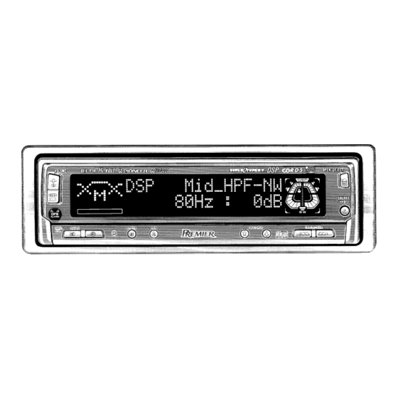
Page 117: Display
DEX-P1R,DEH-P946,DEX-P1 7.1.2 DISPLAY - CAW1470 (DEX-P1R/UC) - Page 118 DEX-P1R,DEH-P946,DEX-P1 - CAW1471 (DEH-P946/ES,DEX-P1/ES)
-
Page 119: Diagnosis
DEX-P1R,DEH-P946,DEX-P1 7.2 DIAGNOSIS 7.2.1 DISASSEMBLY - Removing the Case,Panel and - Removing the Panel Assy 1. A × 2 CD Mechanism Module 2. B × 2 1. A × 1 3. Connector × 4 2. Stopper × 5 4. Stopper × 2 3. -
Page 120: Test Mode
DEX-P1R,DEH-P946,DEX-P1 7.2.2 TEST MODE - Error Number Indication The system enters error mode to display the cause of error with a number when the system cannot operate CD or stops operation because of an error. The purpose of this measure is to reduce frequency of calls from users asking help for problems that are caused by incorrect operation by user, as well as to assist analysis and repair in servicing. - Page 121 DEX-P1R,DEH-P946,DEX-P1 - New Test Mode When S-CD is specified as the source, basically the system plays as normal operation. After setup, the system dis- plays the cause and time (absolute time) of an error if focus search is improper, spindle lock is removed, subcode cannot be read, or sound is skipped.
- Page 122 DEX-P1R,DEH-P946,DEX-P1 - S-MD Test Mode This mode is used by service personnel to solve problems when the mechanism is malfunctioned. Normally users do not enter S-MD Test mode. (1) Test mode input 1) How to input Input in the same manner as with inputting in Test mode of CDS, CDM, etc.
- Page 123 DEX-P1R,DEH-P946,DEX-P1 - SYSTEM Test Mode Function Operation Key · Trigger Remarks Display Display Set Acc to ON or connect the detach grille, Immediately after All LCDs light up. while pressing the S/A and → keys simultaneously. Test Mode resetting the system Then, press the S/A and →...
-
Page 124: Block Diagram
DEX-P1R,DEH-P946,DEX-P1 7.3 BLOCK DIAGRAM - DEX-P1R/UC TUNER AMP UNIT ASL UNIT Q4501 VR4501 ASL AMP ASL FILTER MIC4501 CN141 IC4501 IC4502 NOISE CN222 CN3001 NJM2068 NJM2068 CN451 CD DATA MAIN LRCK BICK FM / AM TUNER UNIT 26 25 Q31 CF51... - Page 125 DEX-P1R,DEH-P946,DEX-P1 DSP UNIT HIGH OUT PCB CN4153 CN231 IC4151 FRONT Lch SWITCH SWITCH CN3001 NJM4580 CN3001 Q4151 CD DATA Q231 IC3142 BICK LRCK TC7S08FU IC4251 REAR Lch LRCK BICK IC3141 NJM4580 BU4066BCFV Q232 Q4251 9 10 IC4351 A OUT L1 SUB.W Lch...
-
Page 126: Operations And Specifications
DEX-P1R,DEH-P946,DEX-P1 8. OPERATIONS AND SPECIFICATIONS 8.1 OPERATIONS... - Page 127 DEX-P1R,DEH-P946,DEX-P1...
- Page 128 DEX-P1R,DEH-P946,DEX-P1...
-
Page 129: Head Unit
DEX-P1R,DEH-P946,DEX-P1 Key Finder Head Unit OPEN/EJECT button +/– button SOURCE/OFF button [/] button S/A button FS button CLOCK button DISPLAY button button Remote Controller Buttons 1– 6 +/– button RT button DSP button [/] button '/ button BAND button DISPLAY button... - Page 130 DEX-P1R,DEH-P946,DEX-P1...
- Page 131 DEX-P1R,DEH-P946,DEX-P1...
- Page 132 DEX-P1R,DEH-P946,DEX-P1...
- Page 133 DEX-P1R,DEH-P946,DEX-P1...
- Page 134 DEX-P1R,DEH-P946,DEX-P1...
- Page 135 DEX-P1R,DEH-P946,DEX-P1...
- Page 136 DEX-P1R,DEH-P946,DEX-P1...
- Page 137 DEX-P1R,DEH-P946,DEX-P1...
- Page 138 DEX-P1R,DEH-P946,DEX-P1...
- Page 139 DEX-P1R,DEH-P946,DEX-P1...
- Page 140 DEX-P1R,DEH-P946,DEX-P1...
- Page 141 DEX-P1R,DEH-P946,DEX-P1...
- Page 142 DEX-P1R,DEH-P946,DEX-P1...
Need help?
Do you have a question about the DEX-P1R and is the answer not in the manual?
Questions and answers