Table of Contents
Advertisement
SERVICE MANUAL
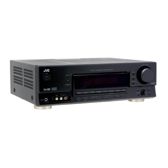
AUDIO/VIDEO CONTROL RECEIVER
2
2006
MB504
RX-5060BJ,RX-5060BC,
RX-5060BE,RX-5062SB,
RX-5062SE,RX-5062SEN,
Lead free solder used in the board (material : Sn-Ag-Cu, melting point : 219 Centigrade)
1
PRECAUTION. . . . . . . . . . . . . . . . . . . . . . . . . . . . . . . . . . . . . . . . . . . . . . . . . . . . . . . . . . . . . . . . . . . . . . . . . 1-4
2
Specific Service Instructions . . . . . . . . . . . . . . . . . . . . . . . . . . . . . . . . . . . . . . . . . . . . . . . . . . . . . . 1-6
3
Disassembly . . . . . . . . . . . . . . . . . . . . . . . . . . . . . . . . . . . . . . . . . . . . . . . . . . . . . . . . . . . . . . . . . . . . . . . 1-7
4
Adjustment . . . . . . . . . . . . . . . . . . . . . . . . . . . . . . . . . . . . . . . . . . . . . . . . . . . . . . . . . . . . . . . . . . . . . . . 1-13
5
Troubleshooting . . . . . . . . . . . . . . . . . . . . . . . . . . . . . . . . . . . . . . . . . . . . . . . . . . . . . . . . . . . . . . . . . 1-13
RX-5062SEV
TABLE OF CONTENTS
COPYRIGHT © 2006 Victor Company of Japan, Limited
TA/NEWS/INFO
DISPLAY MODE
No.MB504
2006/2
Advertisement
Table of Contents

Related Manuals for JVC RX-5060BJ


Summary of Contents for JVC RX-5060BJ
- Page 1 SERVICE MANUAL AUDIO/VIDEO CONTROL RECEIVER MB504 2006 RX-5060BJ,RX-5060BC, RX-5060BE,RX-5062SB, RX-5062SE,RX-5062SEN, RX-5062SEV TA/NEWS/INFO DISPLAY MODE Lead free solder used in the board (material : Sn-Ag-Cu, melting point : 219 Centigrade) TABLE OF CONTENTS PRECAUTION............... . . 1-4 SPECIFIC SERVICE INSTRUCTIONS .
- Page 2 SPECIFICATION Northern america version Amplifier Ω Output Power Front channels 100 W per channel, min. RMS, driven into 8 , at 1 kHz with no more than 10% total harmonic distortion. Ω Center channel 100 W, min. RMS, driven into 8 , at 1 kHz with no more than 10% total harmon- ic distortion.
- Page 3 Europian version Amplifier Ω Output Power Front channels 100 W per channel, min. RMS, driven into 8 , at 1 kHz with no more than 10% total harmonic distortion. Ω Center channel 100 W, min. RMS, driven into 8 , at 1 kHz with no more than 10% total harmon- ic distortion.
-
Page 4: Precaution
SECTION 1 PRECAUTION Safety Precautions (1) This design of this product contains special hardware and voltmeter. many circuits and components specially for safety purpos- Move the resistor connection to each exposed metal es. For continued protection, no changes should be made part, particularly any exposed metal part having a return to the original design unless authorized in writing by the path to the chassis, and measure the AC voltage across... - Page 5 Importance administering point on the safety FW201 R201 CN251 FC221 FC271 FC231 FC261 FC232 FC262 FC222 FC272 FC211 FC212 TA202 TA201 B107 PW102 B108 B101 B105 B110 PW101 PW105 PW103 B109 B102 B106 PW104 Full Fuse Replacement Marking Marquage Pour Le Remplacement Complet De Fusible Graphic symbol mark Le symbole graphique (Ce symbole signifie...
-
Page 6: Specific Service Instructions
SECTION 2 SPECIFIC SERVICE INSTRUCTIONS This service manual does not describe SPECIFIC SERVICE INSTRUCTIONS. 1-6 (No.MB504) -
Page 7: Disassembly
SECTION 3 DISASSEMBLY Main body 3.1.1 Removing the top cover (See Fig. 1 and 2) (1) Remove the three screws A attaching the top cover. (2) Remove the four screws B attaching the both side of top cover. Fig.1 Fig.2 (No.MB504)1-7... - Page 8 3.1.2 Removing the front panel assembly (See Fig. 3 to 5) (1) Remove the three screws C attaching the top side of front panel assembly. (2) Remove the four screws D attaching the bottom side of front panel assembly. (3) Remove the one screw E attaching the ground wire to front chassis.
- Page 9 3.1.3 Removing the rear panel and each I/O boards (See Fig. 6 to 8) (1) Remove the two screws F attaching the tuner board. (2) Disconnect the card wire from CN411 of main board. (3) Remove the three screws G attaching the digital board. (4) Disconnect the connector CN481 CN482...
- Page 10 3.1.4 Removing the main board (See Fig. 9) (1) Disconnect the connector CN471, CN472 CN473 from front board. (2) Disconnect the connection board from CN291 of regulator board and CN491 of main board. (3) Remove the two screws Q and one screw R attaching the Regulator board main board.
- Page 11 3.1.6 Removing the power transformer and regulator board (See Fig. 11 and 12) (1) Remove the four screws U attaching the power transform- (2) Remove the one screw V attaching the fuse board. (3) Remove the three screws W and one screw X attaching the regulator board.
- Page 12 Front panel assembly 3.2.1 Removing the micon board (See Fig. 14 and 16) (1) Take out the volume knob from front panel assembly. Volume knob (2) Remove the nut Z attaching the volume. (3) Remove the nine screws AA attaching the micon board. 3.2.2 Removing the power switch board (See Fig.
-
Page 13: Adjustment
SECTION 4 ADJUSTMENT This service manual does not describe ADJUSTMENT. SECTION 5 TROUBLESHOOTING This service manual does not describe TROUBLESHOOTING. (No.MB504)1-13... - Page 14 Victor Company of Japan, Limited Audio/Video Systems Category 10-1,1chome,Ohwatari-machi,Maebashi-city,371-8543,Japan (No.MB504) Printed in Japan...
- Page 15 SCHEMATIC DIAGRAMS AUDIO/VIDEO CONTROL RECEIVER RX-5060BJ,RX-5060BC,RX-5060BE RX-5062SB,RX-5062SE,RX-5062SEN RX-5062SEV CD-ROM No.SML200602 TA/NEWS/INFO DISPLAY MODE Lead free solder used in the board (material : Sn-Ag-Cu, melting point : 219 Centigrade) Contents Block diagrams Standard schematic diagrams 2-15 to 21 Printed circuit boards No.MB504SCH...
- Page 16 In regard with component parts appearing on the silk-screen printed side (parts side) of the PWB diagrams, the parts that are printed over with black such as the resistor ( ), diode ( ) and ICP ( ) or identified by the " " mark nearby are critical for safety.
- Page 17 < M E M O >...
-
Page 18: Block Diagram
Block diagram Audio/Video signal input Audio/Video Tuner Volume / Regulator / So terminal section (Video) signal input terminal For J/C TU_DATAIN section (DVD) COMPULINK TU_DATAOUT COMPULINK TU_CLK TU_CE SW_OUT SW_OUT For B/E/EN/EV VIDEO1 RDS_CLK MONITOR VIDEO2 RDS_DATA SW_OUT RDS_ONOFF IC501 DVD_L/R DVD_L/R SELECTOR... - Page 19 gulator / Source select IC section Audio amp section Audio amp section (Speaker terminal) S_MUTE Q1413 Q1420 IC101 ST301 U_DATAIN Q1414 U_DATAOUT L/Rch FR/FL U_CLK POWER RY302 U_CE E/EN/EV FRONT_A Q1417 IC102 CENTER CENTER RY303 ONOFF C/SL/SRch SURR L Q1418 POWER SURR R CENTER...
- Page 20 Standard schematic diagrams Primary section LVA10652-3 LVA10652-4 L V A 1 0 6 5 2 - 1 L V A 1 0 6 5 2 - 2 J / C P O W E R T R A N S F O R M E R B / E / E T 2 0 1 Q Q T 0 5 1 8 - 0 0 1...
- Page 21 LVA10652-3 LVA10652-4 L V A 1 0 6 5 2 - 1 L V A 1 0 6 5 2 - 2 POWER TRANSFORMER B / E / E N / E V T 2 0 1 QQT0518-002 P W 3 1 1 1 1 4 0 1 4 P W 1 0 1...
- Page 22 Audio amp section f r o m C N 4 7 1 ( L V A 1 0 6 5 4 - 1 ) C N 1 7 1 P W 6 0 1 Q J P 0 0 1 - 0 3 1 8 0 1 - E I C 1 0 1 I C 1 0 2 L V A 1 0 6 5 3 - 1...
- Page 23 f r o m C N 4 7 2 f r o m C N 4 7 3 ( L V A 1 0 6 5 4 - 1 ) ( L V A 1 0 6 5 4 - 1 ) Q J P 0 0 2 - 0 2 1 2 0 1 - E C N 2 7 2 P W 6 0 2...
- Page 24 Volume / Regulator / Source selector section J / C B / E / E N / E V U S / U N / U T / U P t o C N 4 0 1 ( A U D I O ) t o C N 6 8 3 ( D S P ) t o C N 6 8 1...
- Page 25 C N 6 8 1 ( D S P ) V A 1 0 4 7 0 ) t o C N 7 0 2 ( F R O N T ) ( L V A 1 0 6 5 4 - 2 ) C N 4 0 2 CN482 Q G F 1 2 0 5 C 2 - 2 7...
- Page 26 Audio, Video signal control / Souce selector section L V A 1 0 6 5 3 - 3 A U D I O I N P U T / O U T P U T C 4 4 3 R 4 7 1 R 4 7 2 C 4 2 0 4 7 / 2 5...
- Page 27 L V A 1 0 6 5 3 - 5 C 4 4 3 4 7 / 2 5 C N 4 0 4 Q G A 2 5 0 1 F 1 - 0 3 D V D B 1 0 1 1 C 4 3 7 A U X _ L A U X _ L...
- Page 28 Surround / DSP section 1 2 . 9 V R 2 0 0 7 1 2 . 9 V 2 2 K C 2 0 1 3 R 2 0 2 2 3 3 0 L I N - 3 3 P C 2 0 0 9 T P _ 1 1 0 .
- Page 29 T P _ 1 K 2 8 6 1 R 2 8 6 1 D I G I T A L I N 1 2 2 0 N Q R 0 2 6 9 - 0 0 4 X R X 0 J 6 8 1 Q N N 0 4 8 1 - 0 0 1 C 2 8 8 1...
- Page 30 User control key / System control LSI / FL display section L V A 1 0 6 5 4 - 2 C 7 0 9 4 . 7 / 5 0 R A 7 0 1 N . I . D I 7 0 1 Q L F 0 1 3 2 - 0 0 1 - - - - -...
- Page 31 C 7 0 7 4 . 7 / 5 0 R A 7 0 1 N . I . G R I D 1 - 1 2 . 0 V Q 7 0 7 K R C 1 0 7 S - X C N 7 0 5 5 .
-
Page 32: Printed Circuit Boards
Printed circuit boards Power supply board Lead free solder used in the board (material : Sn-Ag-Cu, melting point : 219 Centigrade) (Relay board) (Video board) CN501 R507 C511 R508 C512 C504 C515 Q503 R505 R506 R512 Q502 C513 R501 C501 R502 C507 R509... - Page 33 (Power transformer board 1) FW201 CN251 R201 FC221 FC271 FC261 FC231 FC222 FC272 FC262 FC232 (Main board) FW201 PW203 C201 RY202 C203 C202 PW204 PW205 D204 CN291 D202 C209 CN203 R203 R204 C218 D220 D221 Q210 Q203 D218 D217 C213 D212 R209 Q205...
- Page 34 Amp board Lead free solder used in the board (material : Sn-Ag-Cu, melting point : 219 Centigrade) (DVD board) J404 J406 C452 C460 R452 R482 Q451 R456 C465 R457 R458 IC451 CN452 R460 R461 C468 (Speaker terminal board) FW303 FW301 R1270 FW302 D1353...
- Page 35 (Audio board) R435 R410 R409 R477 C402 C401 R436 R478 CN401 R429 R447 R475 C444 R448 R430 R446 R476 R445 R431 C433 C443 R408 R407 C434 Q403 R432 R423 R473 Q404 IC401 R474 R424 R425 R406 C427 R405 Q401 C438 C437 C428 R479...
- Page 36 Front board Lead free solder used in the board (material : Sn-Ag-Cu, melting point : 219 Centigrade) S722 S721 R723 R722 R721 R725 R724 R733 S732 S731 S724 S723 (System control board) R737 R736 S738 R741 S734 S735 S757 S736 S756 S740 R740...
- Page 37 S750 S745 R725 R724 R726 R727 S723 S725 S726 R778 S743 R746 S742 S757 S737 S739 S741 JS702 R742 R747 R745 CN706 R743 R799 R795 R798 R797 R796 R708 R768 R720 R713 R712 R709 IC704 S751 R783 R784 R785 R786 R788 R787 R791...
- Page 38 DSP board Lead free solder used in the board (material : Sn-Ag-Cu, melting point : 219 Centigrade) forward side C2955 R2185 IC691 C2952 R2189 Q2710 R2191 Q2708 R2773 C2183 IC615 C2911 C2901 C2924 C2922 CN681 R2147 R2145 R2133 R2137 R2103 R2128 C2115 R2706...
- Page 39 < M E M O >...
- Page 40 Victor Company of Japan, Limited Audio/Video Systems Category 10-1,1chome,Ohwatari-machi,Maebashi-city,371-8543,Japan Printed in Japan (No.MB504SCH)
-
Page 41: Parts List
PARTS LIST RX-5060BJ,RX-5060BC,RX-5060BE RX-5062SB,RX-5062SE,RX-5062SEN,RX-5062SEV * All printed circuit boards and its assemblies are not available as service parts. - Contents - Exploded view of general assembly and parts list (Block No.M1) Electrical parts list (Block No.01~04) 3-16 Packing materials and accessories parts list (Block No.M3) - Page 42 Exploded view of general assembly and parts list Block No. Power transformer board Power transformer board F207 F206 F203 Power/Fu F202 F205 Headphone jack board Main board Power switch board BK701 BK702 System control board...
- Page 43 Speaker terminal board ansformer F201 Power/Fuse board Relay board 74 73 Front board Power amp. board Wire protection board...
- Page 44 Symbol No. Part No. Part Name Description Local LV10756-033A FRONT PANEL 5060BJ,5060BC LV10756-034A FRONT PANEL 5060BE LV10756-036A FRONT PANEL 5062SE,5062SB,5062SEN,5062SEV LV43338-002A JVC MARK LV34003-001A LENS LV34000-003A PUSH BUTTON(POW 5060BJ,5060BC,5060BE LV34000-004A PUSH BUTTON(POW 5062SE,5062SB,5062SEN,5062SEV LV42096-001A INDICATOR LV21420-003A PUSH BUTTON 5060BJ,5060BC,5060BE LV21420-004A...
- Page 45 Symbol No. Part No. Part Name Description Local LV30225-0H3A SPACER (x2) LV21649-005A TOP COVER 5060BJ,5060BC,5060BE LV21649-006A TOP COVER 5062SE,5062SB,5062SEN,5062SEV QYSBSGY3008EA TAP SCREW M3 x 8mm(x3) E406308-006 SPECIAL SCREW (x4) 5060BJ,5060BC,5060BE E406308-007 SPECIAL SCREW (x4) 5062SE,5062SB,5062SEN,5062SEV LV43463-001A VOL KNOB ASSY 5060BJ,5060BC,5060BE LV43463-002A VOL KNO ASSY...
- Page 46 Electrical parts list Main board Symbol No. Part No. Part Name Description Local Block No. [0][1] C901 QCSB1HJ-470Y C CAPACITOR 47pF 50V J Symbol No. Part No. Part Name Description Local C903 QCBB1HK-331Y C CAPACITOR 330pF 50V K C904 QCBB1HK-331Y C CAPACITOR...
-
Page 47: Amplifier Board
Symbol No. Part No. Part Name Description Local Symbol No. Part No. Part Name Description Local FC272 QNG0020-001Z FUSE CLIP I.M 5060BE, 5062SE, FW201 QUM215-14Z3Z3-E PARA RIBON WIRE 5062SB, C421 QCBB1HK-331Y C CAPACITOR 330pF 50V K FW251 QUM213-08DGZ3-E PARA RIBON WIRE 5062SE N,5062S... - Page 48 Symbol No. Part No. Part Name Description Local Symbol No. Part No. Part Name Description Local C1111 QEZ0806-688 E CAPACITOR 6800uF 5060BE, 5062SE, C1112 QEZ0806-688 E CAPACITOR 6800uF 5062SB, C1365 QFLC1HJ-473Z M CAPACITOR 0.047uF 50V J C1113 QEZ0805-478 E CAPACITER 4700uF 5062SE...
- Page 49 Symbol No. Part No. Part Name Description Local Symbol No. Part No. Part Name Description Local R472 QRE141J-473Y C RESISTOR 47kΩ 1/4W J R1235 QRJ146J-2R2X UNF C RESISTOR 2.2Ω 1/4W J R473 QRE141J-473Y C RESISTOR 47kΩ 1/4W J ...
-
Page 50: Front Board
TRANSISTOR C1403 QETN1EM-107Z E CAPACITOR 100uF 25V M Q1408 KTA1271/OY/-T TRANSISTOR C1404 QETN1EM-107Z E CAPACITOR 100uF 25V M Q1413 2SC3576-JVC-T TRANSISTOR C1405 QETN1EM-107Z E CAPACITOR 100uF 25V M Q1414 2SC3576-JVC-T TRANSISTOR C1406 QETN1CM-108Z E CAPACITOR 1000uF 16V M Q1417... - Page 51 Symbol No. Part No. Part Name Description Local Symbol No. Part No. Part Name Description Local R701 NRSA63J-472X MG RESISTOR 4.7kΩ 1/16W J R783 NRSA63J-221X MG RESISTOR 220Ω 1/16W J R702 NRSA63J-223X MG RESISTOR 22kΩ 1/16W J R784 NRSA63J-221X MG RESISTOR 220Ω...
-
Page 52: Dsp Board
Symbol No. Part No. Part Name Description Local Symbol No. Part No. Part Name Description Local R1462 QRJ146J-2R2X UNF C RESISTOR 2.2Ω 1/4W J S740 QSW0683-001Z PUSH SW I.M R1464 NRSA63J-104X MG RESISTOR 100kΩ 1/16W J S741 QSW0683-001Z PUSH SW I.M R1470... - Page 53 Symbol No. Part No. Part Name Description Local Symbol No. Part No. Part Name Description Local C2112 NCF31CZ-104X C CAPACITOR 0.1uF 16V Z C2641 NDC31HJ-100X C CAPACITOR 10pF 50V J C2113 NCB31HK-331X C CAPACITOR 330pF 50V K C2642 NDC31HJ-100X C CAPACITOR 10pF 50V J...
- Page 54 Symbol No. Part No. Part Name Description Local Symbol No. Part No. Part Name Description Local R2109 NRSA63J-104X MG RESISTOR 100kΩ 1/16W J R2387 NRSA63J-181X MG RESISTOR 180Ω 1/16W J R2110 NRSA63J-104X MG RESISTOR 100kΩ 1/16W J R2389 NRSA63J-562X MG RESISTOR 5.6kΩ...
- Page 55 Symbol No. Part No. Part Name Description Local R2726 NRSA63J-822X MG RESISTOR 8.2kΩ 1/16W J R2727 NRSA63J-432X MG RESISTOR 4.3kΩ 1/16W J R2728 NRSA63J-221X MG RESISTOR 220Ω 1/16W J R2731 NRSA63J-221X MG RESISTOR 220Ω 1/16W J R2732 NRSA63J-221X MG RESISTOR 220Ω...
- Page 56 Packing materials and accessories parts list Block No. No additional / supplemental order of WARRANTY CARDs are available <RX-5060BJ> <RX-5060BJ><RX-5060BC> <RX-5060BE> <RX-5062SE> A1,A4,A5, <RX-5062SEN> A6,A8, <RX-5062SEV> <RX-5060BC> A1,A4,A5, A6,A7, <RX-5060BE> <RX-5062SE> <RX-5062SB> <RX-5062SEN> <RX-5062SEV> A1,A2,A4, A5,A6, A1,A4,A5,A6, A7,A8 3-16...
- Page 57 Packing and Accessories Block No. [M][3][M][M] Symbol No. Part No. Part Name Description Local LVT1507-001A INST BOOK 5060BJ LVT1507-002A INST BOOK ENG FRE 5060BC LVT1507-004A INST BOOK GER FRE 5060BE,5062SE LVT1507-003A INST BOOK 5062SB LVT1507-006A INST BOOK SPA POL 5062SEN LVT1507-008A INST BOOK...
Need help?
Do you have a question about the RX-5060BJ and is the answer not in the manual?
Questions and answers