Zenith XBS344 Series Service Manual
Combo home theater system
Hide thumbs
Also See for XBS344 Series:
- Installation and operating manual (48 pages) ,
- Installation and operating manual (48 pages)
Table of Contents
Advertisement
Quick Links
SERVICE MANUAL
Product Type: Combo Home Theater System
Chassis: D35 (DECK), DP-7C (MD)
Manual Series: XBS344(DT-66550M)
Manual Part #: 3829RGN002Q
Model Line: F
Product Year: 2003
CONTENTS
....................................................
Summary
Cabinet & Main Chassis
.....................................................
Electrical
........................................
VCR Mechanism
........................................
DVD Mechanism
....................................................
Parts List
Published August 2003
by Technical Publications
Zenith Electronics Corporation
201 James Record Road
Huntsville, Alabama 35824-1513
Copyright © 2003 by Zenith Electronics Corporation
1
1
.............................
2
3
4
5
6
Model Series:
XBS344
(DT-66550M)
Advertisement
Chapters
Table of Contents
Troubleshooting

Related Manuals for Zenith XBS344 Series


Summary of Contents for Zenith XBS344 Series
- Page 1 Summary ......Cabinet & Main Chassis ............. Electrical ........VCR Mechanism ........DVD Mechanism ............ Parts List Published August 2003 by Technical Publications Zenith Electronics Corporation 201 James Record Road Huntsville, Alabama 35824-1513 Copyright © 2003 by Zenith Electronics Corporation...
- Page 3 CONTENTS SECTION 1 ..SUMMARY SECTION 2 ..CABINET & MAIN CHASSIS SECTION 3 ..ELECTRICAL SECTION 4 ..MECHANISM OF VCR PART SECTION 5 ..MECHANISM OF DVD PART SECTION 6 .
-
Page 4: Table Of Contents
SECTION 1 SUMMARY CONTENTS PRODUCT SAFETY SERVICING GUIDELINES FOR VIDEO PRODUCTS ..... 1-2 SERVICING PRECAUTIONS ....................1-3 • General Servicing Precautions • Insulation Checking Prodedure • Electrostatically Sensitive Devices SPECIFICATIONS ........................1-4... -
Page 5: Product Safety Servicing Guidelines For Video Products
When servicing this product, under no circumstances should the original design be modified or altered without permission from Zenith Electronics Corporation. All components should be replaced only with types identical to those in the original circuit and their physical location, wiring and lead dress must conform to original layout upon completion of repairs. -
Page 6: Servicing Precautions
SERVICING PRECAUTIONS CAUTION: Before servicing the COMBO HOME THEATER Electrostatically Sensitive (ES) Devices SYSTEM covered by this service data and its supplements Some semiconductor (solid state) devices can be damaged and addends, read and follow the SAFETY PRECAUTIONS. easily by static electricity. Such components commonly are NOTE: if unforeseen circumstances create conflict between called Electrostatically Sensitive (ES) Devices. -
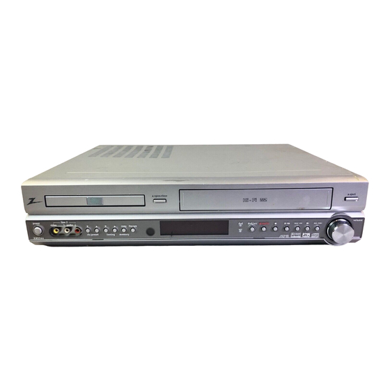
Page 7: Specifications
Net Dimensions (W x H x D) 100 x 147 x 127.5 mm 200 x 425 x 381 mm (3.9 x 5.8 x 5.0 inches) (7.9 x 16.7 x 15 inches) Net Weight 0.92 kg (2.0 lbs) 7.06kg (15.6 lbs) FRONT VIEW (XBS344) - Page 8 SECTION 2 CABINET & MAIN CHASSIS CONTENTS 1. EXPLODED VIEWS ........................2-2 1. Cabinet and Main Frame Section ...................2-2 2. Woofer Speaker Section (DTE-5105WE)................2-3 3. Speaker Section (DTE-550TE) ....................2-4 4. Packing Accessory Section ....................2-5...
-
Page 9: Exploded Views
EXPLODED VIEWS 1. Cabinet and Main Frame Section... -
Page 10: Woofer Speaker Section (Dte-5105We)
2. Woofer Speaker Section (DTE-5105WE) -
Page 11: Speaker Section (Dte-550Te)
3. Speaker Section (DTE-550TE) 851A... -
Page 12: Packing Accessory Section
4. Packing Accessory Section CABLE SET ASS'Y, RF PLUG ASS'Y 1WAY(YELLOW) CABLE, COAXIAL PLUG ASS'Y 2WAY CABLE, DIN 820 PLUG ASS'Y 1WAY(BLACK) BATTERY OWNER'S MANUAL REMOCON PACKING, CASING 803A PACKING, CASING 803B 803C PACKING, CASING SHEET PACKING, CASING OPTIONAL PARTS... - Page 13 SECTION 3 ELECTRICAL CONTENTS OVERALL WIRING DIAGRAM DVD & AMP PART ......3-2 VCR PART ELECTRICAL TROUBLESHOOTING GUIDE ................3-56 ELECTRICAL ADJUSTMENT 1. SYSTEM OPERATION FLOW......3-56 2. TEST & DEBUG FLOW........3-57 PROCEDURES ............3-3 3. AUDIO µ-COM CIRCUIT(DVD & AMP)....3-63 ELECTRICAL TROUBLESHOOTING DETAILS AND WAVEFORMS ON GUIDE ................3-4 SYSTEM TEST AND DEBUGGING...
-
Page 14: Overall Wiring Diagram
OVERALL WIRING DIAGRAM... -
Page 15: Vcr Part
VCR PART ELECTRICAL ADJUSTMENT PROCEDURES 1. Servo Adjustment 1) PG Adjustment • Test Equipment a) OSCILLOSCOPE b) NTSC MODEL : NTSC SP TEST TAPE • Adjustment And Specification MODE MEASUREMENT POINT ADJUSTMENT POINT SPECIFICATION V.Out PLAY R/C TRK JIG KEY 6.5 ±... -
Page 16: Electrical Troubleshooting Guide
ELECTRICAL TROUBLESHOOTING GUIDE 1. Power(SMPS) CIRCUIT (1) No 5.3VA (SYS/Hi-Fi/TUNER) (2) No 12VA (TO CAP, DRUM MOTOR) NO 5.3VA. NO 12VA. Replace the F101. Is the Vcc(13V) supplied Check or Replace Is the F101 normal? (Use the same Fuse) to (+) terminal in D115? the D110. - Page 17 (4) No 5V (TO DVD) (5) No 33V (TUNER) NO 5V. No 33V. Is 5.3VA put into Check the Power 5.3VA Line Check. Is Q163 Base “H”? the Q160 Emitter? Control. Is the Q162 Base Check the Power Check or Replace “H”? Control.
-
Page 18: System/Key Circuit
2. SYSTEM/KEY CIRCUIT (1) AUTO STOP Auto Stop Does the SW30 waveform Check the Drum Motor appear at the IC501 signal. Pin18? Do T/UP Reel Pulses Do the T-UP Reel Pulses Does 5V appear at the appear at the point appear at the IC501 Pin80? RS501? between R556 and R536? -
Page 19: Servo Circuit
3. SERVO CIRCUIT (1) Unstable Video in PB MODE Unstable Video in PB Mode. Does the Noise level of the screen change periodically? Do the CTL pulses appear Is adjusting the height of at the IC501 Pin97? the CTL Head accurate? Does the CFG waveform Readjust the height of the appear at the IC501... - Page 20 2. SERVO CIRCUIT (3) When the Capstan Motor doesn’t run, When the Capstan Motor doesn’t run, Refer to “SMPS(CAPSTAN/12Volt) Does 12VA appear at the PMC01? Trouble Shooting”. Is “DRUM CTL” 2.8V appear at the PMC01? Check the PMC01 and the Capstan Does the PWM signal appear at the Motor Ass’y.
-
Page 21: Osd Circuit
2. SERVO CIRCUIT (4) KEY doesn’t working KEY doesn’t working. Is 5V applied to the IC501 Refer to “SMPS 5.3VA Pin79? Trouble Shooting”. Does LED or FLD change Replace the defective when a function button is switches. pressed? 4. OSD CIRCUIT (1) No OSD display. -
Page 22: Y/C Circuit
5. Y/C CIRCUIT (1) No Video in EE Mode, No Video in EE Mode Does the Video signal Does the Video signal Check DVD Video Input appear at the IC301 appear at the IC302 (IC602, Pin4), Tuner Video Pins28, 30, 32? Pins1, 5? Input (TU701 Pin16), Line Video Input (JK601),... - Page 23 3. Y/C CIRCUIT (2) When the Y(Luminance) signal doesn’t appear on the screen in PB Mode, Is 5V applied to the IC301 Check the line of the REG Pins23, 44, 45, 52, 68, 77? 5V Line. (Power Circuit) Is the Y/C Bus siganl Refer to ‘SYSTEM Y/C applied to the IC301 BUS CHECK Trouble...
- Page 24 3. Y/C CIRCUIT (3) When the C(Color) signal doesn’t appear on the screen in PB Mode, Is 5V applied to the IC301 Check the line of the REG Pins23, 44, 45, 52, 68, 77? 5V Line. (Power Circuit) Is normal the X301 Does the fsc signal appear (3.58MHZ) of oscillation Replace the X301.
- Page 25 3. Y/C CIRCUIT (4) When the Video signal doesn’t appear on the screen in REC Mode, REC mode Is EE mode normal? Check the EE mode Is brightness normal? Is color normal? Is the brightness signal sup- Does signal appear at Check X301 oscillation IC301 Pins41, 50? frequency.
-
Page 26: Tuner/If Circuit
6. Tuner/IF CIRCUIT (1) No Picture on the TV screen No picture on the TV screen Does the Video signal at Is +33V applied to TU701 Check 33V line. the TU701 Pin16. Pin14? Is +5V applied to TU701 Check 5V line. Pin3? Does the Clock signal Check the lIC Clock Signal... - Page 27 (2) No Sound No Sound. Check the Vcc of TU701 Pins3, 14. Check 5.2V, 33V Line. Check the Tuner SiF signal at IC801 Check the Tuner SIF of TU701 Pin13. Pin57. 1. Check the Vcc(5.3VA, 9V) of IC801 Check the Audio of IC801 Pins78, 80. Pins3, 5, 36, 54.
-
Page 28: Hi-Fi Circuit
7. Hi-Fi Circuit Hi-Fi Playback. Check the Vcc of IC801. No sound (Pins 3, 15, 32, 46) Check the Hi-Fi Selection Check power. Switch and the Tape quality. Is the RF waveform at IC801 Pin 23 over 3V Vp-p? Is Pin 30 of IC801 over Check REC start “H”... - Page 29 Hi-Fi REC. It is impossible to record and playback Hi-Fi Audio signal. Check Vcc of IC801. (Pins 3, 15, 32, 46) Check IC801 Pin 37(Data),Pin 38(CLOCK). Check Power. Is IC501 Pin 84(A.Mute) “High”? Check ports of µ-COM. Are Audio signals present at IC801 Check the Port of µ-COM.
-
Page 30: Block Diagrams
BLOCK DIAGRAMS 1. POWER(SMPS) BLOCK DIAGRAM 1 PSW01 T101 BD101 32VA BD101 RECTIFER & SMOOTHING 12VA BLOCK C103 12V REG PWR SENSE BLOCK ( D122, C131, R131, C132, C133, C135, L122 ) ( IC153, C139 ) DRIVE & S/W BLOCK QUASI-RESONANT BLOCK ( IC101, R114, R115, C123, C107, BC101, D108, R101, D102, R102,... - Page 31 2. POWER(SMPS) BLOCK DIAGRAM 2 TO SYS FD(+) TO SYS FD(-) TO SYS -29VA 12VT BLOCK (IC164, C162, R171) 33VT BLOCK TO TU (Q163, R168, 33VT R169, R170) TO TU REG 12VT PVD01 8V BLOCK FD(+) 5.3VA (IC160, D163, C163, R161) FD(-) -29VA REG 12VT...
-
Page 32: Jack & Tuner Block Diagram
3. JACK & TUNER BLOCK DIAGRAM C871 4.7µ/50V IC801 C711 C712 1500p TU701 R710 R711 A.IN 1.0K R706 MOD CTL MOD CTL 10µM R708 5.0V 5.0V R702 VCR'H' VCR'H' 1.0K A.IN V.IN MOD VIDEO CH S/W C702 C703 C708 PVT01 PVT01 220µ/6.3V 10.1µF... -
Page 33: Y/C Block Diagram
4. Y/C BLOCK DIAGRAM (PB Mode) (REC Mode) 55 54 53 51 50 49 48 47 55 54 53 320FH SERIAL VX01 AUDIO C-ROT DECODER MUTE RF-SW HA SW CLAMP CLAMP EP PB 'A' EP REC CLAMP EP PB 'B' CLAMP IC302 3.58M... -
Page 34: Normal Audio Block Diagram
5. NORMAL AUDIO BLOCK DIAGRAM 1) EE Mode 2) PB Mode 3) REC Mode DT-65780M's 3-26 3-27... -
Page 35: Hi-Fi Block Diagram
6. Hi-Fi BLOCK DIAGRAM Hi-Fi/ AUDIO INPUT 26 27 BLOCK DEMO DULATE FM MODU A.OUT 'L' DE MODU DVD A.IN 'L' A.OUT DVD AUDIO A.OUT 'R' To JACK DVD A.IN 'R' AV1 A.IN 'L' INPUT REAR JACK OUTPUT SELECT AV1 A.IN 'R' SELECT MODULATOR AV2 A.IN 'L'... -
Page 36: System Block Diagram
7. SYSTEM BLOCK DIAGRAM TO/FROM DECK TO/FROM AVCP 5.3VA MODE S/W MS501 95 94 87 12 9 18 13 16 59 CV IN I-Limit COMP IN MODE S1 MODE S1 MODE S2 REC 'H' MODE S2 MODE S3 MODE S4 C.ROT MODE S3 A.MUTE'H'... -
Page 37: Circuit Diagrams
2. Voltages are DC-measured with a digital voltmeter MODIFIED OR ALTERED WITHOUT PERMISSION IMPLEMENTATION OF THE LATEST SAFETY AND during Play mode. FROM THE ZENITH ELECTRONICS CORPORATION. PERFORMANCE IMPROVEMENT CHANGES INTO ALL COMPONENTS SHOULD BE REPLACED ONLY THE SET IS NOT DELAYED UNTIL THE NEW SERVICE WITH TYPES IDENTICAL TO THOSE IN THE ORIGI- LITERATURE IS PRINTED. - Page 38 2. POWER(SMPS) CIRCUIT DIAGRAM 2 R171 4.7K SR13601A 3-34 3-35...
-
Page 39: Jack/Tuner Circuit Diagram
3. JACK, TUNER CIRCUIT DIAGRAM 03. 08. 15 SR13605A 3-36 3-37... -
Page 40: A/V Circuit Diagram
4. A/V CIRCUIT DIAGRAM IC301 Pins 53, 54, 55 are defective. IC301 doesn’t operate. X301 is defective. IC301 Pin 57 is defective. PB COLOR Signal disappear. PB COLOR Signal disappear. IC301 Pin 59 is defective. Auto Tracking is failed. Q306, Q307 are defective. EE, PB Screen doesn’t appear. - Page 41 5. Hi-Fi CIRCUIT DIAGRAM IC801 Pins37, 38 aredefective. All Audio is not appear. KTC3875 23 Pin is defective. Hi-Fi Audio is not appear. '02. 12. 04 R13604A 3-40 3-41...
-
Page 42: System Circuit Diagram
6. SYSTEM CIRCUIT DIAGRAM Just clock OSD is unstable. µ-COM will not operate. OSD will not operate. R597, C590, C589 are defective. X501, X502 are defective. L511, R598, C595, C596 are defective. Deck will not operate. R575, R576, R577, R578 are defective. µ-COM is unstable. -
Page 43: Key Circuit Diagram
7. KEY CIRCUIT DIAGRAM SR13610A 3-44 3-45... -
Page 44: Waveforms
• WAVEFORMS * IC301 Waveform * IC501 Waveform Stop : 10.0KS/s 280 Acqs Stop : 250KS/s 299 Acqs Stop : 10.0KS/s 18 Acqs Trigger Position: 12% Stop : 10.0KS/s 27 Acqs 1.00 V M 5.00ms 3.04 V 1.00 V M5.00ms 3.04 V 1.00 V M 200µs... -
Page 45: Circuit Voltage Chart
• CIRCUIT VOLTAGE CHART MODE MODE MODE MODE MODE MODE Base Emitter Collector Location PLAY PLAY PLAY PLAY PLAY PLAY PIN NO. PIN NO. PIN NO. PIN NO. PIN NO. PIN NO. I C 3 0 1 0.68 0.93 5.19 5.19 3.86 0.23... -
Page 46: Printed Circuit Diagrams
PRINTED CIRCUIT DIAGRAMS 1. MAIN P.C.BOARD LOCATION GUIDE 3-50 3-51... -
Page 47: Tuner P.c.board
2. TUNER P.C.BOARD 3. POWER P.C.BOARD LOCATION GUIDE 3-52 3-53... -
Page 48: Key 1(Left) P.c.board
4. KEY 1(LEFT) P.C.BOARD LOCATION GUIDE 5. KEY 2(RIGHT) P.C.BOARD LOCATION GUIDE 3-54 3-55... -
Page 50: Dvd & Amp Part
DVD & AMP PART ELECTRICAL TROUBLESHOOTING GUIDE 1. System operation flow Power On 1. 8032 initializes SERVO, DSP & RISC registers 2. Write RISC code to SDRAM 3. Reset RISC Show LOGO Tray Closed? Tray Close to Closed position SLED at Inner Side? SLED Moves to Inner Position 1. -
Page 51: Test & Debug Flow
2. Test & debug flow TEST Check the AC Vol tage Check the POWER PART Power PCBA (110V or 220V) Switch on the Power PCBA the DC Voltage outputs OK? Check the POWER PART (5V, 3.3V, 8V, 12V) Is 3.3V and 2.5V DC Check the regulators or diode(D501). - Page 52 RESET or Power On. Flash Check connection lines between FLASH Memory operates Show LOGO? & MT1379 and the FLASH access time properly? whether is sui table or not. SDRAM Check connection lines between SDRAM(IC502,IC503) & MT1379 and the works properl y? SDRAM is damaged.
- Page 53 Does the SLED move Check the connection line of Motor Driver STBY to inner side when it is at STBY signal . Pin is High? outer position? Check the related circuit of Motor Driver STBY FMSO. Pin is High? Check the amp circuit on SL+ and SL- output motor driver.
- Page 54 Check the laser power circuit Laser turns on when LD01 or LD02 output on MT1336 and connecting to reading disc? properly? power transistor. (Q404, Q405) Collector Check the related circuit on voltage of power transistor is OK? laser power transi stor (Q404, Q405) Check cable connection between transistor output and pick-up head.
- Page 55 Proper Check connections between signals on A, B, C, Focus ON OK? MT1336 and pick-up head. D of MT1336 Check the related circuit Proper FEO signal on MT1336 FEO sugnal . on MT1336? Check FEO connection between MT1336 and MT1379 Check the related Proper FEO signal Track On OK?
- Page 56 Audio Normal DAC received Check connection between MT1379 Audio output & Audio DAC. (Check ARCK, ALRCK correct data stream? when disc playback? ACKL, ASDAT3) Normal Check the related circuit of Audio DAC Audio DAC. (Check Audio out? (IC206) out Pins 8, 5) Check Audio filter, amplify, mute circuit.
-
Page 57: Audio Μ-Com Circuit(Dvd & Amp)
3. AUDIO µ-COM Circuit(DVD & AMP) POWER ON Does CD/DVD appear Does CD/DVD appear at FLT? at FLT? Does Loading appear Does it appear DVD Error at FLD? at FLD? Does no Dise or Time Check Connector (DVV01) Reconnet it. appear at FLD? if is normally. -
Page 58: Details And Waveforms On System Test And Debugging
DETAILS AND WAVEFORMS ON SYSTEM TEST AND DEBUGGING 1. SYSTEM 27MHz CLOCK,RESET,FLASH R/W SIGNAL 1) MT1379 main clock is at 27MHz(X501) 3.8V, 27MHz FIG 1-1 2) MT1379 & MT1336 reset is high active. Power Cord in 5.2VA PWR_CTL(SYSTEM µ-COM) IC501 PIN83) M_RESET(PDV03 PIN6) URST(IC501 PIN 188) FIG 1-2... - Page 59 3) RS232 waveform during procedure(Downloading) TXD(J501 PIN3) RXD(J501 PIN 2) FIG 1-3 4) Flash R/W enable signal during download(Downloading) FRD(IC5A1 PIN 28) FWR(IC5A1 PIN 11) FIG 1-4 3-65...
-
Page 60: Sdram Clock
2. SDRAM CLOCK 1) MT1379 main clock is at 27MHz(X501) DCLK = 93MHz, Vp-p=2.2, Vmax=2.7V (IC502,IC503 PIN 35) FIG 2-1 3. TRAY OPEN/CLOSE SIGNAL 1) Tray open/close waveform OPEN((PDM03 PIN7) CLOSE(PDM03 PIN8) TROPEN(IC402 PIN 1) TRCLOSE(IC402 PIN 2) FIG 3-1 3-66... - Page 61 2) Tray close waveform OPEN((PDM03 PIN7) CLOSE(PDM03 PIN8) TROPEN(IC402 PIN 1) TRCLOSE(IC402 PIN 2) FIG 3-2 3) Tray open waveform OPEN(PDM03 PIN7) CLOSE(PDM03 PIN8) TROPEN(IC402 PIN 1) TRCLOSE(IC402 PIN 2) FIG 3-3 3-67...
-
Page 62: Sled Control Related Signal (No Disc Condition)
4. SLED CONTROL RELATED SIGNAL (NO DISC CONDITION) FMSO(2.0V/1.4V/1.0V) (IC501 PIN 19) STBY(5V) – (IC401 PIN 50) SL+(4.7V/3.6V/1.9V) (IC402 PIN 12) SL-(5.3V/3.7V/2.5V) (IC402 PIN 13) FIG 4-1 5. LENS CONTROL RELATED SIGNAL(NO DISC CONDITION) FOSO(1.5V/1.4V/1.3V) (IC501 PIN 12) F+(4.0V/3.6V/3.2V) (IC402 PIN 9) F-(4.0V/3.6V/3.2V) (IC402 PIN 8) FIG 5-1... -
Page 63: Laser Power Control Related Signal(No Disc Condition)
6. LASER POWER CONTROL RELATED SIGNAL(NO DISC CONDITION) MDI1(0V/180mV) (IC401 PIN 124) LD01(5.0V//3.5V) IC401 PIN 125) LD02(5.0V/3.6V) (IC401 PIN 126) FIG 6-1 7. DISC TYPE JUDGEMENT WAVEFORMS F+(IC402 PIN 9) FE(IC401 PIN 18) RFL(IC401 PIN 19) FIG 7-1 (DVD) 3-69... - Page 64 F+(IC402 PIN 9) FE(IC401 PIN 18) RFL(IC401 PIN 19) FIG 7-2 (DVD) F+(IC402 PIN 9) FE(IC401 PIN 18) RFL(IC401 PIN 19) FIG 7-3 (CD) 3-70...
-
Page 65: Focus On Waveforms
F+(IC402 PIN 9) FE(IC401 PIN 18) RFL(IC401 PIN 19) FIG 7-4 (CD) 8. FOCUS ON WAVEFORMS FE(IC401 PIN 18) FOSO(IC501 PIN12) F+(IC402 PIN 9) F-(IC402 PIN 8) FIG 8-1 (DVD) 3-71... -
Page 66: Spindle Control Waveforms (No Disc Condition)
FE(IC401 PIN 18) FOSO(IC501 PIN12) F+(IC402 PIN 9) F-(IC402 PIN 8) FIG 8-2 (CD) 9. SPINDLE CONTROL WAVEFORMS (NO DISC CONDITION) DMSO(1.4V/1.8V) (IC501 PIN 18) SP-(3.6V/2.4V) (IC402 PIN 10) SP+(3.6V/4.8V) (IC402 PIN 11) FIG 9-1 3-72... -
Page 67: Tracking Control Related Signal(System Checking)
10. TRACKING CONTROL RELATED SIGNAL(System checking) TE(IC401 PIN 21) TRSO(IC501 PIN 13) T-(IC402 PIN 7) T+(IC402 PIN 6) FIG 10-1(DVD) TE(IC401 PIN 21) TRSO(IC501 PIN 13) T-(IC402 PIN 7) T+(IC402 PIN 6) FIG 10-2(CD) 3-73... -
Page 68: Rf Waveform
11. RF WAVEFORM RFOP(2.3V/1.1V) (IC401 PIN 6) RFON(0.8V/2.0V) (IC401 PIN 7) FIG 11-1 12. MT1379 VIDEO OUTPUT WAVEFORMS 1) Full colorbar signal(CVBS) (IC507 PIN 23) FIG 12-1 3-74... - Page 69 2) Y (IC507 PIN 21) FIG 12-2 3) C (IC507 PIN 26) FIG 12-3 3-75...
-
Page 70: Audio Output From Audio Dac
13. AUDIO OUTPUT FROM AUDIO DAC 1) Audio L/R (IC206 PIN 8,5) FIG 13-1 2) Audio related Signal ASDATA3 ASDAT3(IC501 PIN 157) ABCK(IC501 PIN 148) ALRCK(IC501 PIN 149) FIG 13-2 3-76... -
Page 71: Dvd & Amp Waveforms
14. DVD & AMP WAVEFORMS • R311 → FRONT L • R303 → FRONT R • R309 → SURROUND L • R301 → SURROUND R • R307 → CENTER • R305 → WOOFER 3-77... -
Page 72: Block Diagrams
BLOCK DIAGRAMS 1. Overall Block Diagram MA11,BA1 DQM[2:3] DQ[16:31] Y[1:6] CVBS ASPECT DQM[0:1] DQ[00:15] DVD_DATA_OUT DVD_ESET F+,F-,T+,T- SP+,SP- SL+,SL- LOAD+,LOAD- DECK MECHANISM HOME MTK SANYO 3-78... -
Page 73: Servo Block Diagram
2. SERVO Block Diagram HOME MTK SANYO 3-79... -
Page 74: Mpeg & Memory Block Diagram
3. MPEG & MEMORY Block Diagram HOME MTK SANYO 3-80... -
Page 75: Video & Audio Block Diagram
4. VIDEO & AUDIO Block Diagram HOME MTK SANYO 3-81... -
Page 76: Dvd & Amp Block Diagram
5. DVD & AMP Block Diagram HOME MTK SANYO 3-82... -
Page 78: Circuit Diagrams
CIRCUIT DIAGRAMS 1. MPEG CIRCUIT DIAGRAM No Power on Video signal not appeared System not working or screen is abnormal VZ-DV51V SANYO SR13607A Digitron all not display Video signal Y System not working Video signal Color 3-83 3-84... -
Page 79: Rf & Servo Circuit Diagram
2. RF & SERVO CIRCUIT DIAGRAM CD/DVD LD will not on VZ-DV51V SANYO SR13608A 3-85 3-86... -
Page 80: Audio, Μ_Com
3. AUDIO, µ_COM CIRCUIT DIAGRAM(DVD & AMP) VZ-DV51V SANYO TUNER_L TUNER_R 3-87 3-88... -
Page 81: Digital Amp Circuit Diagram (Dvd & Amp)
4. DIGITAL AMP CIRCUIT DIAGRAM (DVD & AMP) FRONT_R REAR_R FRONT_L VZ-DV51V SANYO REAR_L 3-89 3-90... -
Page 82: Pwm & Codeic Circuit Diagram (Dvd & Amp)
5. PWM & CODEIC CIRCUIT DIAGRAM (DVD & AMP) 12,288MHz OPTICAL_IN VZ-DV51V SANYO 3-91 3-92... -
Page 83: Interface Circuit Diagram (Dvd & Amp)
6. INTERFACE CIRCUIT DIAGRAM (DVD & AMP) VZ-DV51V SANYO 3-93 3-94... -
Page 84: Circuit Voltage Chart
• CIRCUIT VOLTAGE CHART MODE MODE MODE MODE MODE MODE MODE MODE MODE MODE STOP PLAY STOP PLAY STOP PLAY STOP PLAY STOP PLAY STOP PLAY STOP PLAY STOP PLAY STOP PLAY STOP PLAY PIN NO. PIN NO. PIN NO. PIN NO. - Page 85 MODE MODE MODE MODE MODE MODE MODE STOP PLAY STOP PLAY STOP PLAY STOP PLAY STOP PLAY STOP PLAY STOP PLAY STOP PLAY SECTION PIN NO. PIN NO. PIN NO. PIN NO. PIN NO. PIN NO. PIN NO. 0.19 1.74 3.27 1.52 2.84...
-
Page 86: Printed Circuit Diagrams
PRINTED CIRCUIT DIAGRAMS 1. DVD & AMP P.C.BOARD LOCATION GUIDE LOCATION GUIDE 3-99 3-100... - Page 88 SECTION 4 MECHANISM OF VCR PART CONTENTS DECK MECHANISM PARTS DECK MECHANISM ADJUSTMENT LOCATIONS • Tools and Fixtures for Service ....4-12 1. Mechanism Alignment Position Check..4-13 • Top View............4-1 2. Preparation for Adjustment......4-14 • Bottom View ..........4-1 3. Checking Torque ........4-14 4.
-
Page 89: Deck Mechanism Parts Locations
DECK MECHANISM PARTS LOCATIONS • Top View Procedure Fig- Part Fixing Type Starting 1 Drum Assembly 3 Screw 2 Plate Top 2 Hook 3 Holder Assembly CST Chassis Hole 4 Opener Door Chassis Hole 5 Bracket Assembly 3 Hook L/D Motor 2,3,4 6 Gear Assembly Rack F/L 1 Hook, Chassis Hole A-2... -
Page 90: Deck Mechanism Disassembly
DECK MECHANISM DISASSEMBLY Stator (S2) (S2) (S3) Drum Motor (S3) Rotor Drum Sub Assembly (Fig. A-1-1) Drum FPC Carbon Brush (S1) (S1) (S1) Holder FPC Fig. A-1 (Fig. B-1) 1. Drum Assembly (Fig. A-1-1) 1) Unplug the Drum FPC Connector. 2) Remove three Screws(S1) on bottom side and separate the Drum assembly. - Page 91 DECK MECHANISM DISASSEMBLY (Fig. A-2-1) Plate Top (B') (Fig. A-2-2) Holder Assembly CST (Fig. A-2-6) Arm Assembly F/L (C1) (Fig. A-2-7) Lever Assembly S/W (H8) Bracket Assembly L/D Motor Spring Lever S/W (Fig. A-2-4) (C') (E') Opener Door (Fig. A-2-3) (H6) Chassis Gear Assembly Rack F/L...
-
Page 92: Plate Top
DECK MECHANISM DISASSEMBLY 2. Plate Top (Fig. A-2-1) 2) Unhook three Hooks(H3, H4, H5) on bottom side of the Chassis, lift up the Bracket Assembly L/M and disassem- 1) Pull the (B) portion of the Plate Top back in direction of ble the Bracket Assembly L/D Motor. -
Page 93: Arm Assembly Cleaner
DECK MECHANISM DISASSEMBLY Arm Assembly Cleaner (Fig. A-3-1) (S4) Base Assembly A/C Head (Fig. A-3-3) Head F/E (Fig. A-3-2) Chassis Fig. A-3 9. Arm Assembly Cleaner (Fig. A-3-1) 11. Base Assembly A/C Head (Fig. A-3-3) 1) Breakaway the (A) portion as Fig. A-3-1 from the 1) Remove the Screw(S4) and lift the Base Assembly A/C embossing of the Chassis, turn the Arm assembly Head up. -
Page 94: Brake Assembly T
DECK MECHANISM DISASSEMBLY Arm Assembly Tension (Fig. A-4-3) (H11) Spring TB Brake Assembly T (Fig. A-4-1) Spring Tension Reel S Reel T (Fig. A-4-4) (Fig. A-4-4) Spring RS Brake Assembly RS (Fig. A-4-2) (H12) (H9) (H10) Base Tension Chassis Fig. A-4 12. -
Page 95: Base Assembly P4
DECK MECHANISM DISASSEMBLY Opener Lid (Fig. A-5-2) Assembly Pinch (Fig. A-5-3) Base Assembly P4 Lever T/up (H13) (Fig. A-5-1) (Fig. A-5-4) (H13) Arm T/up (Fig. A-5-5) Chassis Fig. A-5 16. Base Assembly P4 (Fig. A-5-1) NOTE 1) Breakaway the (A) portion of the Base Assembly P4 from When reassembling, confirm the (C) portion of the Arm the embossing of the Chassis. -
Page 96: Belt Capstan/Motor Capstan
DECK MECHANISM DISASSEMBLY Belt Capstan (Fig. A-6-1) Motor Capstan (Fig. A-6-2) Washer(W1) Clutch Assembly D35 (Fig. A-6-4) (L1) (L1) Brake Assembly Capstan (Fig. A-6-5) Lever F/R (Fig. A-6-3) (L2) Chassis (S5) Fig. A-6 20. Belt Capstan (Fig. A-6-1)/ 22. Clutch Assembly D35 (Fig. A-6-4) Motor Capstan (Fig. -
Page 97: Gear Drive/Gear Cam
DECK MECHANISM DISASSEMBLY (H14) Gear Cam Hole(B) Gear Cam (Fig. A-7-2) Gear Drive Hole(A) Gear Sector Washer (W2) (Fig. A-7-3) Plate Slider Gear Drive (Fig. A-7-4) (Fig. A-7-1) Lever Tension (Fig. A-7-5) Lever spring (L3) (Fig. A-7-6) Gear Drive Hole(C) Base Loading (H15) (H16) -
Page 98: Gear Assembly P2
DECK MECHANISM DISASSEMBLY Gear Assembly P2 Hole Gear Assembly P3 Hole Gear Assembly P3 (Fig. A-8-2) Gear Sector Hole(A) Lever Spring Boss Gear Assembly P2 Plate Slider Hole(B) (Fig. A-8-1) Chassis Base Assembly P3 (Fig. A-8-4) Base Assembly P2 (Fig. A-8-3) Fig. -
Page 99: Base Loading
DECK MECHANISM DISASSEMBLY (S7) Base Tension Base Loading (Fig. A-9-2) Arm Assembly Idler (Fig. A-9-1) (Fig. A-9-3) Chassis Fig. A-9 31. Base Loading (Fig. A-9-1) 33. Arm Assembly Idler (Fig. A-9-3) 1) Remove the Screw(S7). 1) Make narrower the two parts, (B) and (C), as Fig. A-9-3. 2) Lift the Base Loading up. -
Page 100: Deck Mechanism Adjustment
DECK MECHANISM ADJUSTMENT • Tools and Fixfures for Service 1. Cassette Torque Meter 2. Alignment Tape 3. Torque Gauge SRK-VHT-303(Not SVC part) Parts No NTSC: DTN-001 600g.Cm ATG Parts No: D00-D006 PAL:DTN-0002 Parts No:D00-D002 4. Torque Gauge Adaptor 5. Post Height Adjusting Driver 6. -
Page 101: Mechanism Alignment Position Check
DECK MECHANISM ADJUSTMENT 1. Mechanism Alignment Position Check Purpose:To determine if the Mechanism is in the correct position, when a Tape is ejected. Test Conditions (Mechanism Test Equipment/ Fixture Check Point Condition) • Mechanism and Mode Switch Position • Blank tape •... -
Page 102: Preparation For Adjustment
DECK MECHANISM ADJUSTMENT 2. Preparation for Adjustment (To set the cassette without tape. Cover the holes of the End Sensors at the both sides of Deck Mechanism of the loading state the Chassis to prevent a light leak. without inserting a cassette tape). Then the Deck Mechanism drives to the Stop Mode. -
Page 103: Guide Roller Height Adjustment
DECK MECHANISM ADJUSTMENT 4.Guide Roller Height Adjustment Purpose: To regulate the height of the tape so that the bottom of the tape runs along the tape guide line on the Lower Drum. 4-1. Preliminary Adjustment Test Equipment/ Fixture Test Conditions (Mechanism Condition) Adjustment Point •... -
Page 104: Audio/Control (A/C) Head Adjustment
DECK MECHANISM ADJUSTMENT 5. Audio/Control (A/C) Head Adjustment Purpose: To insure that the tape passes accurately over the Audio and Control Tracks in exact alignment of the both Record and Playback Modes. 5-1. Preliminary Adjustment (Height and Tilt Adjustment) Perform the Preliminary Adjustment, when there is no Audio Output Signal with the Alignment Tape. Test Equipment/ Fixture Test Conditions (Mechanism Condition) Adjustment Point... -
Page 105: Precise Adjustment(Azimuth Adjustment)
DECK MECHANISM ADJUSTMENT 5-2. Confirm that the tape passes smoothly (2) If folding or curling is observed at the top of it then slowly turn the Tilt Adjustment Screw(C) in the between the Take-up Guide and Pinch counterclockwise direction. Roller(using a mirror or the naked eye). 1) After completing Step 5-1.(Preliminary Adjustment), check NOTE: that the tape passes around the Take-up Guide and Pinch... -
Page 106: Adjustment After Replacing Drum Assembly (Video Heads)
DECK MECHANISM ADJUSTMENT 7. Adjustment after Replacing Drum Assembly (Video Heads) Purpose: To correct for shift in the Roller Guide and X value after replacing the Drum. Test Conditions Test Equipment/ Fixture Connection Point Adjustment Points (Mechanism Condition) • CH-1: PB RF Envelope •... -
Page 107: Maintenance/Inspection Procedure
MAINTENANCE/INSPECTION PROCEDURE 1. Check before starting repairs The following faults can be remedied by cleaning and oil- ing. Check the needed lubrication and the conditions of cleanliness in the unit. Check with the customer to find out how often the unit is used, and then determine that the unit is ready for inspec- tion and maintenance. -
Page 108: Required Maintenance
MAINTENANCE/INSPECTION PROCEDURE 2. Required Maintenance 4. Supplies Required for Inspection and Maintence The recording density of a VCR(VCP) is much higher than that of an audio tape recorder. VCR(VCP) components must (1) Grease : Kanto G-311G (Blue) or equivalent be very precise, at tolerances of 1/1000mm, to ensure com- (2) Isopropyl Alcohol or equivalent patibility with the other VCRs. -
Page 109: Greasing
MAINTENANCE/INSPECTION PROCEDURE 5-2) Greasing (2) Periodic greasing Grease specified locations every 5,000 hours. (1) Greasing guidelines 1) Loading Path Inside & Top side 6) Plate Slider Guide Sections Apply grease, with a cleaning patch. Do not use exces- 2) Base Assembly P2,P3 stopper 7) Plate Slider Guide Sections sive grease. - Page 110 MAINTENANCE/INSPECTION PROCEDURE Lever, F/R, Base, Tension GEAR AY, P2 & P3 Boss Lever, F/R Base, Tension Clutch (G-754. Yellow) Arm Tension Guide Hole 4-22...
-
Page 111: Mechanism Troubleshooting Guide
MECHANISM TROUBLESHOOTING GUIDE 1.Deck Mechanism Auto REW doesn't work. Is the output of END sensor of supply side "H"? “H”: more than 3.5V “L”: less than 0.7V~1V Is the Vcc. voltage of End Check the syscon power. sensor 5V? Replace the End sensor. Is the voltage across IR LED Replace the IR LED. - Page 112 MECHANISM TROUBLESHOOTING GUIDE AUTO STOP. (PLAY/CUE/REV) Check alignment positions (page 4-13). In Play/Cue/Rev, Is the Pinch Roller in contact with the Is the output of DFG, DPG OK? Replace the Drum Motor. Capstan Shaft? Are there T/up and Supply Reel Check the Servo, Syscon.
- Page 113 MECHANISM TROUBLESHOOTING GUIDE In PB mode Tape Presence not sensed. Is the Pinch Roller attached Check Alignment positions to the Capstan Motor Shaft? (page 4-13). Does the T/Up Reel turn? Is the Belt ok? Replace the Belt. Check the Clutch and Idler Does the Capstan Motor turn? Assembly.
-
Page 114: Front Loading Mechanism
MECHANISM TROUBLESHOOTING GUIDE 2. Front Loading Mechanism Cassette cannot be inserted. Does the Lever Assembly Is the Lever Assembly Switch Replace or add the Lever Switch work? Spring damaged or omitted? Assembly Switch Spring. Does the CST IN Switch work Replace the CST IN Switch. - Page 115 MECHANISM TROUBLESHOOTING GUIDE Cassette does not load. Does the cassette insert? Does the Opener Lid work? Does the Gear Assembly Rack F/L Replace the Opener Lid. work? Replace the Gear Rack F/L. Does the Opener Door work? Check the opener Door assembled Does the Arm Assembly F/L work? correctly.
-
Page 116: Exploded Views
EXPLODED VIEWS 1. Front Loading Mechanism Section 4-28... -
Page 117: Moving Mechanism Section (1)
EXPLODED VIEWS 2. Moving Mechanism Section(1) OPTIONAL PART 4-29... -
Page 118: Moving Mechanism Section (2)
EXPLODED VIEWS 3. Moving Mechanism Section(2) OPTIONAL PART 4-30... - Page 119 MEMO...
- Page 120 SECTION 5 MECHANISM OF DVD PART CONTENTS 5. Frame Assembly Up/Down ....5-4 DECK MECHANISM PARTS 6. Belt Loading........5-4 LOCATIONS 7. Gear Pulley ........5-4 8. Gear Loading ........5-4 • Top View..........5-1 9. Guide Up/Down.........5-4 • Top View(without Tray Disc) ....5-1 • Bottom View ...........5-1 10.
- Page 121 DECK MECHANISM PARTS LOCATION • Top View (With Tray) Procedure Disass Fig- Parts Fixing Type embly Starting No. Holder 2 Screws, Clamp 2 Locking Tabs Clamp Assembly Disc 1, 2 Plate Clamp 1, 2, 3 Magnet Clamp 1, 2, 3, 4 Clamp Upper Tray Disc 1, 6...
- Page 122 DECK MECHANISM DISASSEMBLY Fig. 5-1 Fig. 5-2 1. Holder Clamp (Fig. 5-1) 2. Tray Disc (Fig. 5-2) 1) Release 2 Screws(S1). 1) Insert and push a Driver in the emergency eject 2) Unhook 2 Locking Tabs(L1). hole(A) at the right side, or put the Driver on the 3) Lift up the Holder Clamp and then separate it from the Lever(B) of the Gear Emergency and pull the Lever(B) Base Main.
- Page 123 DECK MECHANISM DISASSEMBLY Fig. 5-3 3. Base Assembly Sled (Fig. 5-3) 3-3. Gear Assembly Rack 1) Release the Scerw(S3) 1) Release 4 Screw(S2). 2) Disconnect the FFC Connector(C1) 4. Rubber Rear (Fig. 5-3) 3-1. Gear Assembly Feed 3-2. Gear Middle...
- Page 124 DECK MECHANISM DISASSEMBLY Fig. 5-4 5. Frame Assembly Up/Down (Fig. 5-4) 8. Gear Loading (Fig. 5-4) 9. Guide Up/Down (Fig. 5-4) Note 1) Move the Guide Up/Down in direction of arrow(A) as Put the Base Main face down(Bottom Side) Fig.(A) 1) Release the Screw(S4) 2) Push the Locking Tab(L5) down and then lift up the 2) Unlock the Locking Tab(L3) in direction of arrow and...
- Page 126 EXPLODED VIEWS 1. Deck Mechanism Exploded View 024A 024B 024A 011A 015A 015B 015C...
- Page 128 3721R-F330P PANEL ASSEMBLY,FRONT VCR DT-66550M NA1UZZ ZENITH (4 3720R-F712C PANEL,VIDEO VCR DT-565M MOLD HIPS 403AF(81 3580R-V051Y DOOR VCR V027 VC643M ZENITH MOLD A3 442-681A SPRING DOOR *** DECK ASSEMBLY , VIDEO (DVD) *** 6721RF0377A DECK ASSEMBLY,VIDEO DECK/MECHA DP-7C (DI) 4861R-0016C...
- Page 129 S AL LOCA. NO. PART NO. DESCRIPTION SPECIFICATION REMARKS 3041R-M013C BASE ASSEMBLY MAIN DP-7C (DI) 3041R-M016C BASE ASSEMBLY SLED DP-7C(DI) 3300R-0547A PLATE CLAMP 5016H-1016B MAGNET CLAMP(LDM-R608,10*5,1*1.5T) 4860R-0021A CLAMP UPPER DP7 4930R-0171A HOLDER CLAMP 6850R-GK22Z CABLE,FLAT P=1.0 FFC UL2896(0.05X0.65) 11 3210R-M002A FRAME UP/DOWN MOLD DP7C 011A...
- Page 130 S AL LOCA. NO. PART NO. DESCRIPTION SPECIFICATION REMARKS C101 624-088L CAPACITOR,DRAWING 435D SUNIL ELECTRONICS 0.1UF/2 C102 624-088L CAPACITOR,DRAWING 435D SUNIL ELECTRONICS 0.1UF/2 C103 0CE567RR6A0 CAPACITOR,FIXED ELECTROLYTIC 560UF KMH,HE 250V 20% VNSN BUL C107 624-087D CAPACITOR HI-VOL 470P/1KVDC SMPS SAMHWA C108 0CQ1821N409 CAPACITOR POLYESTER(MYLAR)
- Page 131 S AL LOCA. NO. PART NO. DESCRIPTION SPECIFICATION REMARKS IC101 4811R-0043N BRACKET ASSEMBLY KA1565RF_HEAT SINK (DI) IC101 0IPMGFA036A IC,POWER MANAGEMENT KA5Q1565RF-YDTU FAIRCHILD TO-3 IC102 657-063A SENSOR LTV-817B,PHOTO COUPLER(LITEON) IC103 0IKE431000A IC,KEC KIA431 3 PIN TP IC104 4811R-0043Q BRACKET ASSEMBLY FS6M07652RTC_HEATSINK (DI) IC104 0IPMGFA039A IC,POWER MANAGEMENT...
- Page 132 S AL LOCA. NO. PART NO. DESCRIPTION SPECIFICATION REMARKS *** SUB PWB ASSEMBLY,TOTAL (DVD&) *** A46A 6885R-5666R SUB PWB(PCB) ASSEMBLY DT-66550M NA1UZZ DVD OPTION 3300R-V045A PLATE HEAT SINK COMBI+WOOFER PRESS ( C101 0CH1104K942 CAPACITOR,CHIP[CERAMIC M/L HD 0.1UF 50V Z Y5V(F) 1508 R/TP C102 0CE2254K638 CAPACITOR,FIXED ELECTROLYTIC...
- Page 133 S AL LOCA. NO. PART NO. DESCRIPTION SPECIFICATION REMARKS C235 0CH1225F944 CAPACITOR,FIXED CERAMIC(Temp.c 2.2UF 16V 80%,-20% Y5V(F) 3216 C236 0CH4100K412 CAPACITOR,CHIP[CERAMIC M/L TC 10PF 50V J NP0 1608 R/TP C237 0CE3356K618 CAPACITOR,FIXED ELECTROLYTIC 3.3UF SMS,SG 50V 20% FL TP 5 C238 0CH1562K562 CAPACITOR,FIXED CERAMIC(Temp.c...
- Page 134 S AL LOCA. NO. PART NO. DESCRIPTION SPECIFICATION REMARKS C414 0CH1104K942 CAPACITOR,CHIP[CERAMIC M/L HD 0.1UF 50V Z Y5V(F) 1508 R/TP C431 0CH1104K942 CAPACITOR,CHIP[CERAMIC M/L HD 0.1UF 50V Z Y5V(F) 1508 R/TP C432 0CH1104K942 CAPACITOR,CHIP[CERAMIC M/L HD 0.1UF 50V Z Y5V(F) 1508 R/TP C433 0CH1104K942 CAPACITOR,CHIP[CERAMIC M/L HD...
- Page 135 S AL LOCA. NO. PART NO. DESCRIPTION SPECIFICATION REMARKS C504 0CH1103K562 CAPACITOR,FIXED CERAMIC(Temp.c 0.01UF 50V 10% X7R(X) 1608 R/T C505 0CH1103K562 CAPACITOR,FIXED CERAMIC(Temp.c 0.01UF 50V 10% X7R(X) 1608 R/T C506 0CH4101K412 CHIP CAPA CERAMIC M/L T.C F/S 100P 50V J COG 1.6X0.8 R/TP C507 0CH1103K562 CAPACITOR,FIXED CERAMIC(Temp.c...
- Page 136 S AL LOCA. NO. PART NO. DESCRIPTION SPECIFICATION REMARKS C566 0CH4221K412 CAPACITOR,CHIP[CERAMIC M/L TC 220P 50V J COG 1.6X0.8 R/TP C567 0CH4221K412 CAPACITOR,CHIP[CERAMIC M/L TC 220P 50V J COG 1.6X0.8 R/TP C568 0CH4221K412 CAPACITOR,CHIP[CERAMIC M/L TC 220P 50V J COG 1.6X0.8 R/TP C569 0CH4221K412 CAPACITOR,CHIP[CERAMIC M/L TC...
- Page 137 S AL LOCA. NO. PART NO. DESCRIPTION SPECIFICATION REMARKS C727 0CH4331K416 CAPACITOR,CHIP[CERAMIC M/L TC 330P 50V J NP0 2.0X1.2 R/TP C728 0CH1104K566 CAPACITOR,FIXED CERAMIC(TEMP.C 0.1UF 2012 50V 10% X7R(X) R/TP C729 0CH1104K566 CAPACITOR,FIXED CERAMIC(TEMP.C 0.1UF 2012 50V 10% X7R(X) R/TP C730 0CH1104K566 CAPACITOR,FIXED CERAMIC(TEMP.C...
- Page 138 S AL LOCA. NO. PART NO. DESCRIPTION SPECIFICATION REMARKS C831 0CQ1041N409 CAPACITOR POLYESTER(MYLAR) 0.1U 100V J POLY C832 0CQ1041N409 CAPACITOR POLYESTER(MYLAR) 0.1U 100V J POLY C833 0CQ4742L439 CAPACITOR,POLYESTER 0.47UF S 63V J M/PE NI TP C841 0CQ1041N409 CAPACITOR POLYESTER(MYLAR) 0.1U 100V J POLY C842 0CQ1041N409...
- Page 139 S AL LOCA. NO. PART NO. DESCRIPTION SPECIFICATION REMARKS L401 0LR0102J025 INDUCTOR,RADIAL LEAD 10UH 5% 4X5 TR5 L402 6200HJC102A FILTER(CIRC),EMC HB-1M2012-102JT CERATECH TP L403 0LR0102J025 INDUCTOR,RADIAL LEAD 10UH 5% 4X5 TR5 L404 6200HJC102A FILTER(CIRC),EMC HB-1M2012-102JT CERATECH TP L431 6200HJC102A FILTER(CIRC),EMC HB-1M2012-102JT CERATECH TP L451 6200HJC102A...
- Page 140 S AL LOCA. NO. PART NO. DESCRIPTION SPECIFICATION REMARKS R110 0RH1001C622 RESISTOR,METAL GLAZED(CHIP) 1K OHM 1 / 16 W 1608 5.00% D R114 0RH4701C622 RESISTOR,METAL GLAZED(CHIP) 4.7K OHM 1 / 16 W 1608 5.00% D R115 0RH1004C622 RESISTOR,METAL GLAZED(CHIP) 1M OHM 1 / 16 W 1608 5.00% D R116 0CH4271K412 CAPACITOR,FIXED CERAMIC(HIGH D...
- Page 141 S AL LOCA. NO. PART NO. DESCRIPTION SPECIFICATION REMARKS R201 0RH0102C622 RESISTOR,METAL GLAZED(CHIP) 10 OHM 1 / 16 W 1608 5.00% D R202 0RH0332C622 RESISTOR,METAL GLAZED(CHIP) 33 OHM 1 / 16 W 1608 5.00% D R203 0RH0332C622 RESISTOR,METAL GLAZED(CHIP) 33 OHM 1 / 16 W 1608 5.00% D R204 0RH0332C622 RESISTOR,METAL GLAZED(CHIP)
- Page 142 S AL LOCA. NO. PART NO. DESCRIPTION SPECIFICATION REMARKS R305 0RH1000C622 RESISTOR,METAL GLAZED(CHIP) 100 OHM 1 / 16 W 1608 5.00% D R306 0RH1000C622 RESISTOR,METAL GLAZED(CHIP) 100 OHM 1 / 16 W 1608 5.00% D R307 0RH1000C622 RESISTOR,METAL GLAZED(CHIP) 100 OHM 1 / 16 W 1608 5.00% D R308 0RH1000C622 RESISTOR,METAL GLAZED(CHIP)
- Page 143 S AL LOCA. NO. PART NO. DESCRIPTION SPECIFICATION REMARKS R435 0RH1002C622 RESISTOR,METAL GLAZED(CHIP) 10K OHM 1 / 16 W 1608 5.00% D R436 0RH1502C622 RESISTOR,METAL GLAZED(CHIP) 15K OHM 1 / 16 W 1608 5.00% D R437 0RH2702C622 RESISTOR,METAL GLAZED(CHIP) 27K OHM 1 / 16 W 1608 5.00% D R438 0RH1002C622 RESISTOR,METAL GLAZED(CHIP)
- Page 144 S AL LOCA. NO. PART NO. DESCRIPTION SPECIFICATION REMARKS R535 0RH1001C622 RESISTOR,METAL GLAZED(CHIP) 1K OHM 1 / 16 W 1608 5.00% D R537 0RH0000C622 RESISTOR,METAL GLAZED(CHIP) 0 OHM 1 / 16 W 1608 5.00% D R540 0RH1500C422 RESISTOR,METAL GLAZED(CHIP) 150 OHM 1 / 16 W 1608 1.00% D R542 0RH1000C622 RESISTOR,METAL GLAZED(CHIP)
- Page 145 S AL LOCA. NO. PART NO. DESCRIPTION SPECIFICATION REMARKS R718 0RH0561C622 RESISTOR,METAL GLAZED(CHIP) 5.6 OHM 1 / 16 W 1608 5.00% D R725 0RD0472F608 RESISTOR,FIXED CARBON FILM 47 OHM 1/6 W 5% TA26 R726 0RD0472F608 RESISTOR,FIXED CARBON FILM 47 OHM 1/6 W 5% TA26 R727 0RH0561C622 RESISTOR,METAL GLAZED(CHIP)
- Page 146 S AL LOCA. NO. PART NO. DESCRIPTION SPECIFICATION REMARKS C171 0CE4765K618 CAPACITOR,AL.ELECTROLYTIC 47UF SR,SV 50V M FL TP 5 C172 0CE4765K618 CAPACITOR,AL.ELECTROLYTIC 47UF SR,SV 50V M FL TP 5 C173 0CE4754K638 CAPACITOR,FIXED ELECTROLYTIC 4.7UF SRA,SS 50V 20% FM5 TP 5 C174 0CE4754K638 CAPACITOR,FIXED ELECTROLYTIC...
- Page 147 S AL LOCA. NO. PART NO. DESCRIPTION SPECIFICATION REMARKS C354 0CH1104K946 CAPACITOR,FIXED CERAMIC(TEMP.C 0.1UF 2012 50V 80%,-20% Y5V(F) C355 0CE1064F638 CAPACITOR,ELECTROLYTIC 10M SRA 16V M FM5 TP(5) C360 0CE1064F638 CAPACITOR,ELECTROLYTIC 10M SRA 16V M FM5 TP(5) C361 0CE4764F638 CAPACITOR,ELECTROLYTIC 47M SRA/SS 16V M FM5 TP(5) C362 0CE1064F638 CAPACITOR,ELECTROLYTIC...
- Page 148 S AL LOCA. NO. PART NO. DESCRIPTION SPECIFICATION REMARKS C589 0CH4221K416 CAPA,CHIP CERAMIC M/L T.C F/S 220P 50V J 2.0X1.25 R/TP C590 0CH1105F946 CAPACITOR,CHIP[CERAMIC M/L HD 1UF 16V Z Y5V(F) 2012 R/TP C592 0CE1064F638 CAPACITOR,ELECTROLYTIC 10M SRA 16V M FM5 TP(5) C593 0CH4471K416 CAPA,CHIP CERAMIC M/L T.C F/S...
- Page 149 S AL LOCA. NO. PART NO. DESCRIPTION SPECIFICATION REMARKS C841 0CH1103K516 CHIP CAPA CERAMIC M/L H.D F/S 0.01U 50V K B 2.0X1.25 R/TP C842 0CE1064F638 CAPACITOR,ELECTROLYTIC 10M SRA 16V M FM5 TP(5) C843 0CE2264F638 CAPACITOR,ELECTROLYTIC 22M SRA 16V M FM5 TP(5) C844 0CH1472K516 CAPA,CHIP CERAMIC M/L H.D F/S...
- Page 150 S AL LOCA. NO. PART NO. DESCRIPTION SPECIFICATION REMARKS IC602 0IPRPMT006A IC,PERIPHERALS MM1225XFBE MITSUMI 8PIN SOP R/ IC801 0ILNRSA013A IC,LINEAR LA72670M-MPB SANYO 80PIN QFP T JK801 6612JH003DA JACK,RCA RCA-907A-01G YUQIU DIRECTV L301 0LR1000K035 INDUCTOR RADIAL LEAD 100M K 6X6 L5 TP L303 0LR1000K035 INDUCTOR RADIAL LEAD...
- Page 151 S AL LOCA. NO. PART NO. DESCRIPTION SPECIFICATION REMARKS R177 0RH3300D622 RESISTOR,METAL GLAZED(CHIP) 330 OHM 1 / 10 W 2012 5.00% D R178 0RH1001D622 RESISTOR,METAL GLAZED(CHIP) 1K OHM 1 / 10 W 2012 5.00% D R179 0RH3300D622 RESISTOR,METAL GLAZED(CHIP) 330 OHM 1 / 10 W 2012 5.00% D R180 0RH3300D622 RESISTOR,METAL GLAZED(CHIP)
- Page 152 S AL LOCA. NO. PART NO. DESCRIPTION SPECIFICATION REMARKS R510 0RH0000D622 RESISTOR,METAL GLAZED(CHIP) 0 OHM 1 / 10 W 2012 5.00% D R511 0RH1001D622 RESISTOR,METAL GLAZED(CHIP) 1K OHM 1 / 10 W 2012 5.00% D R512 0RH1001D622 RESISTOR,METAL GLAZED(CHIP) 1K OHM 1 / 10 W 2012 5.00% D R514 0RH0000D622 RESISTOR,METAL GLAZED(CHIP)
- Page 153 S AL LOCA. NO. PART NO. DESCRIPTION SPECIFICATION REMARKS R588 0RH2701D622 RESISTOR,METAL GLAZED(CHIP) 2.7K OHM 1 / 10 W 2012 5.00% D R589 0RH1501D622 RESISTOR,METAL GLAZED(CHIP) 1.5K OHM 1 / 10 W 2012 5.00% D R591 0RH1002D622 RESISTOR,METAL GLAZED(CHIP) 10K OHM 1 / 10 W 2012 5.00% D R592 0RH1002D622 RESISTOR,METAL GLAZED(CHIP)
- Page 154 S AL LOCA. NO. PART NO. DESCRIPTION SPECIFICATION REMARKS R851 0RH1000D622 RESISTOR,METAL GLAZED(CHIP) 100 OHM 1 / 10 W 2012 5.00% D R856 0RH7501D622 RESISTOR,METAL GLAZED(CHIP) 7.5K OHM 1 / 10 W 2012 5.00% D R857 0RH5602D622 RESISTOR,METAL GLAZED(CHIP) 56K OHM 1 / 10 W 2012 5.00% D R858 0RH4702D622 RESISTOR,METAL GLAZED(CHIP)
- Page 155 S AL LOCA. NO. PART NO. DESCRIPTION SPECIFICATION REMARKS R605 0RD3300F608 RESISTOR,FIXED CARBON FILM 330 OHM 1/6 W 5% TA26 R606 0RD0471F608 RESISTOR,FIXED CARBON FILM 4.7 OHM 1/6 W 5% TA26 R607 0RD0471F608 RESISTOR,FIXED CARBON FILM 4.7 OHM 1/6 W 5% TA26 R608 0RD0122F608 RESISTOR,FIXED CARBON FILM...
- Page 156 S AL LOCA. NO. PART NO. DESCRIPTION SPECIFICATION REMARKS 4811RF0038B BRACKET ASSEMBLY L/D(M) - DI 4471R-0005A GEAR ASSY 4471R-0004A GEAR ASSY 4931R-0047A HOLDER ASSY 4471R-0006A GEAR ASSY RACK F/L 4261R-0023A ARM ASSY 4510R-0046A LEVER ASSY SWITCH 6723R-0306A DRUM(CIRC) ASSEMBLY SUB D35-6CH (8C6W) 4680R-B008A MOTOR(MECH) DRUM VH4302-800 SANYO FOR D35K...
- Page 157 DECO PLATE DTEG-550TE LACQUER SPRAY 353M025U SCREW,DRAWING + 2 D3.0 L27.0 MSWR3/FZB *** SPEAKER ASSEMBLY , TOTAL (WOOFER) *** 6401RG0001H SPEAKER ASSEMBLY 13D32B-LG01 KEP ZENITH 50W MOD 3720RMF024B PANEL,FRONT FRONT FE-5600WE ZENITH 3091RMW030C CABINET ASSEMBLY SPK DTE-5105WE ZENITH 5208RM0004B DUCT...
- Page 158 S AL LOCA. NO. PART NO. DESCRIPTION SPECIFICATION REMARKS 353M050C SCREW BH 3.5X16 FBK 353M050M SCREW,DRAWING + 2 D3.5 L10.0 MSWR3/FZY 4766RM0020A FELT EVA FE-5620WE DUCT BLACK 3610RM0005A FOOT EVA PHI 20 X 2T FE-986/886E ST 6-31...
Need help?
Do you have a question about the XBS344 Series and is the answer not in the manual?
Questions and answers