Table of Contents
Advertisement
Quick Links
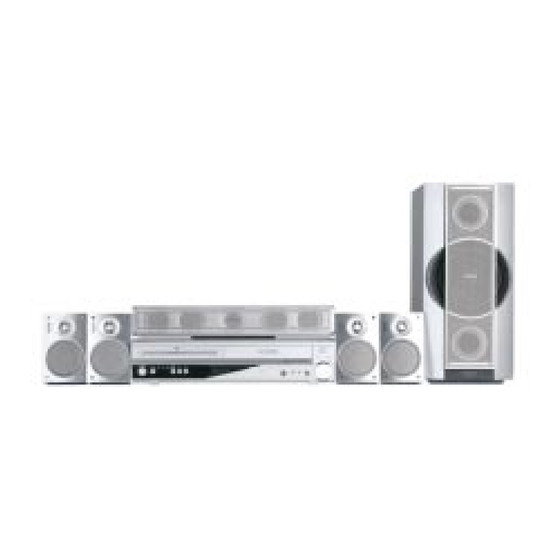
DVD-VCR Receiver
Service
Service
Service
Service
Service
Service Manual
CONTENTS
Section 1: Main Section
Adjustment Procedure
Schematic Diagrams and CBAs (PC Boards)
Exploded Views
Electrical & Mechanical Parts List
Section 2: VCR Deck Mechanism Section
Standard maintenance
Mechanical alignment Procedures
Disassembly / Assembly of Mechanism
Deck Exploded views
Mechanism Parts List
Section 3
Revision List
©
Copyright 2003 Philips Consumer Electronics B.V. Eindhoven, The Netherlands
All rights reserved. No part of this publication may be reproduced, stored in a retrieval system or
transmitted, in any form or by any means, electronic, mechanical, photocopying, or otherwise
without the prior permission of Philips.
Published by KC 0339 Service Audio
Version 1.0
CLASS 1
LASER PRODUCT
Printed in The Netherlands
Subject to modification
MX5100VR/
SURVEY OF VERSIONS:
/00
PAL I
/05
PAL B/G
/02
PAL B/G,L,L' & SECAM B/G,L,L'
00/02/05
GB
3139 785 30490
Advertisement
Chapters
Table of Contents

Subscribe to Our Youtube Channel
Related Manuals for Philips MX5100VR/00


Summary of Contents for Philips MX5100VR/00
- Page 1 Revision List © Copyright 2003 Philips Consumer Electronics B.V. Eindhoven, The Netherlands All rights reserved. No part of this publication may be reproduced, stored in a retrieval system or transmitted, in any form or by any means, electronic, mechanical, photocopying, or otherwise without the prior permission of Philips.
-
Page 2: Table Of Contents
MAIN SECTION DIGITAL VIDEO DISC PLAYER, VIDEO CASSETTE RECORDER & FM/MW RADIO TUNER Sec. 1: Main Section I Adjustment Procedures I Schematic Diagrams and CBA’s I Exploded Views I Mechanical and Electrical Parts List TABLE OF CONTENTS LASER BEAM SAFETY PRECAUTIONS ........... . . 1-1-1 IMPORTANT SAFETY PRECAUTIONS . -
Page 3: Laser Beam Safety Precautions
LASER BEAM SAFETY PRECAUTIONS This DVD player uses a pickup that emits a laser beam. Do not look directly at the laser beam coming from the pickup or allow it to strike against your skin. The laser beam is emitted from the location shown in the figure. When checking the laser diode, be sure to keep your eyes at least 30cm away from the pickup lens when the diode is turned on. -
Page 4: Important Safety Precautions
IMPORTANT SAFETY PRECAUTIONS Product Safety Notice I. Also check areas surrounding repaired locations. J. Use care that foreign objects (screws, solder drop- Some electrical and mechanical parts have special lets, etc.) do not remain inside the set. safety-related characteristics which are often not evi- K. -
Page 5: Safety Check After Servicing
Safety Check after Servicing Chassis or Secondary Conductor Examine the area surrounding the repaired location for damage or deterioration. Observe that screws, parts, and wires have been returned to their original posi- Primary Circuit Terminals tions. Afterwards, do the following tests and confirm the specified values to verify compliance with safety standards. -
Page 6: Standard Notes For Servicing
STANDARD NOTES FOR SERVICING Circuit Board Indications How to Remove / Install Flat Pack-IC a. The output pin of the 3 pin Regulator ICs is indi- 1. Removal cated as shown. With Hot-Air Flat Pack-IC Desoldering Machine:. (1) Prepare the hot-air flat pack-IC desoldering Top View Bottom View machine, then apply hot air to the Flat Pack-IC... - Page 7 With Soldering Iron: (4) Bottom of the flat pack-IC is fixed with glue to the CBA; when removing entire flat pack-IC, first apply (1) Using desoldering braid, remove the solder from all soldering iron to center of the flat pack-IC and heat pins of the flat pack-IC.
- Page 8 2. Installation Instructions for Handling Semi-conductors (1) Using desoldering braid, remove the solder from the foil of each pin of the flat pack-IC on the CBA so Electrostatic breakdown of the semi-conductors may you can install a replacement flat pack-IC more occur due to a potential difference caused by electro- easily.
-
Page 9: Preparation For Servicing
PREPARATION FOR SERVICING How to Enter the Service Mode About Optical Sensors Caution: An optical sensor system is used for the Tape Start and End Sensors on this equipment. Carefully read and follow the instructions below. Otherwise the unit may operate erratically. What to do for preparation Insert a tape into the Deck Mechanism Assembly and press the PLAY button. -
Page 10: Operating Controls And Functions
OPERATING CONTROLS AND FUNCTIONS [ MX5100VR/00 ] 1-5-1 E9015IB... - Page 11 1-5-2 E9015IB...
- Page 12 1-5-3 E9015IB...
- Page 13 [ MX5100VR/05 ] 1-5-4 E9016IB...
- Page 14 1-5-5 E9016IB...
- Page 15 1-5-6 E9016IB...
- Page 16 [ MX5100VR/02 ] 1-5-7 E9017IB...
- Page 17 1-5-8 E9017IB...
- Page 18 1-5-9 E9017IB...
-
Page 19: Signal Name Abbreviations
SIGNAL NAME ABBREVIATIONS Signal Name Function Signal Name Function A/D Converter Power Input/ AVcc Standard Voltage Input FIP Drive Power Supply 2 Channel Audio Signal C-CONT Capstan Motor Control Signal 33/36M DA Converter Clock Capstan Motor FWD/REV Control C-F/R Signal (FWD=”L”/REV=”H”) Dolby Digital 5.1ch Audio Signal Capstan Motor Rotation Detection C-FG... - Page 20 Signal Name Function Signal Name Function HDPH-DET Headphone Detecting Signal SCART 8Pin DVD Input Control DVD-8PIN-IN Signal Headphone Left/Right Output HDPH-L/R Signal DVD-AUDIO DVD Audio Control Signal Hi-Fi-A Hi-Fi Audio Head DVD Component Video Signal DVD-B-OUT (blue) Hi-Fi-COM Hi-Fi Audio Head Common DVD Component Video Signal DVD-G-OUT Hi-Fi-H-SW...
- Page 21 Signal Name Function Signal Name Function P-OFF-H Power Off at High Take Up Reel T-REEL Rotation Signal P-ON+15V +15V at Power-On Signal TIMER LED “TIMER” LED Signal Output P-ON+44V +44V at Power-On Signal TIMER+5V +5V at Timer P-ON+5V +5V at Power-On Signal TIMER- LED “TIMER”...
-
Page 22: Location Of Cbas (Pc Boards)
LOCATION OF CBAS (PC BOARDS) Power Supply (Audio Module) board DAC CBA Speaker Connector board Power Supply (For VCR/DVD) CBA Power Amplifier board AF board DVD Main CBA Unit AM/FM Tuner Unit Jack-B CBA Jack-A CBA LED CBA Jack C CBA DVD OPEN/CLOSE CBA Tuner CBA AFV CBA... -
Page 23: Cabinet Disassembly Instructions
CABINET DISASSEMBLY INSTRUCTIONS 1. Disassembly Flowchart REMOVAL REMOVE/*UNHOOK/ LOC. PART This flowchart indicates the disassembly steps to gain Fig. UNLOCK/RELEASE/ Note access to item(s) to be serviced. When reassembling, UNPLUG/DESOLDER follow the steps in reverse order. Bend, route, and dress the cables as they were originally. DVD Main D5 *CN201, *CN301 CBA Unit... - Page 24 Note: [1] Top Cover (1): Identification (location) No. of parts in the figures (S-1) (2): Name of the part (S-1) (3): Figure Number for reference (4): Identification of parts to be removed, unhooked, unlocked, released, unplugged, unclamped, or desoldered. P=Spring, L=Locking Tab, S=Screw, CN=Connector *=Unhook, Unlock, Release, Unplug, or Desolder e.g.
- Page 25 (S-7) (S-8) (S-8) (S-8) CN1008 CN902 Earth Plate CN601 (S-6) (S-9) [8] PS CBA Holder (S-6) CN901 [9] Power Supply CBA (S-9) [5] DVD Mecha Unit (For VCR/DVD) (S-9) (S-6) CN050 CN401 Fig. D6 (S-13) (S-14) [12] Fan Cover (S-13) (S-14) [11] Fan (S-13)
- Page 26 (S-20) FE Head Cylinder Assembly [17] Deck Assembly SW507 LD-SW Cylinder Shield Main CBA [17] Deck Assembly AC Head Assembly Cam Gear Main CBA Hole Shaft Hole LD-SW Main CBA (S-21) (S-22) From Lead with From Cylinder blue stripe FE Head Assembly From AC Head...
- Page 27 Pedestal Shield [20] Jack-B [19] DAC CBA (S-25) (S-25) Desolder (S-25) [21] Jack-A Lead with CN7105 blue stripe (S-25) [22] Main CN7104 [25] Side Bracket [24] Deck Pedestal (S-26) [18] DVD OPEN/ CN2018 CLOSE CBA CN2017 Fig. D10 Fig. D12 (S-22) Trans Holder Trans...
- Page 28 HOW TO MANUAL EJECT 1. Remove the Top Case. 2. Rotate this roulette in the direction of the arrow as shown below. Top Cover Mecha Rotate this roulette in Deck Assembly the direction of the arrow Tray 1-8-6 E9015DC...
-
Page 29: Electrical Adjustment Instructions
ELECTRICAL ADJUSTMENT INSTRUCTIONS General Note: "CBA" is an abbreviation for "Circuit Board Assembly." NOTE: Figure 1 1.Electrical adjustments are required after replacing circuit components and certain mechanical parts. It is important to do these adjustments only after all EXT. Syncronize Trigger Point repairs and replacements have been completed. -
Page 30: Firmware Renewal Mode
FIRMWARE RENEWAL MODE 1. Turn the power on and remove the disc on the tray. 5. After programming is finished, the tray opens auto- 2. To put the DVD player into version up mode, press matically. Fig. e appears on the screen and the [9], [8], [7], [6], and [SEARCH MODE] buttons on checksum in (*3) of Fig. -
Page 31: Block Diagrams
" = SMD 1. PREFIX SYMBOL "CN" MEANS CONNECTOR. :INDICATES A TEST POINT WITH A JUMPER WIRE ACROSS A HOLE IN THE PCB. MX5100VR/00 (CAN DISCONNECT AND RECONNECT.) :USED TO INDICATE A TEST POINT WITH A COMPONENT LEAD ON FOIL SIDE. - Page 32 Model Mark HOLES OF THE PCB. :USED TO INDICATE A TEST POINT WITH A TEST PIN. REC-VIDEO SIGNAL PB-VIDEO SIGNAL DVD VIDEO SIGNAL (WIRE IS SOLDERED DIRECTLY.) MX5100VR/00 IC631 (VPS) MX5100VR/05 MAIN CBA DAVN-L DAVN-L MX5100VR/02 IIC-BUS SDA TO SERVO/SYSTEM...
- Page 33 Audio Block Diagram PB-AUDIO SIGNAL REC-AUDIO SIGNAL DVD AUDIO SIGNAL Mode : SP/REC MAIN CBA N-A-PB TO Hi-Fi N-A-REC AUDIO BLOCK IC301 (AUDIO SIGNAL PROCESS) TUNER PB-ON LINE MUTE (DECK ASSEMBLY) SP/LP-ON ACE HEAD ASSEMBLY REC-ON Q404 CL287 CL504 AUDIO A-PB/REC 4 4 A-PB/REC Q403...
- Page 34 :USED TO INDICATE A TEST POINT WITH NO TEST PIN. (CAN DISCONNECT AND RECONNECT.) :USED TO INDICATE A TEST POINT WITH A TEST PIN. 2. PREFIX SYMBOL "CL" MEANS WIRE-SOLDER MX5100VR/00 HOLES OF THE PCB. MX5100VR/05 (WIRE IS SOLDERED DIRECTLY.)
- Page 35 Audio Amp Block Diagram NOTE FOR WIRE CONNECTORS: PB-AUDIO SIGNAL REC-AUDIO SIGNAL DATA(AUDIO) SIGNAL DVD AUDIO SIGNAL 1. PREFIX SYMBOL "CN" MEANS CONNECTOR. (CAN DISCONNECT AND RECONNECT.) AMP UNIT 2. PREFIX SYMBOL "CL" MEANS WIRE-SOLDER " " = SMD HOLES OF THE PCB. (WIRE IS SOLDERED DIRECTLY.) CN2020 HDPH-R...
- Page 36 Power Supply ( For VCR/DVD ) Block Diagram NOTE : CAUTION CAUTION ! FOR CONTINUED PROTECTION AGAINST FIRE HAZARD, Fixed voltage (or Auto voltage selectable ) power supply circuit is used in this unit. The voltage for parts in hot circuit is measured using If Main Fuse (F1001) is blown, check to see that all components in the power supply REPLACE ONLY WITH THE SAME TYPE T1.6A L 250V FUSE.
- Page 37 DVD System Control/Servo Block Diagram NOTE FOR WIRE CONNECTORS: " " = SMD 1. PREFIX SYMBOL "CN" MEANS CONNECTOR. (CAN DISCONNECT AND RECONNECT.) 2. PREFIX SYMBOL "CL" MEANS WIRE-SOLDER FOCUS SERVO SIGNAL TRACKING SERVO SIGNAL SLED SERVO SIGNAL SPINDLE SERVO SIGNAL HOLES OF THE PCB.
- Page 38 Digital Signal Process Block Diagram DATA(AUDIO) SIGNAL DATA(VIDEO/AUDIO) SIGNAL DVD VIDEO SIGNAL IC102 (SDRAM) IC101 (MICRO CONTROLLER) SDRAM ADDRESS(0-10) SDRAM ADDRESS(0-10) DATA SDRAM EXTERNAL MEMORY DECODER INST. DECODER STREAM SDRAM DATA(0-31) SDRAM DATA(0-31) DATA PIXEL OPERATION INST. DATA CN201 SIGNAL DVD/CD PROCESSOR PCM-DATA0...
- Page 39 DVD Video Block Diagram NOTE FOR WIRE CONNECTORS: " " = SMD 1. PREFIX SYMBOL "CN" MEANS CONNECTOR. (CAN DISCONNECT AND RECONNECT.) 2. PREFIX SYMBOL "CL" MEANS WIRE-SOLDER HOLES OF THE PCB. (WIRE IS SOLDERED DIRECTLY.) DVD VIDEO SIGNAL DVD MAIN CBA UNIT MAIN CBA TO VIDEO DVD-VIDEO...
- Page 40 DVD Audio Block Diagram NOTE FOR WIRE CONNECTORS: 1. PREFIX SYMBOL "CN" MEANS CONNECTOR. (CAN DISCONNECT AND RECONNECT.) 2. PREFIX SYMBOL "CL" MEANS WIRE-SOLDER " " = SMD HOLES OF THE PCB. (WIRE IS SOLDERED DIRECTLY.) DATA(AUDIO) SIGNAL DVD AUDIO SIGNAL DVD MAIN CBA UNIT CN901 CN7102...
-
Page 41: Schematic Diagrams / Cba's And Test Points
SCHEMATIC DIAGRAMS / CBA'S AND TEST POINTS Standard Notes Notes: WARNING 1. Do not use the part number shown on these draw- ings for ordering. The correct part number is Many electrical and mechanical parts in this chassis shown in the parts list, and may be slightly different have special characteristics. - Page 42 Main 1/11 Schematic Diagram Parts Location Guide Ref No. Position Ref No. Position Ref No. Position RESISTORS CAPACITORS CAPACITORS C505 C556 R545 C506 R546 CONNECTORS C508 CL501 R547 C509 CL502 R548 C510 CL504 R552 DIODES C511 R554 C513 D510 R555 C514 D511 R558...
- Page 43 0.00 ~ 0.51V REC/OTR -------------- MODEL MARK 0.51 ~ 0.92V POWER -------------- <5.0> THE SAME VOLTAGE FOR BOTH MX5100VR/00 0.92 ~ 1.27V OUTPUT PLAY INDICATES THAT THE VOLTAGE PLAY, REC & DVD MODES. MX5100VR/05 1.27 ~ 1.61V STOP/EJECT -------------- IS NOT CONSISTENT HERE.
- Page 44 Main 2/11 & Sensor Schematic Diagram < VCR Section > FL2001 MATRIX CHART “ “ = SMD PLAY MODE Note: REC MODE When replacing one of the following parts, (2.5) DVD MODE REPEAT <5.0> all of them should be replaced: D501, D504. THE SAME VOLTAGE FOR BOTH INDICATES THAT THE VOLTAGE PLAY, REC &...
- Page 45 Main 2/11 Schematic Diagram Parts Location Guide Ref No. Position Ref No. Position CAPACITORS RESISTORS C502 R522 C611 R523 C614 R525 C615 R526 R528 CONNECTORS CN503 R529 CN505 R530 DIODES R531 D501 R532 D504 R533 R534 IC611 R535 IC612 R549 TRANSISTORS R550 Q502...
- Page 46 Main 3/11 Schematic Diagram Parts Location Guide Ref No. Position Ref No. Position Ref No. Position Ref No. Position TRANSISTORS RESISTORS CAPACITORS CAPACITORS C251 C347 Q302 R402 C252 C348 Q401 R404 C253 C349 Q403 R405 C254 C350 Q404 R406 C301 C402 Q405 R407...
- Page 47 Comparison Chart of “ “ = SMD REC MODE Models and Marks (2.5) DVD MODE <5.0> THE SAME VOLTAGE FOR BOTH MODEL MARK INDICATES THAT THE VOLTAGE PLAY, REC & DVD MODES. MX5100VR/00 IS NOT CONSISTENT HERE. MX5100VR/05 MX5100VR/02 1-12-9 1-12-10 E9015SCM3...
- Page 48 Main 4/11 Schematic Diagram < VCR Section > “ “ = SMD PLAY MODE REC MODE (2.5) DVD MODE <5.0> THE SAME VOLTAGE FOR BOTH INDICATES THAT THE VOLTAGE PLAY, REC & DVD MODES. IS NOT CONSISTENT HERE. 1-12-11 1-12-12 E9015SCM4...
- Page 49 Main 4/11 Schematic Diagram Parts Location Guide Ref No. Position Ref No. Position TRANSISTORS CAPACITORS C451 Q451 C452 RESISTORS C453 R451 C454 R452 C455 R453 C456 R454 C457 R455 C458 R456 C461 R457 C462 R458 C463 R459 C464 R460 C465 R461 C466 R462...
- Page 50 Main 5/11 Schematic Diagram Parts Location Guide Ref No. Position Ref No. Position TRANSISTORS CAPACITORS C1201 Q1202 C1202 Q1203 C1205 Q1204 C1206 Q1352 C1207 Q1502 AA-4 C1208 RESISTORS C1221 R1203 C1222 R1204 C1223 AA-1 R1205 C1224 AA-1 R1206 C1245 R1207 C1246 R1208 C1247...
- Page 51 Main 5/11 Schematic Diagram < VCR Section> PLAY MODE “ “ = SMD REC MODE (2.5) DVD MODE <5.0> THE SAME VOLTAGE FOR BOTH INDICATES THAT THE VOLTAGE PLAY, REC & DVD MODES. IS NOT CONSISTENT HERE. 1-12-15 1-12-16 E9015SCM5...
- Page 52 Main 6/11 Schematic Diagram < VCR Section > “ “ = SMD PLAY MODE REC MODE (2.5) DVD MODE <5.0> THE SAME VOLTAGE FOR BOTH INDICATES THAT THE VOLTAGE PLAY, REC & DVD MODES. IS NOT CONSISTENT HERE. MAIN 6/11 Schematic Diagram Parts Location Guide Ref No.
- Page 53 Models and Marks (2.5) DVD MODE <5.0> THE SAME VOLTAGE FOR BOTH MODEL MARK INDICATES THAT THE VOLTAGE PLAY, REC & DVD MODES. MX5100VR/00 IS NOT CONSISTENT HERE. MX5100VR/05 MX5100VR/02 MAIN 7/11 Schematic Diagram Parts Location Guide Ref No. Position CAPACITORS...
- Page 54 Main 8/11 & DVD OPEN/CLOSE Schematic Diagram < VCR Section> PLAY MODE “ “ = SMD REC MODE (2.5) DVD MODE <5.0> THE SAME VOLTAGE FOR BOTH INDICATES THAT THE VOLTAGE PLAY, REC & DVD MODES. IS NOT CONSISTENT HERE. 1-12-21 1-12-22 E9015SCM8...
- Page 55 Main 8/11 Schematic Diagram Parts Location Guide Ref No. Position Ref No. Position CAPACITORS RESISTORS C2004 AQ-1 R653 AM-2 C2008 AO-3 R654 AM-1 C2009 AO-3 R655 AM-1 C2012 AQ-1 R2005 AQ-1 C2013 AN-1 R2022 AN-3 C2014 AN-1 R2027 AO-3 C2015 AN-1 R2038 AO-4...
- Page 56 Main 9/11 Schematic Diagram Parts Location Guide Ref No. Position Ref No. Position Ref No. Position COILS RESISTORS CAPACITORS C056 AU-4 L1052 AT-2 R061 AV-4 C057 AU-3 L2006 AT-2 R062 AU-3 TRANSISTORS C058 AU-3 R064 AU-2 C059 AU-3 Q051 AT-4 R065 AU-3 C060...
- Page 57 Main 9/11 Schematic Diagram < VCR Section > “ “ = SMD PLAY MODE REC MODE (2.5) DVD MODE <5.0> THE SAME VOLTAGE FOR BOTH INDICATES THAT THE VOLTAGE PLAY, REC & DVD MODES. IS NOT CONSISTENT HERE. 1-12-25 1-12-26 E9015SCM9...
- Page 58 Main 10/11 Schematic Diagram < VCR Section> “ “ = SMD PLAY MODE REC MODE (2.5) DVD MODE <5.0> THE SAME VOLTAGE FOR BOTH INDICATES THAT THE VOLTAGE PLAY, REC & DVD MODES. IS NOT CONSISTENT HERE. MAIN 10/11 Schematic Diagram Parts Location Guide Ref No.
- Page 59 Main 11/11 Schematic Diagram < VCR Section > “ “ = SMD PLAY MODE REC MODE (2.5) DVD MODE <5.0> THE SAME VOLTAGE FOR BOTH INDICATES THAT THE VOLTAGE PLAY, REC & DVD MODES. IS NOT CONSISTENT HERE. MAIN 11/11 Schematic Diagram Parts Location Guide Ref No.
- Page 60 Main CBA Parts Location Guide Ref No. Position Ref No. Position Ref No. Position Ref No. Position Ref No. Position Ref No. Position Ref No. Position Ref No. Position Ref No. Position Ref No. Position Ref No. Position Ref No. Position CAPACITORS CAPACITORS...
- Page 61 Main CBA Top View Sensor CBA Top View BHB300F01014-A BHB300F01014-B TP751 V-OUT TP301 C-PB VR501 SW-P TP503 TP501 S-INH TP504 RF-SW 1-12-33 1-12-34 BE9015F01011A...
- Page 62 Main CBA Bottom View 1-12-35 1-12-36 BE9015F01011A...
- Page 63 PLAY MODE REC MODE (2.5) DVD MODE <5.0> THE SAME VOLTAGE FOR BOTH INDICATES THAT THE VOLTAGE PLAY, REC & DVD MODES. IS NOT CONSISTENT HERE. Comparison Chart of Models and Marks MODEL MARK MX5100VR/00 MX5100VR/05 MX5100VR/02 1-12-37 1-12-38 E9015SCP...
- Page 64 Power Supply (For VCR/DVD) Schematic Diagram Parts Location Guide Power Supply (For VCR/DVD) CBA Parts Location Guide POWER SUPPLY Schematic Diagram Parts Location Guide POWER SUPPLY CBA Parts Location Guide Ref No. Position Ref No. Position Ref No. Position Ref No. Position Ref No.
- Page 65 Power Supply (For VCR/DVD) CBA Top View Power Supply (For VCR/DVD) CBA Bottom View CAUTION ! CAUTION ! BECAUSE A HOT CHASSIS GROUND IS PRESENT IN THE POWER For continued protection against fire hazard, Fixed voltage ( or Auto voltage selectable ) power supply circuit is used in this unit. SUPPLY CIRCUIT , AN ISOLATION TRANSFORMER MUST BE USED.
- Page 66 Models and Marks (2.5) DVD MODE <5.0> THE SAME VOLTAGE FOR BOTH MODEL MARK INDICATES THAT THE VOLTAGE PLAY, REC & DVD MODES. MX5100VR/00 IS NOT CONSISTENT HERE. MX5100VR/05 MX5100VR/02 TUNER Schematic Diagram Parts Location Guide Ref No. Position CAPACITORS...
- Page 67 Tuner CBA Top View TUNER CBA Parts Location Guide Ref No. Position CAPACITORS C701 C703 C706 C708 C709 C711 C712 C714 C715 C716 CONNECTORS CN701 CN703 CN1201 CN2013 CN2014 DIODE D701 COILS L701 L702 L703 L704 Tuner CBA Bottom View RESISTORS R703 R704...
- Page 68 DAC Schematic Diagram < VCR Section > PLAY MODE “ “ = SMD REC MODE (2.5) DVD MODE <5.0> THE SAME VOLTAGE FOR BOTH INDICATES THAT THE VOLTAGE PLAY, REC & DVD MODES. IS NOT CONSISTENT HERE. 1-12-47 1-12-48 E9015SCAV...
- Page 69 DAC Schematic Diagram Parts Location Guide Ref No. Position Ref No. Position Ref No. Position Ref No. Position Ref No. Position Ref No. Position Ref No. Position CAPACITORS CAPACITORS CAPACITORS TRANSISTORS RESISTORS RESISTORS RESISTORS C7103 C7341 C7543 Q7308 R7207 R7402 R7508 C7105 C7342...
- Page 70 DAC CBA Top View DAC CBA Bottom View BE9015F02011 1-12-51 1-12-52...
- Page 71 DAC CBA Parts Location Guide Ref No. Position Ref No. Position Ref No. Position Ref No. Position Ref No. Position Ref No. Position Ref No. Position CAPACITORS CAPACITORS CAPACITORS TRANSISTORS RESISTORS RESISTORS RESISTORS C7103 C7341 C7543 Q7308 R7207 R7402 R7508 C7105 C7342 C7544...
- Page 72 Front Schematic Diagram < VCR Section > Note: When replacing one of the following parts, all of them should be replaced: D2011, D2012, D2013, D2014, D2015. PLAY MODE “ “ = SMD REC MODE (2.5) DVD MODE <5.0> THE SAME VOLTAGE FOR BOTH INDICATES THAT THE VOLTAGE PLAY, REC &...
- Page 73 Front CBA Top View Front CBA Bottom View FRONT CBA Parts Location Guide Ref No. Position CONNECTOR CL508 CN2015 DIODES D2011 D2012 D2013 D2014 D2015 RESISTORS R2071 R2072 R2073 R2074 R2075 SWITCH SW502 VARIABLE RESISTOR VR502 BE9015F01031B DVD OPEN/CLOSE CBA Top View DVD OPEN /CLOSE CBA Bottom View BE9015F01011B 1-12-57...
- Page 74 LED Schematic Diagram <VCR Section> PLAY MODE “ “ = SMD REC MODE Note: (2.5) DVD MODE When replacing one of the following parts, <5.0> THE SAME VOLTAGE FOR BOTH all of them should be replaced: D651, D652, D653, D654. INDICATES THAT THE VOLTAGE PLAY, REC &...
- Page 75 (2.5) DVD MODE <5.0> THE SAME VOLTAGE FOR BOTH MODEL MARK INDICATES THAT THE VOLTAGE PLAY, REC & DVD MODES. IS NOT CONSISTENT HERE. MX5100VR/00 MX5100VR/05 MX5100VR/02 JACK-A Schematic Diagram Parts Location Guide Ref No. Position Ref No. Position CAPACITORS...
- Page 76 Jack-A CBA Top View Jack-A CBA Bottom View JACK-A CBA Parts Location Guide Ref No. Position Ref No. Position CAPACITORS TRANSISTORS C104 Q111 C107 Q112 C109 Q113 C112 Q114 RESISTORS C113 C114 R112 C116 R113 C117 R116 C118 R119 C127 R124 CONNECTOR R128...
- Page 77 JACK-B & Junction-B Schematic Diagram < VCR Section > PLAY MODE “ “ = SMD REC MODE (2.5) DVD MODE <5.0> THE SAME VOLTAGE FOR BOTH INDICATES THAT THE VOLTAGE PLAY, REC & DVD MODES. IS NOT CONSISTENT HERE. JACK-B Schematic Diagram Parts Location Guide Ref No.
- Page 78 Jack-B CBA Top View Jack-B CBA Bottom View JACK-B CBA Parts Location Guide Ref No. Position CAPACITORS C101 C102 C105 C106 C108 C110 C111 C119 CONNECTOR CL2117 DIODES D101 D102 D105 D107 D112 D113 COIL L102 TRANSISTOR BE9015F01031C Q103 RESISTORS R111 R114 R117...
- Page 79 JACK-C Schematic Diagram < VCR Section > JACK-C Schematic Diagram Parts Location Guide Ref No. Position CAPACITORS C1353 C1354 C1355 C1359 CONNECTOR CN1202 COILS L1251 L1351 TRANSISTOR Q1351 RESISTORS R1352 R1353 R1354 R1355 R1356 R1361 MISCELLANEOUS JK1202 JACK-C CBA E9015SCJC Parts Location Guide Ref No.
- Page 80 Models and Marks PLAY MODE “ “ = SMD REC MODE MODEL MARK (2.5) DVD MODE MX5100VR/00 <5.0> THE SAME VOLTAGE FOR BOTH MX5100VR/05 INDICATES THAT THE VOLTAGE PLAY, REC & DVD MODES. IS NOT CONSISTENT HERE. AFV Schematic Diagram MX5100VR/02 Parts Location Guide Ref No.
- Page 81 AFV CBA Top View AFV CBA Bottom View AFV CBA Parts Location Guide Ref No. Position CAPACITORS CONNECTOR DIODE BHC400F01091 COILS RESISTORS MISCELLANEOUS 1-12-73 1-12-74...
- Page 82 DVD Main 1/3 Schematic Diagram < DVD Section > PLAY MODE “ “ = SMD STOP MODE (2.5) THE SAME VOLTAGE FOR INDICATES THAT THE VOLTAGE BOTH PLAY & STOP MODES. IS NOT CONSISTENT HERE. 1-12-75 1-12-76 E9015SCD1...
- Page 83 DVD Main 2/3 Schematic Diagram < DVD Section > PLAY MODE “ “ = SMD STOP MODE (2.5) THE SAME VOLTAGE FOR INDICATES THAT THE VOLTAGE BOTH PLAY & STOP MODES. IS NOT CONSISTENT HERE. 1-12-77 1-12-78 E9015SCD2...
- Page 84 IC101 VOLTAGE CHART PIN.NO PLAY STOP PIN.NO PLAY STOP PIN.NO PLAY STOP PIN.NO PLAY STOP PIN.NO PLAY STOP PIN.NO PLAY STOP PIN.NO PLAY STOP PIN.NO PLAY STOP ----- ----- ----- ----- ----- ----- ----- ----- ----- ----- ----- ----- ----- ----- ----- -----...
- Page 85 DVD Main 3/3 Schematic Diagram < DVD Section > PLAY MODE “ “ = SMD STOP MODE (2.5) THE SAME VOLTAGE FOR INDICATES THAT THE VOLTAGE BOTH PLAY & STOP MODES. IS NOT CONSISTENT HERE. 1-12-81 1-12-82 E9015SCD3...
- Page 86 AM/FM Tuner Unit Schematic Diagram < AMP UNIT Section > 1101 A2 5121 E11 1102 B1 5122 H5 1103 E2 5123 G5 1110 B2 6105-1 E4 VERSION PROGRAMMING COMPONENTS 1120 E14 6105-2 G6 TUNER BOARD ECO6 1130 A2 6106 D4 / SYSTEMS-CENELEC 1131 C2 6107 G13...
- Page 87 AM/FM Tuner Unit Top & Bottom View 1101 B5 1110 B4 1131 C5 2107 B3 2133 C1 2162 A4 5102 C4 5110 A2 5114 A2 5121 B2 7104 C4 9101 A2 9104 B1 9107 B4 9110 A4 TUNER ADJUSTMENT TABLE ( ECO6 Cenelec FM/MW - and FM/MW/LW - versions with AM-frame aerial ) 1102 B5 1120 A4...
- Page 88 AF 1/4 Schematic Diagram < AMP UNIT Section > U4 B7 T136 F13 U6 B6 U101 B6 1100 A6 U102 B7 1101 A7 U103 B7 1237 D1 2100 A3 2101 A3 2102 C4 T130 2101 3100 2103 E3 6CH_L 2104 E3 2110 C9 T117 VREF...
- Page 89 AF 2/4 Schematic Diagram < AMP UNIT Section > 1232 H13 1233 H11 1234 F11 1235 F13 2200 E2 2201 E1 3204 3205 2202 D2 2203 E2 2204 E3 2205 E4 2206 F9 7231 2230 B8 7232 BC857B 5.4V 2232 D10 3206 BC847B 7200...
- Page 90 AF 3/4 Schematic Diagram < AMP UNIT Section > 1231 C13 T340 D13 1238 E13 T342 D13 2300 C2 2301 A6 2302 A9 2303 A8 2304 G2 2305 E6 3302 GND_S 2306 E8 3351 2307 E9 2310 D4 2311 D4 7330 4.7V 4.7V...
- Page 91 AF 4/4 Schematic Diagram < AMP UNIT Section > 1236 A8 T516 A7 1239 A7 T517 A7 2530 H1 T518 A7 2531 H1 T519 A8 FE-BT-VK-N FE-BT-VK-N 2532 I1 T520 A8 2533 I1 T521 A8 2560 G5 T523 A9 2562 I5 T524 A9 2563 H6 T526 A9...
- Page 92 AF BOARD Top View AV_OSAKA / 3139 113 3517 pt 5 dd wk 335 1-12-95 1-12-96 31391133517pt5...
- Page 93 AF BOARD Bottom View AV_OSAKA / 3139 113 3517 pt 5 dd wk 335 1-12-97 1-12-98 31391133517pt5...
- Page 94 Power Amplifier 1/2 Schematic Diagram < AMP UNIT Section > 1301 B1 7716 I12 1302 B2 F100 B3 1303 E2 F102 B3 1304 G2 F103 B3 1305 E1 F105 B3 1309 G1 F106 C3 1312 G3 F108 C3 1320 I6 F111 C3 1400 I6 F114 C3...
- Page 95 Power Amplifier 2/2 Schematic Diagram < AMP UNIT Section > 1306 A7 5303 I5 1307 H7 7100 A2 1308 E7 7200 D2 1316 B7 7300 H2 2106 1317 I7 1318 E7 2104 2107 2101 A3 2102 A3 100n 100n 2104 A4 2101 2102 2105...
- Page 96 Power Amplifier BOARD Top View This assemby drawing shows a summary of all possible versions. For components used in a specific version see schematic and respective parts list. PART C PART D 3104 213 3525p5 dd wk0334 31042133525p5 1-12-103 1-12-104...
- Page 97 Power Amplifier BOARD Bottom View This assemby drawing shows a summary of all possible versions. For components used in a specific version see schematic and respective parts list. PART A PART B 3104 213 3525p5 dd wk0334 1-12-105 1-12-106 31042133525p5...
- Page 98 Power Supply (AUDIO MODULE) Schematic Diagram < AMP UNIT Section > CAUTION FOR CONTINUED PROTECTION AGAINST FIRE HAZARD, REPLACE ONLY WITH THE SAME TYPE FUSE. 1200,1203: T5A 250V, 1204,1205: T4A 250V Mfr: WICKMANN-WERKE GMBH TYPE NO.: 372. ATTENTION AFIN D’ASSURER UNE PROTECTION CONTINUE CONTRE LES RISQUES D’INCENDIE, UTILISER UNIQUEMENT UN FUSIBLE DU MEME TYPE POUR LE REMPLACEMENT.
- Page 99 Power Supply (AUDIO MODULE) BOARD Top & Bottom View CAUTION FOR CONTINUED PROTECTION AGAINST FIRE HAZARD, REPLACE ONLY WITH THE SAME TYPE FUSE. 1200,1203: T5A 250V, 1204,1205: T4A 250V Mfr: WICKMANN-WERKE GMBH TYPE NO.: 372. ATTENTION AFIN D’ASSURER UNE PROTECTION CONTINUE CONTRE LES RISQUES D’INCENDIE, UTILISER UNIQUEMENT UN FUSIBLE DU MEME TYPE POUR LE REMPLACEMENT.
- Page 100 Speaker Connector Schematic Diagram < AMP UNIT Section > 1303-A E4 1303-B B4 1303-C A4 1303-D D4 1303-E C4 To Amp 1303-F B4 1304-A B3 1304-B A3 1304-B 1303-C EH-B 1313 2012 3000 2000 1304-C D3 1304-D C3 220n 1304-E B3 2001 1313 A1 LQR1910...
- Page 101 Speaker Connector BOARD Top & Bottom View This assemby drawing shows a summary of all possible versions. For components used This assemby drawing shows a summary of all possible versions. For components used in a specific version see schematic and respective parts list. in a specific version see schematic and respective parts list.
-
Page 102: Waveforms
WAVEFORMS (TP301 of Main CBA) UPPER (TP504 of Main CBA) LOWER C-PB 10mV x 10 RF-SW 0.5V x 10 5msec (TP751 of Main CBA) UPPER (TP504 of Main CBA) LOWER V-OUT 0.1V x 10 RF-SW 0.5V x 10 50usec (TP751 of Main CBA) V-OUT E-E 10usec 50mV x 10... - Page 103 WAVEFORMS NOTE: Input CD: 1kHz PLAY (WF7~WF9) DVD: POWER ON (STOP) MODE (WF4~WF6) Pin 1 of CN1601 Pin 13 of CN1601 AUDIO-L 0.5msec VIDEO-Y 0.2V 20µsec Pin 9 of CN1601 Pin 15 of CN1601 VIDEO-C 0.2V 20µsec AUDIO-R Pin 31 of IC1402 Pin 18 of CN1601 VIDEO-CVBS 0.5V...
-
Page 104: Wiring Diagram
WIRING DIAGRAM < VCR SECTION > NOTE FOR WIRE CONNECTORS: 1. PREFIX SYMBOL "CN" MEANS CONNECTOR. (CAN DISCONNECT AND RECONNECT.) 2. PREFIX SYMBOL "CL" MEANS WIRE-SOLDER HOLES OF THE PCB. (WIRE IS SOLDERED DIRECTLY.) FRONT HEADPHONE VIDEO IN AUDIO IN (R) AUDIO IN (L) (DECK ASSEMBLY) MAIN CBA CN2001... - Page 105 WIRING DIAGRAM < DVD SECTION > NOTE FOR WIRE CONNECTORS: 1. PREFIX SYMBOL "CN" MEANS CONNECTOR. (CAN DISCONNECT AND RECONNECT.) 2. PREFIX SYMBOL "CL" MEANS WIRE-SOLDER DVD MECHA HOLES OF THE PCB. (WIRE IS SOLDERED DIRECTLY.) DVD MAIN CBA UNIT SENSOR CN401 EV+1.5V...
-
Page 106: System Control Timing Charts
SYSTEM CONTROL TIMING CHARTS [ VCR Section ] Mode SW : LD-SW LD-SW Position detection A/D Input voltage Limit Symbol (Calculated voltage) 3.76V~4.50V (4.12V) 4.51V~5.00V (5.00V) 0.00V~0.25V (0.00V) 1.06V~1.50V (1.21V) 0.66V~1.05V (0.91V) 1.99V~2.60V (2.17V) 1.51V~1.98V (1.80V) 3.20V~3.75V (3.40V) 0.26V~0.65V (0.44V) 4.51V~5.00V (5.00V) 2.61V~3.19V... - Page 107 Still/Slow Control Frame Advance Timing Chart 1) SP Mode 18 RF-SW The first rise of RF-SW after a rise in F-AD signal F-AD (Internal Signal) "H" "H" "Z" C-DRIVE "L" "L" Stop detection (T2) Acceleration Detection (T1) Slow Tracking Value PB CTL Reversal Limit Value 20ms...
- Page 108 2) LP/SLP Mode 18 RF-SW The first rise of RF-SW after a rise in F-AD signal F-AD (Internal Signal) "H" "H" "Z" C-DRIVE "L" "L" Stop detection (T2) Acceleration Detection (T1) Slow Tracking Value PB CTL Reversal Limit Value 20ms 78 C-F/R 16 H-A-SW 15 ROTA...
- Page 109 EJECT ST-S/ END-S "OFF" CASS.LOAD LD-FWD 0.2s LD-REV 0.7s LD-FWD 0.4s LD-FWD 0.5s LD-REV STOP(A) PLAY LD-FWD PLAY LD-FWD LD-REV 0.2s LD-FWD PLAY PLAY PAUSE (SLOW) LD-FWD STILL(SLOW) PLAY LD-REV 0.2s LD-FWD PLAY STOP /EJECT LD-REV STOP(A) Fig. 3 1-15-4 E9015TI...
- Page 110 STOP(A) STOP LD-REV 0.2s LD-FWD STOP /EJECT LD-FWD 2.5s LD-FWD 0.5s LD-REV STOP(A) LD-REV 0.2s LD-FWD STOP /EJECT LD-FWD 2.5s LD-FWD 0.5s LD-REV STOP(A) LD-FWD PAUSE LD-FWD 2.5s Short REV LD-REV 0.2s LD-FWD REC PAUSE REC or PAUSE STOP /EJECT LD-FWD 1.0s LD-REV...
-
Page 111: Dvd Section
[ DVD Section ] Tray Close ~ Play / Play ~ Tray Open Disc Tray Tray Disc Stop Open Close Rotation Play 3.3V Tray OUT (TL220) 3.3V Tray IN (TL221) 1.65V Sled Drive (TP303) 1.65V Disc Drive (TP301) 1.65V Focus Drive (TP304) 1.65V Tracking Drive... -
Page 112: Ic Pin Function Descriptions
Comparison Chart of Models and Marks Signal Active Mark Function Name Level Model Mark Video Head Amp OUT H-A-SW MX5100VR/00 Switching Pulse MX5100VR/05 IN H-A- Head Amp COMP Comparator Signal MX5100VR/02 Video Head OUT RF-SW [ VCR Section ] Switching Pulse... - Page 113 Signal Active Signal Active Mark Function Mark Function Name Level Name Level IN Xin Main Clock Input Receiver Main TUNER- Power Supply OUT Xout Main Clock Input POWER Control Signal (OFF=“L”, ON=“H”) Vss(GND) DISPLAY- DVD FIP ON/OFF OUT INPUT ON/OFF Signal Input Select SELECT...
- Page 114 [ DVD Section ] Signal Active Mark Function Name Level IC612 [ PT6315 ] OUT A-MUTE- Audio Mute Control Signal (Mute = “H”) Signal In/Out Name Function Name CTL Frequency Characteristics Not Used OUT FF/REW-L Switching Signal (FF/REW=”L”) Not Used Tuner (AMP) VFD Not Used IN DISPLAY-...
- Page 115 Signal In/Out Name Function Name Not Used OUT 1G Grid Output OUT 2G Grid Output OUT 3G Grid Output OUT 4G Grid Output OUT 5G Grid Output OUT 6G Grid Output OUT 7G Grid Output OUT 8G Grid Output OUT 9G Grid Output Power Supply 1-16-4...
-
Page 116: Lead Identifications
LEAD IDENTIFICATIONS 2SA1175(J,H,F) 2SC1815-BL(TPE2) 2SK3566 MID-32A22 KTA1267(GR,Y) 2SC1815-Y(TPE2) MID-32A22F BA1F4M-T 2SC1815-GR(TPE2) PT204-6B-12 BN1F4M-T 2SC2120-Y(TPE2) KTC3203(Y) BN1L4M-T 2SA1015-GR(TPE2) KTA1266(GR) KTC3199(Y,GR,BL) KTC3198(Y,GR) 2SC2785(J,H,F,K) KTA1266(GR) KRC103M 2SA1020(Y) KRA103M 2SC3266-Y(TPE2) G D S KRA104M KTA1281(Y) KRA109M KTC3205(Y) PT6315 E C B E C B MSP3417G-QG-B8 MSP3417G-QG-B8-V3 NJM4558D... - Page 117 1-18-1 1-18-2 ELECTRICAL PARTS LIST - MAIN CBA ELECTRICAL PARTS LIST - MAIN CBA MISCELLANEOUS C312 9965 000 15290 ELCAP 10UF/16V M H7 C615 9965 000 15295 ELCAP 100UF/6.3V H7 L052 9965 000 05702 CHOKE COIL 47UH-K CN503 9965 000 05245 FE CONN.TOP 7P 07FE-BT-VK-N C313 9965 000 19561...
- Page 118 1-18-3 1-18-4 ELECTRICAL PARTS LIST - MAIN CBA ELECTRICAL PARTS LIST - MAIN CBA DIODES D1301 9965 000 08622 ZENER DZ-5.6BSBT265 Q060 4822 130 10098 KRC103M Q506 9965 000 20922 PHOTO TRANSISTOR MID-32A22F Q613 4822 130 10098 KRC103M D1301 4822 130 33948 MTZJ5.6B Q060 9965 000 05389...
- Page 119 1-18-5 1-18-6 ELECTRICAL PARTS LIST - MAIN CBA ELECTRICAL PARTS LIST - AM/FM TUNER UNIT ELECTRICAL PARTS LIST - AM/FM TUNER UNIT TRANSISTORS MISCELLANEOUS DIODES Q1202 4822 130 41306 2SC1815GR 1102 4822 267 10283 SOCKET COAX, IEC 75R 3134 4822 051 20223 22K 5% 0,1W 6105 4822 130 83075...
- Page 120 1-18-7 1-18-8 ELECTRICAL PARTS LIST - TUNER CBA ELECTRICAL PARTS LIST - DAC CBA MISCELLANEOUS MISCELLANEOUS CN1201 9965 000 05261 CONNECTOR 4P TUC-P04X-B1 Q114 9965 000 09882 TRANSISTOR BN1L4M-T CN7102 9965 000 20948 FMN CONN SIDE 20P 20FMN-STK Q7301 4822 130 11671 2SA1037AKT146-QR Q114 4822 130 41306...
- Page 121 1-18-9 1-18-10 ELECTRICAL PARTS LIST - LED, FRONT, AFV, SENSOR and DVD OPEN/CLOSE CBAs ELECTRICAL PARTS LIST - JACK-A & JUNCTION-A, JACK-B & JUNCTION-B and JACK-C CBAs JACK-A & JUNCTION-A CBA AFV CBA LED CBA MISCELLANEOUS C102 9965 000 19559 ELCAP 1UF/50V M MISCELLANEOUS MISCELLANEOUS...
- Page 122 1-18-11 1-18-12 ELECTRICAL PARTS LIST - AF BOARD ELECTRICAL PARTS LIST - AF BOARD MISCELLANEOUS 1231 4822 267 10729 FLEX SOCKET 10P VERT 2169 2020 552 94427 100PF 5% 50V 2352 4822 126 14043 1UF +80/-20% 16V 3103 4822 051 30222 2K2 5% 0,062W 1232 4822 267 10733...
- Page 123 1-18-13 1-18-14 ELECTRICAL PARTS LIST - AF BOARD ELECTRICAL PARTS LIST - AF BOARD RESISTORS 3244 4822 051 30472 4K7 5% 0,062W 3394 4822 051 30102 1K 5% 0,062W 3555 4822 051 30103 10K 5% 0,062W 7532 9322 145 26668 M24C02-WMN6 3245 4822 051 30472...
-
Page 124: Electrical Parts List
1-18-15 1-18-16 ELECTRICAL PARTS LIST - POWER SUPPLY (AUDIO MODULE) & SPEAKER CONNECTION BOARDS ELECTRICAL PARTS LIST - POWER SUPPLY (FOR VCR/DVD) & JUNCTION-C CBAs MISCELLANEOUS MISCELLANEOUS 4822 492 11735 SPRING TRANS 3205 4822 051 30103 10K 5% 0,062W AC1001! 9965 000 20940 AC CORD /00/02 C1109... - Page 125 1-18-17 1-18-18 ELECTRICAL PARTS LIST - POWER SUPPLY (FOR VCR/DVD) & JUNCTION-C CBAs ELECTRICAL PARTS LIST - POWER AMPLIFIER BOARD DIODES MISCELLANEOUS D1012 4822 130 32778 1SS133 Q1009 9965 000 09882 TRANSISTOR BN1L4M-T 0008 3104 211 29861 2230 2222 580 15649 100NF 10% 50V D1016 9965 000 14882...
- Page 126 1-18-19 1-18-20 ELECTRICAL PARTS LIST - POWER AMPLIFIER BOARD ELECTRICAL PARTS LIST - POWER AMPLIFIER BOARD ELECTRICAL PARTS LIST - AUDIO MODULE CAPACITORS MISCELLANEOUS 2422 5322 126 11578 1NF 10% 50V 3423 4822 051 30562 5K6 5% 0,063W 6714 4822 130 11397 BAS316 8013 3139 111 02651...
-
Page 127: Exploded Views
EXPLODED VIEWS Cabinet 2L041 2L101 2L041 2L101 2L035 2L071 2B58 2L071 2B37 2L041 2L071 2L071 2L031 2L071 2B35 2B22 2L041 2L031 2L041 2B35 2L031 2B21 Power Supply CBA (For VCR/DVD) 2B41 2L041 F1001 2L034 2B53 DAC CBA 2L052 2L015 2B36 JW004 2L034 2B37... - Page 128 Packing [ C ] [ A ] X20A X20B [ B,C ] WOOFER SPEAKER Comparison Chart of Models and Marks Model Mark MX5100VR/00 MX5100VR/05 MX5100VR/02 1-19-3 E9015PEX...
- Page 129 9965 000 20865 DECK PEDESTAL-1 E9000UD 9965 000 17045 FRONT GRILLE ASSY CENTER SPK 9965 000 20866 DECK PEDESTAL-2 E9000UD 9965 000 17046 PHILIPS LOGO 9965 000 20867 DECK PEDESTAL-3 E9000UD 9965 000 17047 KEYHOLE BRACKET PACK SET 2B22 9965 000 20868...
- Page 130 DECK MECHANISM SECTION DIGITAL VIDEO DISC PLAYER, VIDEO CASSETTE RECORDER & FM/MW RADIO TUNER Sec. 2: Deck Mechanism Section I Standard Maintenance I Mechanism Alignment Procedures I Disassembly / Assembly of Mechanism I Deck Exploded Views I Deck Parts List TABLE OF CONTENTS STANDARD MAINTENANCE .
-
Page 131: Standard Maintenance
STANDARD MAINTENANCE Service Schedule of Components H: Hours : Check I: Change Deck Periodic Service Schedule Ref.No. Part Name 1,000 H 2,000 H 3,000 H 4,000 H Cylinder Assembly Loading Motor Assembly Pulley Assembly B587 Tension Lever Assembly AC Head Assembly B573,B574 Reel S, Reel T Capstan Motor... - Page 132 Cleaning Cleaning of Audio Control Head Clean the head with a cotton swab. Cleaning of Video Head Procedure Clean the head with a head cleaning stick or chamois 1.Remove the top cabinet. cloth. 2.Dip the cotton swab in 90% isopropyl alcohol and Procedure clean the audio control head.
-
Page 133: Service Fixture And Tools
SERVICE FIXTURE AND TOOLS J-1-1, J-1-2 Ref. No. Name Part No. Adjustment J-1-1 Alignment Tape FL6A Electrical Adjustments J-1-2 Alignment Tape FL6N8 Azimuth and X Value Adjustment of Audio Control (2 Head model) Head / Adjustment of Envelope Waveform FL6NS8 (4 Head model) Guide Roller Adj.Screwdriver Available... -
Page 134: Mechanical Alignment Procedures
MECHANICAL ALIGNMENT PROCEDURES Explanation of alignment for the tape to correctly run B. Method to place the Cassette Holder in the tape- starts on the next page. Refer to the information below loaded position without a cassette tape on this page if a tape gets stuck, for example, in the 1. -
Page 135: Tape Interchangeability Alignment
1.Tape Interchangeability Alignment Note: To do these alignment procedures, make sure that the Tracking Control Circuit is set to the center position every time a tape is loaded or unloaded. (Refer to page 2-3-4, procedure 1-C, step 2.) Equipment required: Dual Trace Oscilloscope VHS Alignment Tape (FL6NS8) Guide Roller Adj. - Page 136 1-A. Preliminary/Final Checking and 3. Check to see that the tape runs without creasing at Alignment of Tape Path Take-up Guide Post [4] or without snaking between Guide Roller [3] and AC Head. (Fig. M3 and M5) Purpose: 4. If creasing or snaking is apparent, adjust the Tilt To make sure that the tape path is well stabilized.
- Page 137 6. Press "LCH? ? " button on the remote control unit until Dropping envelope level at the end of track. the CTL waveform has shifted from its original posi- tion (not the position achieved in step 5, but the position of CTL waveform in step 4) by approxi- mately -2msec.
-
Page 138: Disassembly/Assembly Procedures Of Deck Mechanism
DISASSEMBLY/ASSEMBLY PROCEDURES OF DECK MECHANISM Before following the procedures described below, be sure to remove the deck assembly from the cabinet. (Refer to CABINET DISASSEMBLY INSTRUCTIONS on page 1-7-1.) All the following procedures, including those for adjustment and replacement of parts, should be done in Eject mode;... - Page 139 REMOVAL INSTALLATION STEP START- REMOVE/*UNHOOK/ /LOC. PART ADJUSTMENT Fig. No. UNLOCK/RELEASE/ CONDITION UNPLUG/DESOLDER Loading Arm (SP) (+)Refer to Alignment [34] [26] DM2,DM14 Assembly Sec.Pg.2-4-8 Loading Arm (TU) (+)Refer to Alignment [35] [34] DM2,DM14 Assembly Sec.Pg.2-4-8 M Brake (TU) Assembly [36] [16],[26] DM1,DM15 (HI)
-
Page 140: Top View
Top View [44] [45] [49] [46] [14] [13] [11] [15] [38] [10] [12] [37] [36] [43] [32] [41] [31] [40] [42] Fig. DM1 Bottom View [19] [35] [34] [25] [23] [24] [26] [27] [22] [28] [20] [33] Fig. DM2 2-4-3 H9520DA... - Page 141 (S-1) (S-1) (L-1) (L-3) (L-2) (S-1A) (P-1) Fig. DM5 [49] Fig. DM3 [50] Pin D (L-12) Pin C Pull up Slide Pin A Pin B Slot A (S-2) Slots B Slot A First, while pushing the locking tab as shown in the right, slide and pull up the right side on [2] to release Pin A and Pin B from the slots A.
- Page 142 (S-4) (S-5) [14] (S-6) [15] Desolder from bottom (S-3) Lead with White Stripe Belt View for A Fig. DM7 Fig. DM9 Adj. Screw [11] [17] (L-4) (L-5) (P-3) [16] [13] [18] [12] (P-4) [10] (P-2) (S-7) Pin of [12] Pin of [10] Fig.
- Page 143 [26] (S-8) (C-3) (S-9) (L-8) [23] (L-7) [24] (C-5) (C-4) (C-2) [28] [25] [29] [30] [19] Cap Belt [27] Fig. DM11 turn (C-1) [22] [20] (L-6) [31] [21] Position of Mode Lever when installed Pin of [37] Pin of [33] Pin of [36] Bottom View [26]...
- Page 144 (P-5) [45] [33] [44] Refer to the Alignment [46] Section, Page 2-4-8. (L-11) [35] [32] (L-9) [34] Fig. DM16 Fig. DM14 [38] [36] [43] (P-6) turn [39] (L-10) turn [47] [48] [42] Slide turn Fig. DM17 [37] (C-7) [41] (C-6) [40] Fig.
-
Page 145: Alignment Procedures Of Mechanism
ALIGNMENT PROCEDURES OF MECHANISM The following procedures describe how to align the Alignment 1 individual gears and levers that make up the tape load- Loading Arm (SP) and (TU) Assembly ing/unloading mechanism. Since information about the state of the mechanism is provided to the System Install Loading Arm (SP) and (TU) Assembly so that Control Circuit only through the Mode Switch, it is their triangle marks point to each other as shown in... -
Page 146: Deck Exploded Views
DECK EXPLODED VIEWS Deck Mechanism View 1 Mark Description Floil G-684G or Multemp MH-D (Blue grease) SLIDUS OIL #150 B494 L1467 L1191 B553 B411 B567 L1053 B410 L1051 Chassis Assembly Top View (Lubricating Point) B501 L1450 L1450 L1466 B121 B126 B492 B571 Chassis Assembly... - Page 147 Deck Mechanism View 2 Mark Description Floil G-684G or Multemp MH-D (Blue grease) SLIDUS OIL #150 B587 B521 B487 SANKOUL FG84M (Yellow grease) B416 B591 B590 B522 B499 L1406 B148 B573 B508 B574 B592 B585 B558 B518 B564 B557 B414 B572 B565 L1151...
- Page 148 Deck Mechanism View 3 Mark Description Floil G-684G or Multemp MH-D (Blue grease) SLIDUS OIL #150 L1321 B347 L1321 B355 B354 B483 L1341 B425 B482 B562 L1341 B300 B563 B313 B529 B360 B359 B361 B555 B303 Some Ref. Numbers are not in sequence. B514 2-5-3 H9520DEX...
- Page 149 2-6-1 MECHANICAL PARTS LIST - VCR TAPE MECHANISM NOTE: B359 9965 000 08449 CLEANER LEVER MK10 Four different, but interchangeable types of B558 (Loading Motor) may be B360 9965 000 06561 CLEANER ROLLER MK9 installed in these models. Please confirm B558 (Loading Motor) type by a B361 9965 000 08450 CL POST MK10...
- Page 150 2-6-2 MECHANICAL PARTS LIST - VCR TAPE MECHANISM B572 4822 532 13159 P.S.W. 1.6X4.0X0.5T B573 9965 000 12241 REEL S MK11 B574 9965 000 12376 REEL T MK10 B578 9965 000 12243 TR GEAR A MK10 B579 9965 000 16671 TR GEAR B MK12 B580 9965 000 19638...
- Page 151 REVISION LIST Version 1.0 Initial release...
Need help?
Do you have a question about the MX5100VR/00 and is the answer not in the manual?
Questions and answers