Table of Contents
Advertisement
Advertisement
Table of Contents

Related Manuals for LG LB500J


Summary of Contents for LG LB500J
-
Page 1: Color Monitor
Website:http://biz.LGservice.com E-mail:http://www.LGEservice.com/techsup.html COLOR MONITOR SERVICE MANUAL CHASSIS NO. : CL-32 FACTORY MODEL: LB500J MODEL: L1510S (LB500J-EL) L1510S (LB500J-EU) ) ID LABEL MODEL No. CAUTION BEFORE SERVICING THE UNIT, READ THE SAFETY PRECAUTIONS IN THIS MANUAL. -
Page 2: Table Of Contents
CONTENTS SPECIFICATIONS ........... 2 TROUBLESHOOTING GUIDE ......13 PRECAUTIONS ............3 PRINTED CIRCUIT BOARD........17 TIMING CHART ............4 EXPLODED VIEW...........19 OPERATING INSTRUCTIONS ........ 5 REPLACEMENT PARTS LIST .......21 WIRING DIAGRAM ..........6 PIN CONFIGURATION..........24 BLOCK DIAGRAM ........... 8 SCHEMATIC DIAGRAM ......... 25 ADJUSTMENT ............ -
Page 3: Precautions
PRECAUTION WARNING FOR THE SAFETY-RELATED COMPONENT. WARNING BE CAREFUL ELECTRIC SHOCK ! • There are some special components used in LCD monitor that are important for safety. These parts are • If you want to replace with the new backlight (CCFL) or marked on the schematic diagram and the inverter circuit, must disconnect the AC adapter... -
Page 4: Timing Chart
TIMING CHART VIDEO SYNC Total Video Blanking Sync Back Front Sync Frequency MODE H / V Resolution Period Active Time Duration Porch Porch Polarity Clock ( E ) Time ( A ) ( B ) ( D ) ( F ) ( C ) 25.175 31.468 KHz... -
Page 5: Operating Instructions
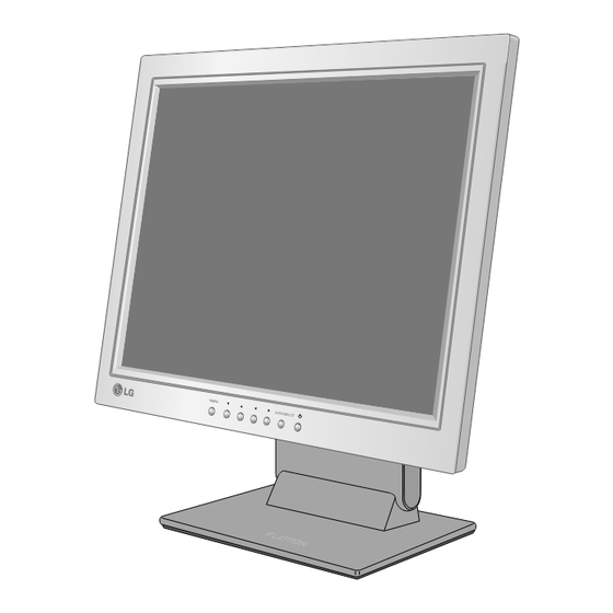
OPERATING INSTRUCTIONS FRONT VIEW REAR VIEW Power Connector D-Sub Signal Connector See front control panel Front Control Panel 1. Power Button 4. AUTO/SELECT Button Use this button to turn the display on or off. Use this button to enter a selection in the On <Power (DPMS) Indicator>... -
Page 6: Wiring Diagram
WIRING DIAGRAM (LG Philips Module) Connector the Power PCB Ass’y and Inverter. Connector Ass’y : P/N: 6631T11012V Connector Ass’y : P/N: 6631T2008G Connector Ass’y : J702 J705 P/N: 6631T12002H J706 J707 P902 Connector Ass’y : P/N: 6631T20015P Connector the Control PCB Ass’y and Power PCB Ass’y. - Page 7 WIRING DIAGRAM (AUO Module) Connector Ass’y : P/N: 6631T11011H Connector Ass’y : Connector Ass’y : P/N: 6631T20008G P/N: 6631T12002H J702 J705 J706 J707 P902 Connector Ass’y : P/N: 6631T20015P - 7 -...
-
Page 8: Block Diagram
BLOCK DIAGRAM ( LG Philips Module) - 8 -... - Page 9 DESCRIPTION OF BLOCK DIAGRAM (LG Philips Module) 1. Scaler One chip IC(GMZAN-2, U201) GMZAN-2 (U201) is one chip IC which it supports four internal function blocks of Video Amp, PLL, A/D converter and Video processor. Video signal (0.7Vp.p) clamped through C207, 208, 209 with matching IC’s proper cut off voltage.
- Page 10 BLOCK DIAGRAM (AUO Module) - 10 -...
- Page 11 DESCRIPTION OF BLOCK DIAGRAM (AUO Module) 1. Scaler One chip IC(GMZAN-2, U201) GMZAN-2 (U201) is one chip IC which it supports four internal function blocks of Video Amp, PLL, A/D converter and Video processor. Video signal (0.7Vp.p) clamped through C207, 208, 209 with matching IC’s proper cut off voltage. This signal is processed as a proper 8 bit digital signal by U201’s amplifying, phase locking, A/D converting, and scaling operations.
-
Page 12: Adjustment
EEPROM. 1. Adjustment for Factory Preset Mode 8) Select PRESET EXIT command and Enter. 1) Run alignment program for LB500J on the IBM compatible PC. 2) Select EEPROM All Init. command and Enter. 3) Display cross hatch pattern at Mode 1. -
Page 13: Troubleshooting Guide
TROUBLESHOOTING GUIDE 1. NO POWER NO POWER (POWER INDICATOR OFF) CHECK POWER CHECK J707 BOARD, AND FIND VOLTAGE OUT A SHORT POINT PIN1&PIN2(12V) AS OPENING PIN4(5V)? EACH POWER LINE CHECK U501 PIN 8 CHECK U803. VOLTAGE (5V) ? CHECK CHECK 5VS LINE U805 Voltage (OPEN CHECK) (5V) ? - Page 14 2. NO RASTER (OSD IS NOT DISPLAYED) – INVERTER NO RASTER (OSD IS NOT DISPLAYED) J705 PIN1 CHECK POWER BOARD 12V? CHECK MICOM INV J705 PIN8 ON/OFF PORT. 1. CONFIRM BRIGHTNESS OSD CONTRL STATE. J705 PIN7 2. CHECK MICOM DIM-ADJ PORT CHECK PULSE AS...
- Page 15 PIN66 IS 48KHz H-SYNC? CONNECTION LINE PIN70 IS 60Hz V-SYNC? FROM U201 TO J402 PIN69 IS 48KHz DEN? IS PULSE APPEARED AT SIGNAL PINS? (LG Philips Module & Hydis Module) CHECK J402 PIN74, PIN1 U401/U411 U805 3.3V? PIN31 IS 65MHz CLOCK?
- Page 16 4. NO RASTER (OSD IS DISPLAYED) – gmZAN2 NO RASTER (OSD IS DISPLAYED) U201 POWER PIN CHECK U802, U806 3.3V? 1. CHECK PC CHECK 2. CHECK SIGNAL CABLE R,G,B INPUT? U201 PIN 87, 91, 95 & D-SUB CONNECTOR LINE CHECK CHECK H-SYNC LINE H-SYNC INPUT (D-SUB U701 MICOM...
-
Page 17: Printed Circuit Board
PRINTED CIRCUIT BOARD LG Philips Module 1. MAIN BOARD (Component Side) L803 R706 R209 C256 C207 C201 R707 R210 C255 R701 C202 C208 R702 R810 C254 R208 R703 C717 C801 C209 C203 R704 C821 D704 D703 R705 R811 RA501 U803... - Page 18 AUO Module 3. MAIN BOARD (Component Side) L803 R706 R209 C256 :2002.02.07 DATE C207 R707 C201 R210 C255 MODEL:LB500J-AU R701 C717 C208 C202 R702 R810 C254 R208 R703 C209 C203 C801 R704 C821 D704 D703 R705 C226 L707 J705 L204...
-
Page 19: Exploded View Parts
- 19 -... -
Page 20: Exploded View Parts List
EXPLODED VIEW PARTS LIST Description Ref. No. Part No. CABINET ASSEMBLY, LB500J BRAND 3090TKL038 3091TKL039B LCD(LIQUID CRYSTAL DISPLAY), LM150X05 C3 LG PHILPS TFT COLOR (LB500J-EL) 6304FLP016A LCD(LIQUID CRYSTAL DISPLAY), L150X3M AU TFT COLOR (LB500J-EU) 6304FAU004A BACK COVER ASSEMBLY, LB500J 3808TKL029A 3809TKL026A TILT SWIVEL ASSEMBLY, LB500J . -
Page 21: Replacement Parts List
REPLACEMENT PARTS LIST CAUTION: BEFORE REPLACING ANY OF THESE COMPONENTS, READ CAREFULLY THE SAFETY PRECAUTIONS IN THIS MANUAL. * NOTE SAFETY Mark AL ALTERNATIVE PARTS DATE: 2002. 2. 23. DATE: 2002. 2. 23. *S *AL LOC. NO. PART NO. DESCRIPTION / SPECIFICATION *S *AL LOC. - Page 22 0 OHM 1/10 W 5% 1608 R/TP R501 0RJ4701D677 4.7K OHM 1/10 W 5% 1608 R/TP R722 0RJ1001D677 1K OHM 1/10 W 5% 1608 R/TP (LB500J-EL) R502 0RJ4701D677 4.7K OHM 1/10 W 5% 1608 R/TP R722 0RJ0000D677 0 OHM 1/10 W 5% 1608 R/TP (LB500J-EU)
- Page 23 DATE: 2002. 2. 23. DATE: 2002. 2. 23. *S *AL LOC. NO. PART NO. DESCRIPTION / SPECIFICATION *S *AL LOC. NO. PART NO. DESCRIPTION / SPECIFICATION RA501 0RHZTCZ001A 100 OHM 1/16 W 5% 3215 R/TP CH 0RJ3301D677 3.3K OHM 1/10 W 5% 1608 R/TP RA502 0RHZTCZ001A 100 OHM 1/16 W 5% 3215 R/TP CH...
-
Page 24: Pin Configuration
PIN CONFIGURATION CAT24WC08J-TE13 8P BLOCK DIAGRAM DIP Package(p) SOIX Package(J) EXTERNAL LOAD V CC V CC SENSE AMPS D OUT SHIFT REGISTERS V SS V SS V CC COLUMN V SS WORD ADDRESS DECODERS BUFFERS TSSOP Package(U) START/STOP LOGIC V CC E PROM XDEC V SS... -
Page 25: Schematic Diagram
SCHEMATIC DIAGRAM (LG Philips Module) 1. GMZAN2 - 25 -... - Page 26 2. LVDS - 26 -...
- Page 27 3. MICOM - 27 -...
- Page 28 4. POWER - 28 -...
- Page 29 5. CONNECTOR & JACKS - 29 -...
- Page 30 6. KEY PART - 30 -...
- Page 31 SCHEMATIC DIAGRAM (AUO Module) 1. GMZAN2 - 31 -...
- Page 32 2. LVDS - 32 -...
- Page 33 3. MICOM - 33 -...
- Page 34 4. POWER - 34 -...
- Page 35 5. CONNECTOR & JACKS - 35 -...
- Page 36 6. KEY PART - 36 -...
- Page 37 Feb. 2002 P/NO : 3828TSL083A Printed in Korea...
Need help?
Do you have a question about the LB500J and is the answer not in the manual?
Questions and answers