Table of Contents
Advertisement
Advertisement
Table of Contents

Related Manuals for Sylvania LD370SS8


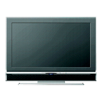
Summary of Contents for Sylvania LD370SS8
- Page 1 SERVICE MANUAL 37″ LCD TV/DVD LD370SS8...
- Page 2 IMPORTANT SAFETY NOTICE Proper service and repair is important to the safe, reliable operation of all Funai Equipment. The service procedures recommended by Funai and described in this service manual are effective methods of performing service operations. Some of these service special tools should be used when and as recommended.
-
Page 3: Table Of Contents
TABLE OF CONTENTS Specifications ................1-1 Laser Beam Safety Precautions . -
Page 4: Specifications
SPECIFICATIONS < LCD TV Section > < TUNER / NTSC > ANT. Input ---------------------- 75 ohm Unbal., F type Description Condition Unit Nominal Limit 1. AFT Pull-in Range ±2.3 ±2.1 TV.ch.4 dBµ 2. Syncronizing Sens. CA.ch.31 dBµ CA.ch.87 dBµ < TUNER / ATSC > Description Condition Unit... - Page 5 <DVD Section> < DVD > Description Condition Unit Nominal Limit 1. Horizontal Resolution (TDV-540 TIT.2 CHP.16) Line 2. Video S/N (TDV-540 TIT.2 CHP.6) 3. Audio Distortion (LPCM 48 kHz, W/LPF) 0.03 0.07 (PTD 1-NOR TIT.1 CHP.1) L, 20 Hz 4. Audio freq. response (LPCM 48 kHz) R, 20 Hz +4/-5 (PTD 1-NOR TIT.1 CHP.5 -- 10)
-
Page 6: Laser Beam Safety Precautions
LASER BEAM SAFETY PRECAUTIONS This DVD player uses a pickup that emits a laser beam. Do not look directly at the laser beam coming from the pickup or allow it to strike against your skin. The laser beam is emitted from the location shown in the figure. When checking the laser diode, be sure to keep your eyes at least 30 cm away from the pickup lens when the diode is turned on. -
Page 7: Important Safety Precautions
IMPORTANT SAFETY PRECAUTIONS Prior to shipment from the factory, our products are strictly inspected for recognized product safety and electrical codes of the countries in which they are to be sold. However, in order to maintain such compliance, it is equally important to implement the following precautions when a set is being serviced. - Page 8 3. Design Alteration Warning - Do not alter or add 7. Product Safety Notice - Some electrical and to the mechanical or electrical design of this TV mechanical parts have special safety-related receiver. Design alterations and additions, characteristics which are often not evident from including, but not limited to circuit modifications visual inspection, nor can the protection they give and the addition of items such as auxiliary audio...
- Page 9 Precautions during Servicing A. Parts identified by the # symbol are critical for safety. Replace only with part number specified. B. In addition to safety, other parts and assemblies are specified for conformance with regulations applying to spurious radiation. These must also be replaced only with specified replacements.
- Page 10 Safety Check after Servicing Examine the area surrounding the repaired location for damage or deterioration. Observe that screws, parts and wires have been returned to original positions. Afterwards, perform the following tests and confirm the specified values in order to verify compliance with safety standards. 1.
-
Page 11: Standard Notes For Servicing
STANDARD NOTES FOR SERVICING Circuit Board Indications Pb (Lead) Free Solder 1. The output pin of the 3 pin Regulator ICs is Pb free mark will be found on PCBs which use Pb indicated as shown. free solder. (Refer to figure.) For PCBs with Pb free mark, be sure to use Pb free solder. - Page 12 around the flat pack-IC to protect other parts from With Soldering Iron: damage. (Fig. S-1-2) 1. Using desoldering braid, remove the solder from 3. The flat pack-IC on the CBA is affixed with glue, so all pins of the flat pack-IC. When you use solder be careful not to break or damage the foil of each flux which is applied to all pins of the flat pack-IC, pin or the solder lands under the IC when...
- Page 13 2. Installation With Iron Wire: 1. Using desoldering braid, remove the solder from 1. Using desoldering braid, remove the solder from all pins of the flat pack-IC. When you use solder the foil of each pin of the flat pack-IC on the CBA flux which is applied to all pins of the flat pack-IC, so you can install a replacement flat pack-IC more you can remove it easily.
- Page 14 Instructions for Handling Semi- conductors Electrostatic breakdown of the semi-conductors may occur due to a potential difference caused by electrostatic charge during unpacking or repair work. 1. Ground for Human Body Be sure to wear a grounding band (1 MΩ) that is properly grounded to remove any static electricity that may be charged on the body.
-
Page 15: Cabinet Disassembly Instructions
CABINET DISASSEMBLY INSTRUCTIONS 1. Disassembly Flowchart Removal Step/ Remove/*Unhook/ This flowchart indicates the disassembly steps for the Loc. Part Fig. Unlock/Release/ cabinet parts, and the CBA in order to gain access to Note Unplug/Unclamp/ item(s) to be serviced. When reassembling, follow the Desolder steps in reverse order. - Page 16 Reference Notes Note: (1) Order of steps in procedure. When reassembling, 1. CAUTION 1: Electrostatic breakdown of the laser follow the steps in reverse order. These numbers diode in the optical system block may occur as a are also used as the Identification (location) No. of potential difference caused by electrostatic charge parts in figures.
- Page 17 [4] Rear Cabinet (S-4) (S-4) (S-5) (S-4) (S-7) [6] DVD Cover (S-5) (S-4) (S-6) (S-1) (S-4) [5] Function CBA (S-4) [3] Stand Cover [2] Stand Hinge [1] Stand Base Plate (S-2) (S-2) (S-2) (S-3) (S-2) Fig. D1 A74G0DC...
- Page 18 (S-8) [7] DVD Main CBA Unit (S-9) [8] DVD Mechanism (S-10) [9] DVD Holder Remove two screws A, then short the three short lands by soldering as shown in View for A. Chassis Cover Screws A Pin A Either of two places View for A FPC Cable Hole A...
- Page 19 [14] Digital Main CBA Unit [12] Jack Earth Plate Holder(D) (S-15) (S-14) (S-13) (N-1) (S-16) Shield Plate (S-11) [13] Shield (S-16) (S-12) (S-11) [11] Power Supply CBA (S-8) (S-12) (S-12) (S-11) (S-11) [10] Chassis Bracket Fig. D3 A74G0DC...
- Page 20 (S-20) [18] Panel Holder (S-20) (S-21) [16] Jack CBA [15] Jack Holder (A) (S-17) (S-18) (S-19) (S-20) (S-19) (S-14) (S-21) (S-20) (S-19) [17] Inverter CBA (S-19) Fig. D4 A74G0DC...
- Page 21 [24] Front Cabinet [20] LCD Module Assembly [23] Speaker (S-23) (S-23) (S-23) (S-26) (S-24) [21] LED CBA (S-23) (S-25) [22] IR Sensor (S-26) (S-22) (S-23) [23] Speaker [19] T-CON CBA Fig. D5 A74G0DC...
- Page 22 TV Cable Wiring Diagram DVD Mechanism DVD Main Jack CBA CBA Unit CN7501 To LCD Module CN201 CN301 Assembly CN801 CN601 CN401 CN9002 CN9001 Function CBA CN9005 CN9003 CN102 T-CON CBA To LCD Module Assembly Digital Main CBA Unit Inverter CBA CN3018 CN3023 CN1300...
-
Page 23: Electrical Adjustment Instructions
ELECTRICAL ADJUSTMENT INSTRUCTIONS General Note: “CBA” is abbreviation for How to set up the service mode: “Circuit Board Assembly.” Service mode: Note: Electrical adjustments are required after 1. Use the service remote control unit. replacing circuit components and certain mechanical parts. It is important to perform 2. - Page 24 1. Purity Check Mode 2. VCOM Adjustment This mode cycles through full-screen displays of red, *This adjustment is required when reparing T-CON green, blue, and white to check for non-active pixels. CBA. 1. Enter the Service mode. Test Point Adj. Point 2.
- Page 25 The following adjustment normally are not attempted in 5. [CUTOFF] the field. Only when replacing the LCD Panel then adjust Press [3] button to select “COB” for Blue Cutoff as a preparation. adjustment. Press [1] button to select “COR” for Red Cutoff adjustment.
-
Page 26: How To Initialize The Lcd Tv/Dvd
HOW TO INITIALIZE THE LCD TV/DVD To put the program back at the factory-default, initialize the LCD TV/DVD using the following procedure. < DVD Section > < LCD TV Section > 1. Press [1], [2], [3], [4], and [INFO] buttons on the 1. -
Page 27: Firmware Renewal Mode
FIRMWARE RENEWAL MODE 1. Turn the power on and press [EJECT] button on the 5. After programming is finished, the disc will be remote control unit to put the LCD TV/DVD into ejected automatically. Fig. e appears on the screen DVD mode. -
Page 28: Block Diagrams
BLOCK DIAGRAMS < LCD TV Section > System Control Block Diagram A74G0BLS... - Page 29 Video Block Diagram A74G0BLV...
- Page 30 Audio-1 Block Diagram A74G0BLA1...
- Page 31 Audio-2 Block Diagram A74G0BLA2...
- Page 32 Digital Signal Process Block Diagram A74G0BLD...
- Page 33 Inverter Block Diagram A74G0BLINV...
- Page 34 Power Supply Block Diagram A74G0BLP...
- Page 35 BLOCK DIAGRAMS < DVD Section > System Control / Servo Block Diagram A74G0BLSD...
- Page 36 DVD Digital Signal Process Block Diagram A74G0BLDD...
-
Page 37: Schematic Diagrams / Cba's And Test Points
SCHEMATIC DIAGRAMS / CBA’S AND TEST POINTS Standard Notes WARNING Many electrical and mechanical parts in this chassis have special characteristics. These characteristics often pass unnoticed and the protection afforded by them cannot necessarily be obtained by using replacement components rated for higher voltage, wattage, etc. - Page 38 LIST OF CAUTION, NOTES, AND SYMBOLS USED IN THE SCHEMATIC DIAGRAMS ON THE FOLLOWING PAGES: 1. CAUTION: CAUTION: FOR CONTINUED PROTECTION AGAINST RISK OF FIRE, REPLACE ONLY WITH SAME TYPE_A,_V FUSE. ATTENTION: UTILISER UN FUSIBLE DE RECHANGE DE MÊME TYPE DE_A,_V. 2.
- Page 39 Power Supply 1/3 Schematic Diagram < LCD TV Section > NOTE: The voltage for parts in hot circuit is measured using hot GND as a common terminal. VOLTAGE CHART CN301 Pin No. Voltage 12.3 12.3 15.7 33.1 10-3 A74G0SCP1...
- Page 40 Power Supply 2/3 Schematic Diagram < LCD TV Section > NOTE: The voltage for parts in hot circuit is measured using hot GND as a common terminal. VOLTAGE CHART CN302 Pin No. Voltage 10-4 A74G0SCP2...
- Page 41 Power Supply 3/3 Schematic Diagram < LCD TV Section > NOTE: The voltage for parts in hot circuit is measured using hot GND as a common terminal. VOLTAGE CHART CN303 Pin No. Voltage 10-5 A74G0SCP3...
- Page 42 Inverter Schematic Diagram < LCD TV Section > VOLTAGE CHART CN552 CAUTION ! Pin No. Voltage Fixed voltage (or Auto voltage selectable) power supply circuit is used in this unit. NOTE: CAUTION ! : For continued protection against risk of fire, If Main Fuse (F501) is blown , check to see that all components in the power supply The voltage for parts in hot circuit is measured using replace only with same type 4 A, 125V fuse.
- Page 43 Jack Schematic Diagram < LCD TV Section > VOLTAGE CHART CN7501 Pin No. Voltage 10-7 A74G0SCJ...
- Page 44 Function Schematic Diagram < LCD TV Section > VOLTAGE CHART CN102 Pin No. Voltage 10-8 A74G0SCF...
- Page 45 IR Sensor & LED Schematic Diagram < LCD TV Section > A74G0SCIR 10-9...
- Page 46 Digital Main 1/10 Schematic Diagram < LCD TV Section > 10-10 A74G0SCD1...
- Page 47 Digital Main 2/10 Schematic Diagram < LCD TV Section > 1 NOTE: The order of pins shown in this diagram is different from that of actual IC3015. IC3015 is divided into four and shown as IC3015 (1/4) ~ IC3015 (4/4) in this Digital Main Schematic Diagram Section. 10-11 A74G0SCD2...
- Page 48 Digital Main 3/10 Schematic Diagram < LCD TV Section > 1 NOTE: The order of pins shown in this diagram is different from that of actual IC3015. IC3015 is divided into four and shown as IC3015 (1/4) ~ IC3015 (4/4) in this Digital Main Schematic Diagram Section. 10-12 A74G0SCD3...
- Page 49 Digital Main 4/10 Schematic Diagram < LCD TV Section > 1 NOTE: The order of pins shown in this diagram is different from that of actual IC3015. IC3015 is divided into four and shown as IC3015 (1/4) ~ IC3015 (4/4) in this Digital Main Schematic Diagram Section. A74G0SCD4 10-13...
- Page 50 Digital Main 5/10 Schematic Diagram < LCD TV Section > 1 NOTE: The order of pins shown in this diagram is different from that of actual IC3015. IC3015 is divided into four and shown as IC3015 (1/4) ~ IC3015 (4/4) in this Digital Main Schematic Diagram Section. A74G0SCD5 10-14...
- Page 51 Digital Main 6/10 Schematic Diagram < LCD TV Section > A74G0SCD6 10-15...
- Page 52 Digital Main 7/10 Schematic Diagram < LCD TV Section > A74G0SCD7 10-16...
- Page 53 Digital Main 8/10 Schematic Diagram < LCD TV Section > 10-17 A74G0SCD8...
- Page 54 Digital Main 9/10 Schematic Diagram < LCD TV Section > A74G0SCD9 10-18...
- Page 55 Digital Main 10/10 Schematic Diagram < LCD TV Section > 10-19 A74G0SCD10...
- Page 56 DVD Main 1/3 Schematic Diagram < DVD Section > 1 NOTE: Either IC461 or IC462 is used for DVD MAIN CBA UNIT. A74G0SCDV1 10-20...
- Page 57 DVD Main 2/3 Schematic Diagram < DVD Section > A74G0SCDV2 10-21...
- Page 58 DVD Main 3/3 Schematic Diagram < DVD Section > A74G0SCDV3 10-22...
- Page 59 Power Supply CBA Top View Because a hot chassis ground is present in the power NOTE: supply circuit, an isolation transformer must be used. The voltage for parts in hot circuit is measured using Also, in order to have the ability to increase the input hot GND as a common terminal.
- Page 60 Power Supply CBA Bottom View Because a hot chassis ground is present in the power NOTE: supply circuit, an isolation transformer must be used. The voltage for parts in hot circuit is measured using Also, in order to have the ability to increase the input hot GND as a common terminal.
- Page 61 Inverter CBA Top View NOTE: The voltage for parts in hot circuit is measured using hot GND as a common terminal. CAUTION ! Because a hot chassis ground is present in the power Fixed voltage (or Auto voltage selectable) power supply circuit is used in this unit. supply circuit, an isolation transformer must be used.
- Page 62 Inverter CBA Bottom View NOTE: The voltage for parts in hot circuit is measured using hot GND as a common terminal. CAUTION ! Because a hot chassis ground is present in the power Fixed voltage (or Auto voltage selectable) power supply circuit is used in this unit. supply circuit, an isolation transformer must be used.
- Page 63 Jack CBA Top View BA71F0F01022-4 10-27...
- Page 64 Jack CBA Bottom View PIN 6 OF PIN 8 OF PIN 9 OF PIN 14 OF CN7501 CN7501 CN7501 CN7501 PIN 5 OF PIN 3 OF PIN1 OF CN7501 CN7501 CN7501 10-28 BA71F0F01022-4...
- Page 65 Function CBA Top View Function CBA Bottom View BA71F0F01022-2 10-29...
- Page 66 IR Sensor CBA Top View LED CBA Top & Bottom View BA71F0F01022-5 IR Sensor CBA Bottom View BA71F0F01022-3 10-30...
- Page 67 WAVEFORMS < LCD TV SECTION > WF1 ~ WF7 = Waveforms to be observed at Waveform check points. (Shown in Schematic Diagram.) Input: NTSC Color Bar Signal (with 1kHz Audio Signal) Pin 1 of CN7501 Pin 5 of CN7501 CVBS 0.2V 20µs VIDEO-Pb...
-
Page 68: Waveforms
WAVEFORMS < DVD SECTION > WF8 ~ WF13 = Waveforms to be observed at Waveform check points. (Shown in Schematic Diagram.) Input: NTSC Color Bar Signal (with 1kHz Audio Signal) DVD Video (Power on (Stop) MODE) Pin 9 of CN201 Pin 5 of CN201 WF11 DVD-AUDIO(L) -
Page 69: Wiring Diagram
WIRING DIAGRAM < LCD TV SECTION > DVD-SPDIF DVD-DISC-OUT DVD-DISC-IN PROTECT4 DVD-AUDIO(R) DVD-AUDIO(L) DVD-Pr DVD-Pb DVD-Y DVD-REMOTE DVD-SDATA DVD-PWR-REQ DVD-CS DVD-SCLK DVD-AUDIO-MUTE LED-CONT 12-1 A74G0WI... - Page 70 WIRING DIAGRAM < DVD SECTION > DVD-Pr DVD-ON+5V 20 CD/DVD 19 DVD-Pb D 18 A 17 DVD-Y C 16 B 15 NU 14 VREF 13 DVD-AUDIO(L) NU 12 DVD-AUDIO-MUTE GND 11 DVD-AUDIO(R) CD-LD 10 GND(LD) 9 DVD-SPDIF DVD-LD 8 PD-MONI 7 GND(DVD-PD) 6 GND(CD-PD) 5 TS(-) 4...
-
Page 71: System Control Timing Charts
SYSTEM CONTROL TIMING CHARTS Disc In ~ Play/Play ~ Disc Out Disc Disc Disc Disc Play Rotation Stop 3.3V Disc IN (TL221) 1.65V Sled Drive (TP303) 1.65V Disc Drive (TP301) 1.65V Focus Drive (TP304) Tracking Drive 1.65V (TP302) 13-1 A7420TI... -
Page 72: Lead Identifications
LEAD IDENTIFICATIONS KTA1267-GR-AT/P 2SC2120-(O, Y) (TE2 F T) 2SA1887(F) KTC2026-Y/P 2SD400(F) KTA1281Y-AT/P KTC3199-GR-AT/P B C E B C E E C B E C B R2A11011FP KIA431-AT/P LV1115M-TLE-E BD5422EFS-E2 OZ9966SN-B1-0-TR/SSO R A K 2SK3568(Q) 2SK3561(Q) LD1117V BA10324AF-E2 1: Vin 2: Vo 3: GND 1 2 3 G D S... -
Page 73: Exploded Views
EXPLODED VIEWS Cabinet CL7501 Jack CBA CLN102 T-CON SP801 CL3007 Digital Main CLN801 Function CBA CBA Unit LED CBA CLN101 CLN802 IR Sensor Power Supply SP802 LCD Module Assembly DVD Main Inverter CBA CBA Unit L3-10 AC501 See Electrical Parts List for parts with this mark. - Page 74 Packing Some Ref. Numbers are not in sequence. Tape Packing Tape Packing Tape Packing Tape Packing Tape Packing Tape Packing Tape Packing Tape PP Band 15-2 A74G0PEX...
-
Page 75: Mechanical Parts List
MECHANICAL PARTS LIST PRODUCT SAFETY NOTE: Products marked with a Ref. No. Description Part No. # have special characteristics important to safety. L3-10 SCREW P-TIGHT M3X8 BIND HEAD+ GBJP3080 Before replacing any of these components, read SCREW P-TIGHT 3X10 BIND HEAD+ GBJP3100 carefully the product safety notice in this service SCREW B-TIGHT 3X10 BIND HEAD+ BLK... -
Page 76: Electrical Parts List
ELECTRICAL PARTS LIST PRODUCT SAFETY NOTE: Products marked with a Ref. No. Description Part No. # have special characteristics important to safety. C605 CERAMIC CAP .(AX) B K 0.027µF/50V CA1J273TU011 Before replacing any of these components, read C606 FILM CAP .(P) 0.1µF/50V J CMA1JJS00104 carefully the product safety notice in this service C608... - Page 77 Ref. No. Description Part No. Ref. No. Description Part No. C851 ELECTROLYTIC CAP . 10µF/50V M CE1JMASDL100 D647 SCHOTTKY BARRIER DIODE SB240-B/P NDQZ000SB240 C857 ELECTROLYTIC CAP . 100µF/16V M CE1CMASDL101 D649 ZENER DIODE MTZJT-7733B QDTB00MTZJ33 C859 ELECTROLYTIC CAP . 47µF/25V M CE1EMASDL470 D650 ZENER DIODE MTZJT-776.2B...
- Page 78 Ref. No. Description Part No. Ref. No. Description Part No. CARBON RES. 1/4W J 4.7k Ω Q602# TRANSISTOR 2SC2120-O(TE2 F T) QQS02SC2120F R654 RCX4JATZ0472 CHIP RES. 1/10W F 1.0k Ω Q631 TRANSISTOR KTC3199-GR-AT/P NQS4KTC3199P R655 RRXAFR5H1001 CARBON RES. 1/4W J 4.7k Ω Q632# PNP TRANSISTOR POWER 2SA1887(F) QQWZ2SA1887F...
- Page 79 Ref. No. Description Part No. Ref. No. Description Part No. CHIP RES. 1/10W J 10 Ω R859 RRXAJR5Z0100 RESISTORS CHIP RES. 1/10W J 5.1k Ω CHIP RES. 1/10W F 2.7k Ω R860 RRXAJR5Z0512 R114 RRXAFR5H2701 CHIP RES. 1/10W J 3.6k Ω CHIP RES.
- Page 80 JACK CBA Ref. No. Description Part No. Ref. No. Description Part No. IC7001 IC VIDEO ANALOG INTERFACE R2A11011FP QSZBA0RHT066 JACK CBA(MPS-4) ---------- QFP 56PIN Consists of the following: COILS CAPACITORS L7802 PCB JUMPER D0.6-P5.0 JW5.0T C7001 ELECTROLYTIC CAP . 47µF/16V M H7 CE1CMAVSL470 L7803 PCB JUMPER D0.6-P5.0...
- Page 81 Ref. No. Description Part No. Ref. No. Description Part No. CHIP RES. 1/10W J 100 Ω R7788 RRXAJR5Z0101 C1008 CHIP CERAMIC CAP . F Z 2.2µF/10V CHD1AZ30F225 MISCELLANEOUS C1009 CHIP CERAMIC CAP .(1608) B K 0.1µF/50V CHD1JK30B104 C1010 CERAMIC CAP .(AX) F Z 0.1µF/50V CCA1JZTFZ104 JK7501 JACK HPEP SML PCB S PJ-358H...
- Page 82 Ref. No. Description Part No. Ref. No. Description Part No. C1257 CHIP CERAMIC CAP .(1608) CH J 390pF/50V CHD1JJ3CH391 D511 FAST RECOVERY DIODE FE201-6 QDLZ00FE2016 C1261 CERAMIC CAP . SL D 10pF/3KV CCD3FDASL100 D512 SWITCHING DIODE 1SS133(T-77) QDTZ001SS133 C1262 CHIP CERAMIC CAP . B K 1200pF/50V CHD1JK30B122 D513 DIODE 1ZC33(Q)
- Page 83 Ref. No. Description Part No. Ref. No. Description Part No. D1260 SWITCHING DIODE 1SS133(T-77) QDTZ001SS133 Q552 TRANSISTOR KTC3199-GR-AT/P NQS4KTC3199P D1261 SWITCHING DIODE 1SS133(T-77) QDTZ001SS133 Q1001 TRANSISTOR KTC3199-GR-AT/P NQS4KTC3199P D1262 SWITCHING DIODE 1SS133(T-77) QDTZ001SS133 Q1002 TRANSISTOR KTC3199-GR-AT/P NQS4KTC3199P D1263 SWITCHING DIODE 1SS133(T-77) QDTZ001SS133 Q1003 TRANSISTOR KTC3199-GR-AT/P...
- Page 84 Ref. No. Description Part No. Ref. No. Description Part No. CHIP RES. 1/10W J 5.1k Ω CHIP RES. 1/10W J 100k Ω R1002 RRXAJR5Z0512 R1164 RRXAJR5Z0104 CHIP RES. 1/10W J 220k Ω CHIP RES. 1/10W J 20k Ω R1003 RRXAJR5Z0224 R1165 RRXAJR5Z0203 CHIP RES.
- Page 85 Ref. No. Description Part No. Ref. No. Description Part No. CHIP RES. 1/10W F 6.8k Ω R1369 RRXAFR5Z6801 BC1151 PCB JUMPER D0.6-P10.0 JW10.0T CHIP RES. 1/10W J 1M Ω R1370 RRXAJR5Z0105 BC1200 PCB JUMPER D0.6-P10.0 JW10.0T CHIP RES. 1/10W J 1k Ω R1371 RRXAJR5Z0102 BC1201...
- Page 86 Misuse of any trademarks or any other content in this manual is strictly prohibited. Funai shall aggressively enforce its intellectual property rights to the fullest extent of the law. LD370SS8 A74G0UH 2007-06-06...
Need help?
Do you have a question about the LD370SS8 and is the answer not in the manual?
Questions and answers