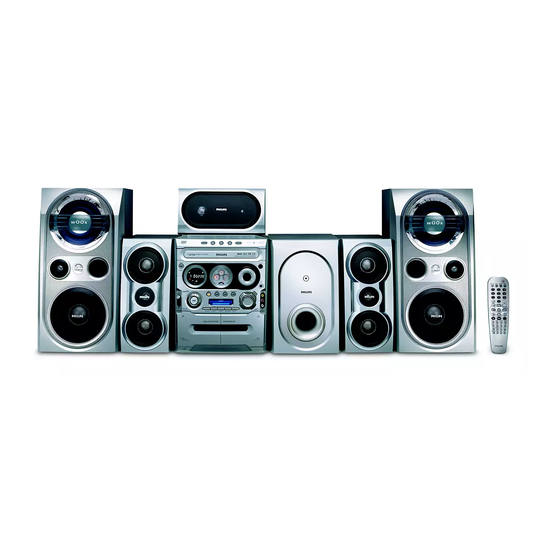
Philips FWD796 Service Manual
Hide thumbs
Also See for FWD796:
- User manual (49 pages) ,
- Service manual (13 pages) ,
- Quick use manual (2 pages)
Table of Contents
Advertisement
Mini System
Service
Service
Service
Service
Service
Service Manual
©
Copyright 2005 Philips Consumer Electronics B.V. Eindhoven, The Netherlands
All rights reserved. No part of this publication may be reproduced, stored in a retrieval system or
transmitted, in any form or by any means, electronic, mechanical, photocopying, or otherwise
without the prior permission of Philips.
Published by SL-ET0519 Service Audio Printed in The Netherlands Subject to modification.
Version 1.0
TABLE OF CONTENTS
Location of PCBs & Specifications .................. 1-2 to 1-3
Measurement Setup & Service Aids ................ 1-4 to 1-5
ESD & Safety Instruction ............................................ 1-6
Lead-Free Information & Service Instruction ............. 1-7
Preparations & Controls & Troubleshooting .. 1-8 to 1-14
Setting Procedure & Repair Instructions ....................... 2
Disassembly Instructions & Service positions .............. 3
Set Block & Wiring Diagram .......................................... 4
Key/Video/Sensor/Phone/Vol /Vu Board ....................... 5
Tuner Board ................................................................... 6
Main Board .................................................................... 7
Power Board .................................................................. 8
Mechanical Exploded View & Parts List ........................ . .9
Subwoofer Part ............................................................ 10
Location of PCBs & Specifications .......................... 10-1
Measurement Setup & Service Position ..... 10-2 to 10-3
Disassembly Instructions & Service Positions ........ 10-4
Set Block & Wiring Diagram ........................ 10-5 to 10-6
Main Board ................................................ 10-7 to 10-11
Power & LED Board ................................ 10-12 to 10-15
Exploded View & Parts List ..................... 10-16 to 10-17
FWD796/
Page
VIDEO CD
CLASS 1
LASER PRODUCT
GB
3141 785 30360
21/21M
Advertisement
Table of Contents

Subscribe to Our Youtube Channel
Related Manuals for Philips FWD796


Summary of Contents for Philips FWD796
- Page 1 LASER PRODUCT © Copyright 2005 Philips Consumer Electronics B.V. Eindhoven, The Netherlands All rights reserved. No part of this publication may be reproduced, stored in a retrieval system or transmitted, in any form or by any means, electronic, mechanical, photocopying, or otherwise without the prior permission of Philips.
-
Page 2: Location Of Printed Circuit Boards
MOTOR1 BOARD KARAOKE BOARD GAME PORT BOARD POWER BOARD HEADPHONE BOARD VERSION VARIATIONS: Type /Versions: FWD796 /21M Features & Board in used: Aux in /CDR in Line Out DIN Out Subwoofer Out Video Out S-Video Out Component Video Out Digital Out... -
Page 3: Specifications
............4 Hz - 44 kHz (96kHz) Output power ..........3640 W PMPO Digital Output ..............Stereo mode (DIN) ......140 W + 140 W RMS ....SPDIF (Sony Philips digital interface) Coaxial Surround mode (1 kHz) ........DIN OUT PCM ..............IEC 60958 ±... -
Page 4: Measurement Setup
MEASUREMENT SETUP Tuner FM Bandpass LF Voltmeter 250Hz-15kHz e.g. PM2534 e.g. 7122 707 48001 RF Generator e.g. PM5326 S/N and distortion meter e.g. Sound Technology ST1700B Use a bandpass filter to eliminate hum (50Hz, 100Hz) and disturbance from the pilottone (19kHz, 38kHz). Tuner AM (MW,LW) Bandpass LF Voltmeter... -
Page 5: Service Aids
SERVICE AIDS ESD Equipment: Service Tools: Universal Torx driver holder .........4822 395 91019 Anti-static table mat - large 1200x650x1.25mm ...4822 466 10953 anti-static table mat - small 600x650x1.25mm ..4822 466 10958 Torx bit T10 150mm ...........4822 395 50456 Anti-static wristband ..........4822 395 10223 Torx driver set T6-T20 .........4822 395 50145 Connectorbox (1M Ω) -
Page 6: Class 1 Laser Product
WAARSCHUWING WARNING Alle IC’s en vele andere halfgeleiders zijn All ICs and many other semi-conductors are gevoelig voor electrostatische ontladingen susceptible to electrostatic discharges (ESD). (ESD). Careless handling during repair can reduce life Onzorgvuldig behandelen tijdens reparatie kan drastically. de levensduur drastisch doen verminderen. When repairing, make sure that you are Zorg ervoor dat u tijdens reparatie via een connected with the same potential as the mass... -
Page 8: Preparations And Controls
PREPARATIONS AND CONTROLS... - Page 9 PREPARATIONS AND CONTROLS...
- Page 10 1-10 PREPARATIONS AND CONTROLS...
- Page 11 1-11 PREPARATIONS AND CONTROLS...
-
Page 12: Functional Overview
1-12 FUNCTIONAL OVERVIEW... - Page 13 1-13 FUNCTIONAL OVERVIEW...
-
Page 14: Troubleshooting
1-14 TROUBLESHOOTING... - Page 15 System, Region code, Tuner, etc. setting procedure 5. Video Out Change 3) Region code change timer reset a) Press "SYSTEM" on R/C button Press below key to reset the timer : Hence in total, reprograming will be done by way of the 1) System Reset b) Select the menu using the "...
-
Page 16: Repair Instructions
REPAIR INSTRUCTIONS... - Page 17 REPAIR INSTRUCTIONS...
-
Page 18: Dismantling Instructions
DISMANTLING INSTRUCTIONS Dismantling of the Cassette Cover Pull out Press and hold it between the tape deck and the cassette door Figure 2 Figure 4 Figure 1 Dismantling the 3CDC Module Dismantling of the Cover Front Display and Cover Front Ornamental (pos 130) 4) Remove the Cover Tray as shown in figure 4. - Page 19 Detaching the Main board and Front Cabinet Assembly from the Bottom/Rear assembly Dismantling of the Rear Panel 1) Release 2 catches 'B' to free the Main board from the Front 1) Loosen 8 screws 'J' to remove the Rear Panel figure 11. Cabinet Assembly as shown in figure 6.
-
Page 20: Service Positions
Service positions Service position A Service position B Note: After re-assembly, it is very important to ensure the wires are properly inserted into their respective sockets and routed not to touch or obstruct any moving parts. Service position C... - Page 21 SET BLOCK DIAGRAM...
- Page 22 SET WIRING DIAGRAM...
-
Page 23: Ftd Display Pin Assignment
FTD DISPLAY PIN ASSIGNMENT KEY / VIDEO / SENSOR / PHONE / VOL / VU BOARD TABLE OF CONTENTS FTD Display Pin Assignment ........... 5-1 FTD Display Pin Connection ........... 5-1 Internal IC Diagram & Pin Description ......5-2 Circuit Diagram ..............5-3 PCB Layout Top View ............ - Page 24 PIN DESCRIPTION INTERNAL BLOCK DIAGRAM VFD CONTROLLER - IC TP6311QH VFD CONTROLLER - IC TP6311QH SG1/KS1 Control SG2/KS2 SG3/KS3 T s i i p SG4/KS4 t f i i t r . ) t Serial Genaral Segment SG5/KS5 Data Input SG6/KS6 Driver/ T s i i p...
-
Page 25: Circuit Diagram - Key Board
CIRCUIT DIAGRAM - KEY BOARD C1805 R284 SW803 C2001 R285 SW804 C2002 R286 TA251 C2003 R287 TA253 C2004 R288 TA255 C2005 R289 TA258 C2006 R291 TA259 C2007 R292 TA260 C2008 R293 TA261 C2009 R294 TA262 C2010 R295 TA263 C2012 R296 TA265 C2013 R297... -
Page 26: Pcb Layout - Key Board (Top)
PCB LAYOUT - KEY BOARD (TOP) C2017 C2018 IC254 LD256 R2042 R2043 R2044 R2045 R2046 RB252 RB253 RB254 RB257 RB803 RB804 SW803 SW804 TA255 TA258 TA259 TA260 TA261 TA262 TA263 TA265 TA266 TA267 TA268 TA269 TA270 TA271 TA272 TA273 TA274 TA276 TA277 TA278... - Page 27 C1805 R2025 PCB LAYOUT - GAME & MIC & PHONE BOARD (TOP VIEW) C2003 R2026 C2004 R2027 C2009 R2029 C2010 R2030 C2016 R2040 C2023 R2041 C2028 R2056 C2032 R2057 C2034 R2062 C2035 R2063 CN202 R2064 CN252 R2066 CN253 R2067 CN254 R2068 CN257 R2071...
- Page 28 PCB LAYOUT - GAME & MIC & PHONE BOARD (BOTTOM VIEW) C2001 C2002 C2005 C2006 C2007 C2008 C2011 C2012 C2013 C2014 C2015 C2019 C2020 C2021 C2024 C2025 C2026 C2027 C2029 C2030 C2031 C2225 C2226 C2227 C2228 ESDC2 D1 ESDC5 D1 IC251 IC255 Q251...
- Page 29 ELECTRIC PARTS - KEY BOARD SW803 9940 000 00871 TACT SW DIA1.7MM SW804 9940 000 00871 TACT SW DIA1.7MM TA280 9940 000 00872 TACT SW 50MA 12V TA281 9940 000 00872 TACT SW 50MA 12V TA282 9940 000 00872 TACT SW 50MA 12V TA283 9940 000 00872 TACT SW 50MA 12V...
- Page 30 TUNER ADJUSTMENT TABLE Waverange Input frequency Input Tuned to Adjust Output Scope/Voltmeter VARICAP ALIGNMENT ± 108MHz 7.5V check 87.5 - 108MHz ± (50kHz grid) 87.5MHz check 1.4V 0.2V ± 1602KHz 7.2V check ± 1.1V 0.2V 531KHz T005 531-1602kHz TUNER BOARD (9940 000 00873) (10kHz grid) ( 21L / 21L / 37S ) FM - RF...
-
Page 31: Tuner Adjustment Table
TUNER ADJUSTMENT TABLE ANT001 R001 R002 R003 R004 C002 R005 C004 R006 C005 R007 C006 R008 C007 R009 C008 R010 C009 R011 C010 R012 C011 R013 C012 R014 C013 R015 C014 R016 C015 R017 C016 R018 C017 R019 C018 R020 C019 R021 C020... -
Page 32: Circuit Diagram - Tuner Board (Top View)
CIRCUIT DIAGRAM - TUNER BOARD (TOP VIEW) ANT001 A2 C010 C029 C043 D001 Q003 T004 C014 C030 C044 D002 T005 C017 C033 C045 D004 R005 T006 C019 C036 C046 IC001 R024 VC001 C004 C024 C037 C047 IF001 R035 VD001 C005 C025 C038 C048... -
Page 33: Pcb Layout - Tuner Board (Bottom View)
PCB LAYOUT - TUNER BOARD (BOTTOM VIEW) C016 C032 D005 R002 R011 R019 R029 R040 VR001 C002 C018 C034 IC001 R003 R012 R020 R030 R046 C006 C020 C035 IC002 R004 R013 R021 R033 T002 C007 C021 C040 Q001 R006 R014 R023 R034 T003... -
Page 34: Tda8920 Internal Ic Diagram
TDA8920 INTERNAL IC DIAGRAM V DDA2 V DDA1 V DDP2 V DDP1 MAIN BOARD STABI PROT BOOT1 RELEASE1 IN1− DRIVER INPUT HIGH SWITCH1 CONTROL STAGE MODULATOR IN1+ OUT1 ENABLE1 HANDSHAKE DRIVER mute SGND1 STABI V SSP1 TEMPERATURE SENSOR TDA8920TH OSCILLATOR MANAGER V DDP2 CURRENT PROTECTION... - Page 35 BLOCK DIAGRAM - MAIN BOARD DVD/CD Motor Motor Driver Video ES6603S T V Display RF Amp 8/16-MB Audio DAC Speakers DRAM Audio ADC ES6698 Microphone In Vibratto-II EEPROM S/PDIF A/V Receiver ROM/Flash VFD Panel VFD Driver IR Remote...
-
Page 36: Circuit Diagram - Main Board
CIRCUIT DIAGRAM - MAIN BOARD C294 R235 C2273 R2205 C295 C2266 R236 R2206 SERVO PART C296 R237 C2274 R2208 C297 R238 C2275 R2209 C801 R240 C2276 R2210 C802 C2277 R241 R2211 C803 R242 C2278 R2212 C804 R243 C2279 R2213 C805 C2280 R244 R2214... - Page 37 CIRCUIT DIAGRAM - MAIN BOARD...
- Page 38 CIRCUIT DIAGRAM MAPPING - MAIN BOARD SERVO PART...
-
Page 39: Circuit Diagram - Tape Part
CIRCUIT DIAGRAM - TAPE PART C701 D701 R726 R7001 C702 D702 R727 R7004 C703 D703 R728 R7005 C704 D704 R729 R7007 C705 D705 R730 R7008 C706 D706 R731 R7009 C707 D707 R732 R7010 C708 D708 R733 R7011 C709 D709 R734 R7012 C710 D710... - Page 40 PCB LAYOUT - MAIN BOARD TOP VIEW...
- Page 41 PCB LAYOUT MAPPING - MAIN BOARD PCB LAYOUT MAPPING - MAIN BOARD TOP VIEW BOTTOM VIEW...
-
Page 42: Pcb Layout - Main Board Bottom View
PCB LAYOUT - MAIN BOARD BOTTOM VIEW R3017 R3018... - Page 43 7-10 7-10 ELECTRIC PARTS - MAIN BOARD CF501 9940 000 00822 RESONATOR 2PIN 600KHZ IC703 4822 209 32919 HEF4952BT CF502 9940 000 00823 RESONATOR 2PIN 700KHZ IC704 4822 209 32919 HEF4952BT IC1011 4822 209 60614 IC NJM2246M IC705 5322 209 11306 HEF4094BT IC201 9940 000 00827...
-
Page 44: Power Board
KA5M02659RN INTERNAL BLOCK DIAGRAM POWER BOARD OUTPUT CONTROL OSCILLATOR DEAD TIME 1.2V CONTROL V CC COMP EA(+) TABLE OF CONTENTS BAND GAP V REF Internal Block Diagram ............8-1 EA(-) REFERENCE Circuit Diagram ..............8-2 0.7MA EA(+) PCB Layout ................8-3 Electrical Parts List .............. -
Page 45: Circuit Diagram - Power Board
CIRCUIT DIAGRAM - POWER BOARD BD901 A1 C908 A2 C919 D1 C953 A4 C963 B5 C978 D4 C988 A3 C998 CN903 A1 D908 D960 IC954 B4 L959 Q954 R903 R914 R951 R961 R973 R983 R993 TR902 BF901 A2 C909 A2 C920 C1 C954 A4 C964 C5... -
Page 46: Pcb Layout - Power Board
PCB LAYOUT - POWER BOARD BD901 C913 C953 C974 C991 CN902 B1 D953 J801 JMP12 C2 JMP30 A1 Q905 R906 R922 R965 R982 R999 C851 C914 C954 C975 C992 CN903 A1 D954 J802 JMP13 D5 JMP31 A1 Q951 R906A R923 R966 R983 RT901... - Page 47 ELECTRIC PARTS - POWER BOARD BD901 9940 000 00931 BRIDGE KBU808 8A 1000V IC901 9940 000 00945 IC 8PIN KA5M02659RN C902 9940 000 00932 COND SAFTY 0.47µF 275V 10% IC902 9940 000 00946 OPTICAL SENSOR 4P C903 9940 000 00932 COND SAFTY 0.47µF 275V 10% IC951 9940 000 00947...
-
Page 48: Mechanical Exploded View
MECHANICAL EXPLODED VIEW SCREW LIST Description SCREW M3.0xP0.5x22mm SCREW T2.0x0.63PxL7mm SCREW L8xP1.06xT3.0mm D=7.5mm SCREW T3.0xL8xP1.06mm,0.47g SCREW M3.0xP0.5x8 SCREW T3.0xL8xP1.06mm SCREW M3.0xP0.5x6,0.5g SCREW T3.0xL8.0xW/@10.0mm SCREW T3.0xL10xP1.06mm SCREW M3x6x0.5P SCREW M3.0xP0.5x10 SCREW T3.0xL10xP1.06mm... - Page 49 3 CDC MODULE 9940 000 00873 TUNER MODULE 9940 000 00917 FAN 60X60X15MM DC 12V 9940 000 00927 TAPE DECK PHILIPS 9940 000 00877 RUBBER φ14XT2MM Note: Only these parts mentioned in the list are 9940 000 00899 COVER TOP...
-
Page 50: Location Of Pc Boards
10-1 LOCATION OF PC BOARDS MAIN BOARD POWER BOARD LED BOARD SPECIFICATIONS SUBWOOFER Subwoofer (not magnetically shielded design) ....................... 6.5" Output Power(10% at 80Hz) ........................100W (4Ω) Reproduction Frequency Response ......................30 Hz-200 Hz Input Sensitivity (Subwoofer In) ........................ 450 mV/rms AC Power ..........................110 - 127V / 220 - 240V Power Consumption ...................... - Page 51 10-2 MEASUREMENT SETUP AUDIO LOAD 3OHM Generator LEVEL DISTORTION METER JK401 JK501 SCOPE...
-
Page 52: Disassembly Instructions
10-3 DISASSEMBLY INSTRUCTIONS Dismantling the Grill Base & Speaker Driver 2. Place the Subwoofer Box as shown in the Picture 2 1. Place the Subwoofer Box as shown in the Picture 1 and loosen 4 screws B to remove the Speaker Driver. and use a screw driver to open the Grill Base. -
Page 53: Service Position
10-4 SERVICE POSITION... - Page 54 10-5 10-5 SUBWOOFER SET BLOCK DIAGRAM...
- Page 55 10-6 10-6 SUBWOOFER SET WIRING DIRGRAM...
- Page 56 10-7 10-7 TDA8920TH INTERNAL IC DIAGRAM VDDP2 VDDP1 STAB1 PROT VDDA2 VDDA1 BOOT1 RELEASE IN1- DRIVER INPUT MODULATOR SWITCH1 CONTROL HIGH STAGE IN1+ OUT1 ENABLE1 HANDSHAKE DRIVER MUTE SUBWOOFER MAIN BOARD SGND1 STAB1 VSSP1 OSDILLATOR TDA8920TH TEMPERATURE SENSOR MANAGER VDDP2 CURRENT PROTECTION MODE MODE...
- Page 57 10-8 10-8 CIRCUIT DIAGRAM - MAIN BOARD C302 D6 C576 R409 C2 C303 D7 C577 R410 C2 C401 C2 C578 R411 B2 C403 B2 C579 R412 A2 C404 A2 C580 R413 C3 C405 C2 C901 R414 C3 C406 B2 C902 R415 B3 CN904 C407 B2...
- Page 58 10-9 10-9 MAIN PCB LAYOUT TOP VIEW C302 B3 CN301 B4 R920 A2 C303 B3 CN501 A2 R921 A2 C401 E1 CN901 A4 R922 E4 C402 E1 CN902 E4 R923 A3 C403 E1 CN904 E4 R924 A3 C404 E1 D301 B2 ZD301 B3 C405 E1 D906 A3...
- Page 59 10-10 10-10 MAIN PCB LAYOUT BOTTOM VIEW C413 C1 R523 B2 C501 B2 R524 A2 C502 A2 R525 C2 C503 C1 R526 C2 C504 B1 R527 B2 C505 B2 R528 A2 C506 A2 R529 C2 C507 C2 R530 B2 C508 B2 R535 D2 C509 B2 R539 D3...
- Page 60 10-11 10-11 ELECTRICAL PARTS - MAIN BOARD C915 996500019963 COND ELECT 3300µF 35V 20% C916 996500019963 COND ELECT 3300µF 35V 20% IC401 994000002064 IC 14P TL074CDT IC501 994000000846 IC 24P TDA8920BTH IC502 994000000846 IC 24P TDA8920BTH JK401 996500022220 DIN JACK 8PIN JK501 994000002062 SPK JACK 6P G-G-B/Bx3...
- Page 61 10-12 10-12 IC-KA7500C INTERNAL IC DIAGRAM POWER + LED BOARDS IC-BA4558D INTERNAL IC DIAGRAM TABLE OF CONTENTS Internal IC Diagram ............. 10-12 Circuit Diagram ............10-13 PCB Layout View ............10-14 Electrical Parts list ............10-15 OUTPUT -INPUT +INPUT...
- Page 62 10-13 10-13 CIRCUIT DIRGRAM - POWER BOARD NTC901C1 BD901 D1 Q901 C901 C902 Q902 Q911 C903 L-45UH-8A Q912 C904 C955 470P-1KV L952 C104P-100V Q951 C907 RB951 Q952 D972 C908 UF3003 +27V T901 Q957 1000U 35V C909 D971 UF3003 Q958 C910 C956 -27V C911...
- Page 63 10-14 10-14 PCB LAYOUT - POWER + LED BOARD BD901 E3 J911 T902 C901 J912 C902 J913 C903 J914 TVR901 D1 C904 J915 ZD901 C1 C907 J916 ZD902 C4 C908 L901 ZD952 A4 C909 L951 ZD953 A1 C910 L952 C911 L957 C913 NTC901D3...
- Page 64 10-15 10-15 ELECTRICAL PARTS - POWER & LED BOARD BD901 9940 000 02065 RECTIFIER GBU4J 4A 600V C903 9940 000 00932 COND SAFTY 0.47µF 275V 125' 10% C904 9940 000 00932 COND SAFTY 0.47µF 275V 125' 10% C909 9940 000 01086 COND DISC 0.01µF 1KV 20% C910 9940 000 01086...
- Page 65 10-16 10-16 MECHANICAL EXPLODED VIEW...
- Page 66 10-17 10-17 MECHANICAL & ACCESSORIES PARTS ELECTRICAL PARTS - MISCELLANEOUS SCREW LIST 9940 000 02072 RUBBER PAD OD20XT4 9940 000 00918 FFC 14P P=1.27MM 220MM SCREW T3xL8xP1.06 9940 000 02074 SPK DRIVER 61/2" 100W 3Ω SCREW T3.5xP1.4xL20 9940 000 00919 FFC 24P P=0.5MM 380MM 9965 000 15949 GRILLE...
Need help?
Do you have a question about the FWD796 and is the answer not in the manual?
Questions and answers