Table of Contents
Advertisement
Quick Links
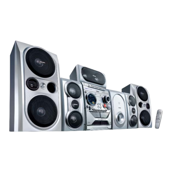
DVD Mini System
©
Copyright 2006 Philips Consumer Electronics B.V. Eindhoven, The Netherlands
All rights reserved. No part of this publication may be reproduced, stored in a retrieval system or
transmitted, in any form or by any means, electronic, mechanical, photocopying, or otherwise without
the prior permission of Philips.
Published by SL 0623 Service Audio
Version 1.0
TABLE OF CONTENTS
Location Of Pc Boards ......................................................... 1-2
Speci cations ....................................................................... 1-3
Measurement Setup ............................................................. 1-4
Service Aids, Safety Instruction, etc ...........................1-5 to 1-7
Connections & Functional Overview......................... 1-8 to 1-11
Troubleshooting ......................................................1-12 to 1-13
Repair Instructions................................................................... 2
Disassembly Instructions & Service positions ......................... 3
Set Block Diagram ................................................................ 4-1
Set Wiring Diagram .............................................................. 4-2
Control Board .......................................................................... 5
Main Board .............................................................................. 6
Tuner Board ............................................................................. 7
Power Board ............................................................................ 8
Mechanical Exploded View & Parts List .................................. 9
Subwoofer Part ...................................................................... 10
Printed in The Netherlands
Subject to modification
FWD798
Page
CLASS 1
© 3141 785 30890
/37/55/98
VIDEO CD
Advertisement
Table of Contents

Subscribe to Our Youtube Channel
Related Manuals for Philips FWD798/37


Summary of Contents for Philips FWD798/37
- Page 1 LASER PRODUCT © Copyright 2006 Philips Consumer Electronics B.V. Eindhoven, The Netherlands All rights reserved. No part of this publication may be reproduced, stored in a retrieval system or transmitted, in any form or by any means, electronic, mechanical, photocopying, or otherwise without the prior permission of Philips.
-
Page 2: Location Of Pc Boards
LOCATION OF PC BOARDS MAIN PCB CONTROL PCB TUNER PCB POWER PCB VERSION VARIATION: Type /Versions FWD798 Features & Board in used Main PCB (No ECO Power<10W) Main PCB (ECO Power<10W) Power (Dual Voltage) Power (120V only) AC line Cord (datachable) AC line Cord (fixed) - Page 3 Specifications AMPLIFIER SECTION SPEAKERS Output power ..........9800 W PMPO Front speakers Stereo mode ............750 W RMS System ............. 3-way, Bass reflex Frequency Response ....180 Hz - 16 kHz / ± 3 dB Impedance ..............Ω Signal-to-Noise Ratio ......> 60dB (A-weighted) Speaker drivers ..........
-
Page 4: Measurement Setup
MEASUREMENT SETUP Tuner FM Bandpass LF Voltmeter 250Hz-15kHz e.g. PM2534 e.g. 7122 707 48001 RF Generator e.g. PM5326 S/N and distortion meter e.g. Sound Technology ST1700B Use a bandpass filter to eliminate hum (50Hz, 100Hz) and disturbance from the pilottone (19kHz, 38kHz). Tuner AM (MW,LW) Bandpass LF Voltmeter... - Page 5 SERVICE AIDS ESD Equipment: Service Tools: Anti-static table mat - large 1200x650x1.25mm ...4822 466 10953 Universal Torx driver holder .........4822 395 91019 anti-static table mat - small 600x650x1.25mm ..4822 466 10958 Torx bit T10 150mm ...........4822 395 50456 Anti-static wristband ..........4822 395 10223 Torx driver set T6-T20 .........4822 395 50145 Connectorbox (1M ..........4822 395 11307...
-
Page 6: Laser Product
WAARSCHUWING WARNING Alle IC’s en vele andere halfgeleiders zijn All ICs and many other semi-conductors are gevoelig voor electrostatische ontladingen susceptible to electrostatic discharges (ESD). (ESD). Careless handling during repair can reduce life Onzorgvuldig behandelen tijdens reparatie kan drastically. de levensduur drastisch doen verminderen. When repairing, make sure that you are Zorg ervoor dat u tijdens reparatie via een connected with the same potential as the mass... - Page 7 To avoid wear-out of tips switch off un-used equipment, or reduce heat. • Mix of lead-free solder alloy / parts with leaded solder alloy / parts is possible but PHILIPS recommends strongly to avoid mixed solder alloy types (leaded and lead-free).
- Page 8 1 - 8 CONNECTIONS...
- Page 9 1 - 9 CONNECTIONS...
- Page 10 1 - 10 CONNECTIONS...
- Page 11 1 - 11 FUNCTIONAL OVERVIEW...
- Page 12 1 - 12 FUNCTIONAL OVERVIEW & PREPARATIONS...
- Page 13 1 - 13...
- Page 14 System, Region code, Tuner, etc. setting procedure 5. Video Out Change 3) Region code change timer reset a) Press "SYSTEM" on R/C button Press below key to reset the timer : Hence in total, reprograming will be done by way of the 1) System Reset b) Select the menu using the "...
- Page 17 DISMANTLING INSTRUCTIONS Dismantling the DVD Module Dismantling of the Cover Front Display 1) Remove the Volume knobs as stated in Dismantling the Cover Front Display in Figure 7. 1) Loosen the 4 screws at top cover , 2 screws at slide Cover 2) Loosen 2 screws at the bottom of front panel.
-
Page 18: Control Board
Dismantling of the Control Board & Cassette Module Dismantling of the Power Board 1) Loosen 4 screws 'J' to remove the Power Board figure 13. 1) Loosen 19 screws 'H' to remove the control board figure 11. 2) Loosen 4 screws 'I' to remove the Cassette Module figure 12. Figure 13 Figure 12... -
Page 19: Service Positions
Service positions Service position A Service position B Note: After re-assembly, it is very important to ensure the wires are properly inserted into their respective sockets and routed not to touch or obstruct any moving parts. Service position C... - Page 20 BLOCK DIAGRAM Control system Tuner system...
- Page 21 WIRING DIAGRAM CN903 LOADER POWER PCB MAIN PCB SUBWOOFER FOR FWD798 CONTROL MODEL ONLY TAPE DECK TUNER PCB...
- Page 22 FTD DISPLAY PIN ASSIGNMENT (3G 10G) (3G 10G) CONTROL BOARD 10G 11G TABLE OF CONTENTS j ,p j ,p j ,p j ,p j ,p j ,p j ,p j ,p FTD Display Pin Assignment ........... 5-1 Pin Connection ..............5-1 Circuit Diagram ..............
- Page 23 CIRCUIT DIAGRAM: CONTROL PCB C2501 C2512 C2525 C5017 C852 D2506 IC2501 Q2506 R2510 R2521 R2536 R2548 R2560 RB909 TA2506 D5 TA2517 D5 ZD2501 C4 C2502 C2513 C2526 C5018 CN257 D2507 IC2502 Q2507 R2511 R2522 R2537 R2549 R2561 SN2501 B4 TA2507 D5 TA2518 D5 ZD2502 C4 C2503...
- Page 24 PCB LAYOUT:KEY / SW / MOTOR PCB C851 CN803A A1 CN806A A2 CN808A A2 J801 J803 J805 RB257 B2 RB804 B1 SW802 A2 SW804 B2 C852 CN804A A2 CN807A A2 CN810A A1 J802 J804 J806 RB803 B1 SW801 A1 SW803 B2...
- Page 25 PCB LAYOUT - CONTROL PCB (TOP VIEW) C2510 JK302 JP2508 A3 JP2517 B3 JP2527 A2 JP2536 A2 JP2545 B2 JP2554 A2 JP2563 A2 JP2572 A2 JP2588 A1 JP2597 B2 JP2606 B1 Q2508 TA2504 B2 TA2513 A2 C2514 JK551 JP2509 A3 JP2518 A3 JP2528 A2 JP2537 A2...
- Page 26 PCB LAYOUT - CONTROL PCB (BOTTOM VIEW) C2501 A2 C2508 A1 C2521 B2 C2529 B2 C5019 A1 C5308 A1 D2505 B2 FB2501 A3 Q2503 A2 R2505 B3 R2512 A2 R2519 A2 R2526 A2 R2538 A2 R2546 B3 R2553 B2 R2561 B2 ZD2503 B3 C2502 A2 C2509 A1...
- Page 27 ELECTRICAL PARTS LIST - CONTROL BOARD ELECTRICAL PARTS LIST - KEY BOARD DP2501 9965 000 38410 VFD 38P TA280 9940 000 00872 TACT SW 50MA 12V IC2501 9940 000 00907 IC 52 PIN TP6311QH TA281 9940 000 00872 TACT SW 50MA 12V IC2502 9965 000 38412 IC 28P EM78P447SAPY-G...
-
Page 28: Main Board
ES8380 PHOENIX INTERNAL IC DIAGRAM Motor DVD/CD Motor Driver MAIN BOARD Video TV Display Audio Speakers SDRAM Audio Microphone In ES8380 (8/16-MB) Phoenix S/P DIF A/V Receiver EEPROM VFD Panel VFD Driver ROM/Flash IR Remote TABLE OF CONTENTS INTERNAL IC DIAGRAM ............. 6-1 Voltage List ................ - Page 29 VOLTAGE IC201 IC501 Pin NO Pin NO Voltage 3.40 1.52 0.80 0.04 1.66 0.41 0.46 0.03 0.00 3.40 0.15 0.14 0.02 0.16 1.15 3.06 1.42 Voltage 0.00 0.00 0.00 -11.95 0.00 0.00 0.00 13.34 Pin NO Voltage 3.40 3.26 0.00 3.40 2.00 0.14...
- Page 30 CIRCUIT DIAGRAM -MAIN SERVO C0201 D3 C206 C813 L256 R296 C0202 D3 C207 C814 L801 R297 C0204 D3 C208 C815 L802 R298 C0205 D3 C209 C816 Q101 R376 C0206 D3 C210 C817 Q201 R377 C0207 D3 C211 C818 Q202 R378 C0209 D3 C212 C819...
- Page 31 CIRCUIT DIAGRAM -MAIN AMPLIFIER (TOP LEFT) C101 C307 C325 C405 C426 C442 C460 C5101 D6 C5202 D6 C5223 D7 C5244 C5 C5321 C7 C701 C717 C733 C748 C764 D3001 C3 D3018 C4 D702 FB403 D5 IC401 L301 L702 C102 C308 C326 C406 C427...
- Page 32 CIRCUIT DIAGRAM -MAIN AMPLIFIER (TOP RIGHT) Q3005 C4 Q409 Q709 R108 R3011 C4 R3031 D2 R328 R360 R407 R428 R444 R475 R494 R510 R521 R5303 C6 R5324 C8 R7102 B6 R717 R733 R749 R765 R781 ZD405 C3 Q3006 C4 Q450 Q710 R109 R3012 C4...
- Page 33 CIRCUIT DIAGRAM -MAIN AMPLIFIER (BOTTOM LEFT)
- Page 34 CIRCUIT DIAGRAM -MAIN AMPLIFIER (BOTTOM RIGHT)
- Page 35 PCB LAYOUT: MAIN (TOP) VIEW C0232 C414 C732 FB401 Q3003 R305 R484 R838 C0250 C420 C733 FB402 Q3004 R306 R489 R839 C0258 C421 C745 FB403 Q3005 R307 R490 R840 C0259 C422 C746 FB404 Q3006 R308 R491 R841 C0261 C423 C749 FB405 Q3007 R309...
- Page 36 PCB LAYOUT MAIN (BOTTOM) VIEW C0201 B3 C233 C703 Q450 R511 ZD205 B2 C0202 A3 C234 C704 Q451 R512 ZD206 B2 C0204 B3 C235 C705 Q501 R513 ZD207 B2 C0205 B3 C236 C706 Q502 R514 ZD208 B2 C0206 A3 C237 C707 Q702 R515...
- Page 37 Q3007 9940 000 00915 XISTR NPN 2SC1623 RA207 9940 000 05229 RES.ARRAY 100R 1/16W 5% IC207 9965 000 23948 IC 14PIN 74HCU04D PHILIPS Q3008 9940 000 00915 XISTR NPN 2SC1623 T701 9940 000 00866 OSC COIL REC 3MH IC211 9940 000 00835...
-
Page 38: Tuner Board
TUNER ADJUSTMENT TABLE Waverange Input frequency Input Tuned to Adjust Output Scope/Voltmeter VARICAP ALIGNMENT 108MHz 7.5V 1V check 87.5 - 108MHz (50kHz grid) 87.5MHz check 1.4V 0.2V 1602KHz 7.2V 1V check 531KHz T005 1.1V 0.2V 531-1602kHz (9kHz grid) TUNER BOARD 530-1700kHz 1700KHz check... - Page 39 CIRCUIT DIAGRAM : TUNER BOARD ANT001 A1 C009 C015 C023 C031 C038 C047 D002 IF003 R002 R015 R023 R030 T003 VD003 C002 C016 C024 C032 C039 C048 D003 R004 R016 R024 R031 T005 VD004 C004 C010 C019 C025 C033 C040 C050 D004 L001...
- Page 40 PCB LAYOUT - TUNER BOARD (TOP VIEW) ANT001 A2 JMP4 JMP5 C005 JMP6 C006 JMP7 C007 JMP8 C009 JMP9 L001 C019 C024 Q001 C025 Q002 C030 R018 C035 T001 C047 T002 CN001 T003 CN002 T005 D001 T006 D002 VC001 A1 D003 VC002 B1 D004...
-
Page 41: Power Board
VOLTAGE IC901 Pin NO Voltage 3.66 0.01 0.40 1.90 0.00 2.66 15.87 5.00 IC902 Pin NO Voltage 5.00 2.70 3.96 IC903 Pin NO Voltage 3.90 0.00 2.40 IC904 Pin NO Voltage 4.90 4.90 0.00 0.40 1.30 3.20 0.00 1.20 1.20 13.30 13.30 4.90... - Page 42 CIRCUIT DIAGRAM-POWER BOARD BD901 D1 C916 C931 C946 C961 CN906 B4 D917 J902 Q906 Q922 R917 R933 R948 R963 R980 R995 C902 C917 C932 C947 C962 D901 D918 L901 Q908 R902 R918 R934 R949 R964 R981 R996 C903 C918 C933 C948 C963 D902...
- Page 43 PCB LAYOUT-POWER BOARD (/98 ver. & /55 ver.) BD901 A1 C914 C928 C942 C956 C971 D908 GT902 B1 J905 J920 L907 Q912 B3 R906 R920 R935 R949 R963 R977 T901 C901 C915 C929 C943 C957 CN901 B1 D909 GT903 B2 J906 J921 NTC901 B1...
- Page 44 PCB LAYOUT-POWER BOARD (/37 ver.) BD901 C921 C941 C961 D905 IC904 J919 Q902 R902 R924 R944 R964 R985 ZD904 C902 C922 C942 C962 D906 IC905 J920 Q903 R903 R925 R945 R965 R986 ZD905 C903 C923 C943 C963 D909 IC906 J921 Q904 R905 R926...
- Page 45 ELECTRICAL PARTS LIST - POWER BOARD BD901 9965 000 28768 BRIDGE KBU8B 8A 100V L907 9940 000 05341 COMMON COIL 65UH /-10% C903 9965 000 27115 CAP.SAFTY Y1 102PF 250V 20% Q903 9965 000 26946 XISTR PNP 2SB772P/Q C904 9940 000 00932 COND SAFTY 0.47UF 275V 10% Q904 9965 000 26946...
- Page 46 SET MECHANICAL EXPLODED VIEW For FWD798 only 26-1 26-2 26-3 18 19 22 23 32-1 26-2 32-2...
- Page 47 MECHANICAL & ACCESSORIES PARTS LIST 9940 000 01531 CASS LENS BOTTOM RIGHT 9940 000 00924 RCA CABLE 1500MM 9940 000 01537 CASS LENS BOTTOM LEFT 9940 000 00929 PICK UP ASS'Y HITACHI 9940 000 01529 CASS LENS TOP RIGHT 9940 000 01553 REMOTE CONTROL 45 KEY 9940 000 01536 CASS LENS TOP LEFT...
-
Page 48: Mechanical Exploded View & Parts List
10-1 SUBWOOFER TABLE OF CONTENTS Location of PC Boards & Speci cations ......10-2 Measurement Setup ............10-3 Service Aids, Safety Instruction, etc ........10-4 Disassembly Instructions & Service positions ..... 10-5 to 6 Set Block & Wiring Diagram ........10-7 to 8 Main Board .............. - Page 49 10-2 LOCATION OF PC BOARDS MAIN PCB POWER PCB LED PCB SPECIFICATIONS SUBWOOFER Impedance ...................................... 4 W Speaker driver....................................120W Frequency response................................30-200 HZ Dimensions(w x h x d )............................200 x 320 x 380 (mm) Weight .......................
- Page 50 10-3 MEASUREMENT SETUP AUDIO LOAD 3OHM Generator LEVEL DISTORTION METER JK401 JK501 SCOPE...
- Page 51 10-4 ESD & SAFETY INSTRUCTION WAARSCHUWING WARNING Alle IC’s en vele andere halfgeleiders zijn All ICs and many other semi-conductors are gevoelig voor electrostatische ontladingen susceptible to electrostatic discharges (ESD). (ESD). Careless handling during repair can reduce life Onzorgvuldig behandelen tijdens reparatie kan drastically.
-
Page 52: Disassembly Instructions
10-5 DISASSEMBLY INSTRUCTIONS Dismantling the Grill Base & Speaker Driver 2. Place the Subwoofer Box as shown in the Picture 2 1. Place the Subwoofer Box as shown in the Picture 1 and loosen 4 screws A to remove the Speaker Driver. and use a screw driver to force open the Grill Base. - Page 53 10-6 SERVICE POSITION...
- Page 54 10-7 10-7 BLOCK DIAGRAM IC IC 411B 411B SL SL AZ 4558 4558A JK JK 40 401 +35V +35V +12V +12V IC IC 4001 TA 4001 TA S5026 5026 PWM M AUDI AUDI O O PROCESSO PROCESSO R IC IC 431A 431A SR SR AZ 4558A...
- Page 55 10-8 10-8 WIRING DIRGRAM...
- Page 56 10-9 10-9 TAS5026APAG INTERNAL IC DIAGRAM MAIN BOARD TABLE OF CONTENTS INTERNAL IC DIAGRAM .............10-9 Circuit Diagram ..............10-10 PCB Layout Top View ............10-11 PCB Layout Buttom View ..........10-12 Electrical Parts List ............10-13...
- Page 57 10-10 10-10 CIRCUIT DIAGRAM - MAIN BOARD C4001 C3 C4110 D3 C4305 C2 C446 C5022 A4 C5059 A1 C5115 C5 C5134 D5 C5214 B5 C5233 B6 D5008 A4 IC4301 C2 L5206 B6 R4021 B4 R415 R4306 C2 R443 R5018 A4 R5107 C5 R5206 B6 C4002 C3...
- Page 58 10-11 10-11 MAIN PCB LAYOUT TOP VIEW C4001 C5126 R4006 R5022 C4002 C5128 R4010 R5023 C4008 C5129 R4012 R5024 C4009 C5130 R4014 R5025 C4031 C5131 R4018 R5026 C4101 C5134 R4020 R5033 C4102 C5202 R4021 R5039 C4103 C5203 R4028 R5040 C4104 C5207 R410 R5101...
- Page 59 10-12 10-12 MAIN PCB LAYOUT BOTTOM VIEW C4003 C5236 C4004 C5237 C4006 C5238 C4007 C5239 C4105 D5008 C4109 D5009 C4112 D5010 C423 D5011 C425 FB5007 B1 C4303 IC5002 C4305 R4008 C4307 R4013 C4309 R420 C4312 R4311 C445 R449 C5005 R450 C5007 R5018 C5025...
- Page 60 10-13 10-13 MECHANICAL & ACCESSORIES PARTS LIST - SUBWOOFER ELECTRICAL PARTS LIST - SUBWOOFER LED BOARD 9940 000 02072 RUBBER PAD OD20XT4 9965 000 15949 GRILLE C801 9965 000 38439 COND SAFTY 0.0047uF 400V 20% 9940 000 02073 DC FAN 12V 70MA 0.8W 9965 000 20576 AC SOCKET SO-222-PC-S C802...
Need help?
Do you have a question about the FWD798/37 and is the answer not in the manual?
Questions and answers