Table of Contents
Advertisement
Quick Links
Advertisement
Table of Contents

Related Manuals for Digital Equipment Digital Semiconductor 21164 Alpha Microprocessor


Summary of Contents for Digital Equipment Digital Semiconductor 21164 Alpha Microprocessor
- Page 1 Digital Semiconductor 21164 Alpha Microprocessor Motherboard User’s Manual Order Number: EC–QLJLC–TE Revision/Update Information: This document supersedes the Alpha 21164 Microprocessor Motherboard User’s Manual (EC–QLJLB–TE). Digital Equipment Corporation Maynard, Massachusetts...
- Page 2 While Digital believes the information included in this publication is correct as of the date of publication, it is subject to change without notice. Digital Equipment Corporation makes no representations that the use of its products in the manner described in this publication will not infringe on existing or future patent rights, nor do the descriptions contained in this publication imply the granting of licenses to make, use, or sell equipment or software in accordance with the description.
-
Page 3: Table Of Contents
Contents About This Manual ......... . . 1 Introduction to the EB164 System Components and Features . - Page 4 4 Functional Description PCI Interrupts and Arbitration ......4–1 Interrupts ........4.1.1 4–1 4.1.2...
- Page 5 3–1 Fan/Heat Sink Assembly ......3–4 EB164 Power Connectors ......3–2 3–7 4–1...
-
Page 7: About This Manual
About This Manual This manual describes Digital Semiconductor’s 21164 Alpha microprocessor motherboard (EB164), a module for computing systems based on the 21164 Alpha microprocessor and the Digital Semiconductor 21171 chipset. Audience This manual is intended for users of the EB164 to assist them in installing the EB164 and populating it with memory modules and peripheral cards. -
Page 8: Document Conventions
• Chapter 5, EB164 Requirements, Power, and Parameters, describes the EB164 power and environmental requirements, and identifies major board components. • Appendix A, Supporting Vendor Products, lists suggested vendor sources for supporting components, such as, power supply, SIMMs, enclosure, and so forth. -
Page 9: Introduction To The Eb164
Introduction to the EB164 This chapter provides an overview of the EB164 motherboard and describes the EB164, its components, features, and uses. 1.1 System Components and Features The EB164 is implemented in industry-standard parts and uses a Digital Semiconductor 21164 Alpha microprocessor (21164) running at 266, 300, or 333 MHz. -
Page 10: Eb164 Functional Block Diagram
1.1 System Components and Features Figure 1–1 EB164 Functional Block Diagram Index Control Digital Semiconductor 21164 Alpha Microprocessor Bcache SIMM Sockets (X2) Digital Semiconductor Bcache Tag 21171 Core Logic Chipset Data Digital Semiconductor 21171−BA Data Data Switch Check (X4) DRAM Data SIMM Control... -
Page 11: Memory Subsystem
1.1 System Components and Features 1.1.2 Memory Subsystem The dynamic random-access memory (DRAM) provides 32MB to 512MB with a 256-bit data bus. The memory is contained in one bank of eight commodity single inline memory modules (SIMMs). Single- or double-sided SIMMs may be used. -
Page 12: Isa Interface Overview
1.1 System Components and Features 1.1.5 ISA Interface Overview The ISA bus has two dedicated slots and a third shared ISA/PCI slot. It provides the following system support functions: • Mouse and keyboard controller functions—provided by an Intel 8242 chip. •... -
Page 13: Software Support
1.1 System Components and Features 1.1.7 Software Support Software support code, consisting of a debug monitor and Windows NT ARC firmware is contained in a 1MB flash ROM. The monitor provides functions that allow you to: • Download files through serial and Ethernet ports and diskette. •... -
Page 14: Eb164 Summary
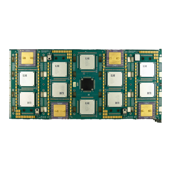
1.1 System Components and Features Figure 1–2 Board Component Layout 33.15 cm (13.05 in) 30.73 cm (12.10 in) MK−2306−32 1.2 EB164 Summary The features of the EB164 are listed and described in Table 1–2. 1–6 Introduction to the EB164... -
Page 15: Eb164 Features Summary
Digital sales representative. System Characteristics CPU and clock speed Digital Semiconductor 21164 Alpha microprocessor at 266, 300, or 333 MHz CPU upgradable ZIF socket for 21164 upgrade Instruction issue Up to 4 instructions issued per clock cycle... - Page 16 1.2 EB164 Summary Table 1–2 (Cont.) EB164 Features Summary Characteristic Description Input/Output Input device interfaces PS/2 style keyboard and mouse Serial Two RS423-compatible (9-position) serial communications ports Parallel One parallel (Centronics compatible) communications port Bus options Total of 6 option slots PCI bus Supports two 64-bit PCI options slots at 5V and two 32-bit PCI option slots at 5V...
-
Page 17: System Configuration And Connectors
System Configuration and Connectors The EB164 uses jumpers to implement configuration parameters such as variations in backup cache (Bcache) size, access timing, and speed, as well as boot parameters. These jumpers must be configured for the user’s environment. Onboard connectors are provided for the I/O interfaces, single inline memory modules (SIMMs), and serial and parallel peripheral ports. -
Page 18: Eb164 Jumper Locations
2.1 Configuration Jumpers Figure 2–1 EB164 Jumper Locations MK−2306−30 2–2 System Configuration and Connectors... -
Page 19: Configuration Jumpers
2.1 Configuration Jumpers Figure 2–2 Configuration Jumpers irq3 irq2 index22 irq1 irq0 Reserved CONF4 index21 BC_SIZE<2> BC_SIZE<1> CONF5 CONF6 BC_SIZE<0> CONF7 BC_SPEED<2> index20 CONF8 BC_SPEED<1> CONF9 BC_SPEED<0> CONF10 Mini−Debugger BOOT_OPTION CONF11 Flash ROM Write Protect/ CONF12 Reserved Write Enable CONF13 BC_RD_FAST CONF14 Reserved... -
Page 20: Configuration Jumper Position Descriptions
2.1 Configuration Jumpers Table 2–1 Configuration Jumper Position Descriptions Feature Jack/Jumper—Pins and Description System clock J1—1/2, —3/4, —5/6, —7/8 divisor J1—1/2 J1—3/4 J1—5/6 J1—7/8 (irq3) (irq2) (irq1) (irq0) Ratio Divisor 8 is used for 266 MHz. Divisor 9 is used for 300 MHz. Divisor 10 is used for 333 MHz. - Page 21 2.1 Configuration Jumpers Table 2–1 (Cont.) Configuration Jumper Position Descriptions Feature Jack/Jumper—Pins and Description BC_SIZE<2:0> J1—11/12 (CONF4), —13/14 (CONF5), —15/16 (CONF6) These jumpers allow the Bcache to emulate the sizes specified in the following table. These jumpers are changed in conjunction with the appropriate index jumpers J17, J16, and J15.
- Page 22 2.1 Configuration Jumpers Table 2–1 (Cont.) Configuration Jumper Position Descriptions Feature Jack/Jumper—Pins and Description BC_SPEED<2:0> J1—17/18 (CONF7), —19/20 (CONF8), —21/22 (CONF9) These jumpers select the Bcache timing parameters used to compute the BC_CONFIG register value. Select the jumper configuration that matches the access time for the SRAMs being used.
- Page 23 2.1 Configuration Jumpers Table 2–1 (Cont.) Configuration Jumper Position Descriptions Feature Jack/Jumper—Pins and Description BOOT_OPTION J1—25/26 (CONF11) This jumper selects the image to be loaded into memory from the system flash ROM. With the jumper out (bit = 1), the first image (debug monitor) is loaded.
-
Page 24: Eb164 Connectors
2.2 EB164 Connectors 2.2 EB164 Connectors Figure 2–3 shows the EB164 connectors and Table 2–2 describes them. Figure 2–4 provides a detail of header connector J2. Figure 2–3 EB164 Connector Locations MK−2306−31 2–8 System Configuration and Connectors... -
Page 25: Detail Of Header Connector J2
2.2 EB164 Connectors Figure 2–4 Detail of Header Connector J2 Ground Pins: 5, 8, 9, 12, 13, 16, 18, 22, and 25 Fan 1 +12−V Pins: 3, 7, and 11 Fan 2 System Halt Button Fan 3 System Reset Button IDE Drive Active Indicator... -
Page 26: Eb164 Connector Descriptions
2.2 EB164 Connectors Table 2–2 EB164 Connector Descriptions Connector Pins Description Main Memory/Bcache SIMMs DRAM 0 SIMM DRAM 1 SIMM DRAM 2 SIMM DRAM 3 SIMM DRAM 4 SIMM DRAM 5 SIMM DRAM 6 SIMM DRAM 7 SIMM Note: To fill a 256-bit data path, all SIMM connectors J3 through J10 must be populated. - Page 27 2.2 EB164 Connectors Table 2–2 (Cont.) EB164 Connector Descriptions Connector Pins Description Mouse Connector Mouse connector National 87312 Combination Chip Connectors Parallel port connector Connects to an external 25-pin connector. Serial communication port 1 connector Note: This connector can be used as a terminal port for the debug monitor.
- Page 28 2.2 EB164 Connectors Table 2–2 (Cont.) EB164 Connector Descriptions Connector Pins Description Speaker J2—19/21/23/25 — Speaker connector pins Power On Indicator J2—26 Power on indicator pin Connect LED from this pin to ground. System Halt Button J2—8/10 System halt button pins System Reset Button J2–12/14 System reset button pins...
- Page 29 2.2 EB164 Connectors Table 2–2 (Cont.) EB164 Connector Descriptions Connector Pins Description Power Connectors Board power connector Voltage/Signal +3.3 V +3.3 V +3.3 V Ground Ground Ground Ground Ground Ground +3.3 V +3.3 V +3.3 V (continued on next page) System Configuration and Connectors 2–13...
- Page 30 2.2 EB164 Connectors Table 2–2 (Cont.) EB164 Connector Descriptions Connector Pins Description Board power connector Voltage/Signal p_dcok Vdd (+5 V) +12 V –12 V Ground Ground Ground Ground –5 V Vdd (+5 V) Vdd (+5 V) Vdd (+5 V) Note: Power for the EB164 is provided by a user-supplied power supply.
-
Page 31: Starting And Using The Eb164
Starting and Using the EB164 This chapter lists hardware, software, and accessories that users must obtain to completely furnish a functioning computer system. The chapter then describes how to configure the hardware and software. Finally, the chapter describes how to start and use the EB164. 3.1 Hardware Requirements Before turning on the power to your EB164, you must provide the following components in addition to those supplied in the kit. -
Page 32: Software Requirements
3.1 Hardware Requirements • A 3.5-in diskette drive and cable. • A 9-pin serial line cable. • A terminal or a serial line connection to a host system with appropriate cables. Refer to the Alpha Microprocessors Evaluation Board Windows NT 3.51 Installation Guide provided in the EB164 Windows NT 3.51 Installation Kit and the Hardware Compatibility List for Windows NT to determine which SCSI controllers and graphics cards are supported. - Page 33 3.3 Hardware Configuration 1. Install the 21164 Alpha microprocessor in ZIF socket U42. a. Observe antistatic precautions. b. Lift the ZIF socket actuator handle to a full 90° angle. Make sure that all the pins on the 21164 are straight. d.
-
Page 34: Fan/Heat Sink Assembly
3.3 Hardware Configuration Refer to Figure 3–1 for heat sink and fan assembly details. Figure 3–1 Fan/Heat Sink Assembly Screw, 6-32 x 0.875 in Qty 4 Guard, Fan Clip, Heat Sink/Chip/Fan Nut, Hex, 1/4-20, 2011-T3 Aluminum, 0.438 in Across Flats, Qty 2 Torque to 20 +/- 2 in-lbs Heat Sink, with Fan Mounting Holes... - Page 35 3.3 Hardware Configuration 2) Wearing clean gloves, pick up the GRAFOIL pad. Do not do this with bare hands because skin oils can be transferred to the pad. 3) Place the GRAFOIL pad on the gold-plated slug surface and align it with the threaded studs.
- Page 36 3.3 Hardware Configuration 4. Install the two L3 cache SRAM SIMMs into sockets J11 and J12. Refer to Table 2–2 for socket locations. 5. Install eight system memory DRAM SIMMs. Refer to Table 2–2 for socket locations. a. Observe antistatic precautions. Handle SIMMs at the edges only to prevent damage.
-
Page 37: Eb164 Power Connectors
3.3 Hardware Configuration Figure 3–2 EB164 Power Connectors Voltage/Signal EB164 Board p_dcok (+5 V) +12 V −12 V Ground Ground Ground Ground −5 V (+5 V) (+5 V) (+5 V) 21164 Microprocessor Voltage/Signal +3.3 V +3.3 V +3.3 V Ground Ground Ground Ground... -
Page 38: Software Configuration
3.3 Hardware Configuration 11. If you will be using an IDE hard drive, attach your IDE cable to connector J28 in the proper orientation and install your hard drive. The disk should be configured as the primary device on the IDE bus. Refer to the manufacturer’s instructions for setting up the hard drive. -
Page 39: Starting Windows Nt Arc Firmware
3.4 Software Configuration 3.4.1 Starting Windows NT ARC Firmware Start the Windows NT ARC firmware using the following procedure. 1. Verify that the jumper from J14-2 to J14-3 is inserted, allowing the flash ROM to be written. If the Windows NT ARC firmware is unable to write to flash ROM, it prints the message and stops. -
Page 40: Returning To Windows Nt Arc Firmware From The Debug Monitor
3.4 Software Configuration 3.4.3 Returning to Windows NT ARC Firmware from the Debug Monitor The following methods may be used to return to the Windows NT ARC firmware from the debug monitor. A. If you used item A in section Section 3.4.2 to enter the debug monitor, then use this procedure to return to Windows NT ARC firmware. - Page 41 3.4 Software Configuration B. If you used item B in section Section 3.4.2 to enter the debug monitor, then use this procedure to return to Windows NT ARC firmware. 1. Turn off the power to the EB164, insert the jumper from J1-25/26 (CONF11 on the module).
-
Page 43: Functional Description
Functional Description This chapter describes the functional operation of the EB164. The description introduces the Digital Semiconductor 21171 ASIC support chipset and describes its implementation with the 21164 microprocessor, its supporting memory, and I/O devices. Figure 1–1 shows the EB164 major functional components. -
Page 44: Interrupt Logic
4.1 PCI Interrupts and Arbitration Figure 4–1 Interrupt Logic 4–2 Functional Description... -
Page 45: Eb164 System Interrupts
4.1 PCI Interrupts and Arbitration The PCI-to-ISA SIO bridge chip provides the functionality of two 8259 interrupt control devices. These ISA-compatible interrupt controllers are cascaded such that 14 external and two internal interrupts are available. The PCI interrupt acknowledge command should be used to read the interrupt request vector from the SIO. -
Page 46: Pci-To-Isa Sio Bridge Interrupts
4.1 PCI Interrupts and Arbitration Table 4–2 PCI-to-ISA SIO Bridge Interrupts Priority Label Controller Internal/External Interrupt Source IRQ0 Internal Internal timer 1 IRQ1 External Keyboard 3–10 IRQ2 Internal Interrupt from controller 2 IRQ8# External Reserved IRQ9 External ISA bus pin B04 IRQ10 External ISA bus pin D03... -
Page 47: Arbitration
4.1 PCI Interrupts and Arbitration Figure 4–2 Interrupt and Interrupt Mask Registers Interrupt and Interrupt Mask Register 1 (ISA Address 804h) intb2 intb1 intb0 inta3 inta2 inta1 inta0 Interrupt and Interrupt Mask Register 2 (ISA Address 805h) intd2 intd1 intd0 intc3 intc2 intc1... -
Page 48: Dc Power Distribution
4.3 dc Power Distribution Figure 4–3 dc Power Distribution 4–6 Functional Description... -
Page 49: Pci Devices
4.3 dc Power Distribution As shown in Figure 4–3, the +12 V dc, –12 V dc, and –5 V dc are supplied to ISA connectors J19, J20, and J21. The +12 V dc and –12 V dc are supplied to ISA connectors and PCI32 connectors J24 and J25. The +12 V dc is also supplied to the CPU fan connector J30, auxiliary fan connector pins on header J2, and to the flash ROM write-enable conector J14. -
Page 50: Flash Rom
4.5 Flash ROM 4.5 Flash ROM The flash ROM, sometimes called the system ROM, is a 1MB, nonvolatile, writable ROM. After the serial ROM (SROM) code initializes the EB164 system, the flash ROM code prepares the system for booting. The flash ROM headers, structure, and access methods are described here. -
Page 51: Special Header Entry Descriptions
4.5 Flash ROM Table 4–3 describes each entry in the special header. Table 4–3 Special Header Entry Descriptions Entry Description Validation and inverse This quadword contains a special signature pattern used to validation pattern validate that the special ROM header has been located. The pattern is 5A5AC3C3A5A53C3C. - Page 52 4.5 Flash ROM Table 4–3 (Cont.) Special Header Entry Descriptions Entry Description Header revision The revision of the header specification used in this header. This is necessary to provide for changes to the header specification. Version 0 headers are identified by the size of the header (32 bytes).
-
Page 53: Flash Rom Structure
4.5 Flash ROM 4.5.2 Flash ROM Structure During the power-up and initialization sequence, the EB164 always loads the first image if BOOT_OPTION=1 (jumper J1—25/26 not installed). Then the first image (the debug monitor) will be booted. If jumper J1—25/26 (BOOT_OPTION) is installed (see Figure 2–2), the EB164 reads the value at location 0x3F of the TOY RAM. - Page 54 4.5 Flash ROM Changing TOY RAM Location 0x3F—Debug Monitor Command bootopt Use the debug monitor command to change the value in location 3F. bootopt In the example shown here, the command is used to change the value bootopt in location 3F from 0 to 1: EB164>...
-
Page 55: Flash Rom Access
4.5 Flash ROM 4.5.3 Flash ROM Access The flash ROM can be viewed as two banks of 512KB each. At power-up the lower 512KB bank is accessed using the address range 86.FFF8.0000 to 86.FFFF.FFFF. Setting address bit 19 (flash_adr19) allows you to access the higher 512KB of flash ROM. -
Page 57: Eb164 Requirements, Power, And Parameters
EB164 Requirements, Power, and Parameters This chapter describes the EB164 environmental requirements, power, and physical board parameters. 5.1 Power Requirements The EB164 derives its main dc power from a user-supplied power supply. The board has a total power dissipation of 116 W, excluding any plug-in PCI and ISA devices. -
Page 58: Environmental Requirements
5.2 Environmental Requirements 5.2 Environmental Requirements The 21164 microprocessor is cooled by a small fan blowing directly into the chip’s heat sink. The EB164 motherboard is designed to run efficiently using only this fan. Additional fans may be necessary depending upon cabinetry and I/O board requirements. - Page 59 5.3 Physical Board Parameters Figure 5–1 Board Component Layout 33.15 cm (13.05 in) 30.73 cm (12.10 in) MK−2306−32 EB164 Requirements, Power, and Parameters 5–3...
-
Page 60: Board Component List
Table 5–2 Board Component List Locator Component Number Number Component Description Digital Semiconductor 21164 Alpha microprocessor 21171-CA control, I/O interface, and address (CIA) chip 21171-BA data switch (DSW0) chip 21171-BA data switch (DSW2) chip 21171-BA data switch (DSW1) chip 21171-BA data switch (DSW3) chip TriQuint TQ2061 phase-locked loop (PLL) clock chip 26.66-MHz clock oscillator... -
Page 61: A Supporting Vendor Products
Supporting Vendor Products To obtain components and accessories that are not included with your EB164 motherboard, Digital Equipment Corporation suggests the following vendors. In doing so, Digital does not warrant these components or guarantee that they will function in all configurations. -
Page 62: Products Not Included
A.1 Products Included • Bcache (Level 3) cache SIMMs SIMM Cache Size Configuration Qty Vendor/Part Number 2MB @10 ns 128K Digital PN, 21A04-M1 A.2 Products Not Included The following products are not included in the EB164 motherboard kit. • DRAM system memory—70 ns DRAM SIMMs (5 V, 72 pin) 36, 2M 36, 4M 36, 8M... -
Page 63: B Technical Support And Ordering Information
The following table lists some of the semiconductor products available from Digital. To obtain a Digital Semiconductor Product Catalog, contact the Digital Semiconductor Information Line. Product Order Number Digital Semiconductor 21164 Alpha Microprocessor Motherboard 21A04-A0 (EB164) 266-MHz Kit (Supports the Windows NT operating system.) Digital Semiconductor 21164 333-MHz Alpha Microprocessor 21164–333... -
Page 64: Ordering Digital Semiconductor Literature
Alpha 21164 Microprocessor Evaluation Board Read Me EC–QD2VB–TE First Alpha 21164 Microprocessor Evaluation Board Product EC–QCZZD–TE Brief Digital Semiconductor 21164 Alpha Microprocessor EC–QD2UD–TE Evaluation Board User’s Guide DECchip 21171 Core Logic Chipset Product Brief EC–QC3EB–TE DECchip 21171 Core Logic Chipset Technical Reference EC–QE18B–TE... -
Page 65: Ordering Third-Party Literature
B.4 Ordering Third-Party Literature B.4 Ordering Third-Party Literature You can order the following third-party literature directly from the vendor: Title Vendor PCI System Design Guide PCI Special Interest Group 1–800–433–5177 (U.S.) 1–503–797–4207 (International) 1–503–234–6762 (FAX) PCI Local Bus Specification, Rev 2.1 PCI Special Interest Group (See previous entry.) 82420/82430 PCIset ISA and EISA... -
Page 67: Index
Index Airflow requirements, 5–2 Cache Alpha See Bcache documentation, B–2 21171 chipset, 1–1 Arbitration scheme, 4–5 Chipset support, 1–1 Associated literature, B–2 Clock divisor jumper, 2–4 COM1 connector, 2–11 COM2 connector, 2–11 Components Backup cache See System components See Bcache Configuration, 2–1 to 2–14 Bcache hardware, 3–2... - Page 68 Conventions, viii Flash ROM, 1–5 Cooling fan, CPU developing code, 1–4 power connectors, 2–14 loading code, 1–4 sensor connector, 2–14 write-enable jumper, 2–7 Current write-protect jumper, 2–7 dc ampere requirements, 5–1 Floppy drive See Diskette drive Functional description, 4–1 to 4–13 dc power distribution, 4–5 to 4–7 dc power distribution, 4–5 interrupts, 4–1 to 4–4...
- Page 69 ISA (cont’d) devices, 4–5 interface overview, 1–4 Operating systems flash ROM support, 1–4 software support, 1–5 Jumpers, 2–1 supported operating systems, 1–7 Bcache index, 2–5 Ordering products, B–1 Bcache size, 2–4 Bcache speed, 2–5 BC_RD_FAST, 2–7 boot option, 2–6 Parallel port connector, 2–11 Flash ROM write-protect/write-enable, Parts 2–7...
- Page 70 System I/O chip See SIO chip System ROM Saturn I/O chip See Flash ROM See SIO chip System software Semiconductor Information Line, B–1 software support, 1–5 Serial interface connectors, 2–11 Serial ROM See SROM SIMM Technical support, B–1 connectors, 2–10 Third-party documentation, B–3 Single inline memory module Tools, 3–3...
Need help?
Do you have a question about the Digital Semiconductor 21164 Alpha Microprocessor and is the answer not in the manual?
Questions and answers