Table of Contents
Advertisement
Quick Links
APPLICATION
NEXT ASSY
FINAL ASSY
REV
C
C
C
SHEET
1
2
3
PROJ. NO.
411
NOTICE IS HEREBY GIVEN THAT THIS DRAWING IS PART
OF A PROPRIETARY ITEM OWNED BY INDUSTRIAL
ELECTRONIC ENGINEERS, INC. AND SHALL NOT BE
REPRODUCED, OR COPIED OR USED AS THE BASIS FOR
MANUFACTURE OR SALE OF APPARATUS WITHOUT
WRITTEN PERMISSION OF I.E.E. INC.
LTR
–
PRODUCTION RELEASE/E.O. 29226
A
E.O. 29434
B
E.O. 29653
C
E.O. 36743, Revised and Redrawn
4 x 20 Daystar Nova LCD Module
C
C
C
C
C
C
4
5
6
7
8
9
CONTRACT
R. January
DRAWN
CHECK
APPROVED
D. Goodale 3-19-93
APPROVED
DESCRIPTION
Specification
With
Parallel Data Input Option
Model 03805–06–0100
C
C
C
C
C
10
11
12
13
14
REVISION STATUS
3–19–93
SIZE
CODE IDENT NO.
05464
A
SCALE
REVISIONS
11/30/93
C
C
C
C
C
15
16
17
18
19
INDUSTRIAL ELECTRONIC ENGINEERS, INC.
VAN NUYS, CALIFORNIA
PARALLEL DATA INPUT
4 X 20 LCD MODULE
S03805–06–0100
SHEET
DATE
APPROVED
3/19/93
D. Goodale
6/3/93
D. Goodale
D. Goodale
2/12/02
D. Goodale
C
20
21
22
23
24
1
OF
20
Advertisement
Table of Contents

Related Manuals for IEE 03805-06-0100


Summary of Contents for IEE 03805-06-0100
- Page 1 APPLICATION REVISIONS NEXT ASSY FINAL ASSY DESCRIPTION DATE APPROVED – PRODUCTION RELEASE/E.O. 29226 3/19/93 D. Goodale E.O. 29434 6/3/93 D. Goodale E.O. 29653 11/30/93 D. Goodale E.O. 36743, Revised and Redrawn 2/12/02 D. Goodale Specification 4 x 20 Daystar Nova LCD Module With Parallel Data Input Option Model 03805–06–0100...
-
Page 2: Table Of Contents
Table of Contents Paragraph Title Page GENERAL INFORMATION..........................4 1.1 Introduction..............................4 1.2 Application ..............................4 1.3 Description ..............................4 LOGICAL STRUCTURE AND FUNCTION ....................5 2.1 Module Block Diagram ..........................5 2.1.1 Signal Description..........................5 2.2 LCD Controller ..............................6 2.2.1 Instruction Register (IR).........................6 2.2.2 Data Register (DR)..........................6 2.2.3 Busy Flag ...............................6 2.2.4 Address Counter (AC) ...........................6 2.2.5 Display Data RAM (DD RAM) ........................7... - Page 3 List of Figures Figure Title Page Figure 1 Module Block Diagram ...........................5 Figure 2 LCD Controller Block Diagram ......................6 Figure 3 Correspondence Between Character Codes and Character Patterns ..........7 Figure 4 Relationship Between CG RAM Address, Character Codes (DD RAM) and Character Patterns (CG RAM Data)............................8 Figure 5 LCD Controller Instruction Set.......................9...
-
Page 4: General Information
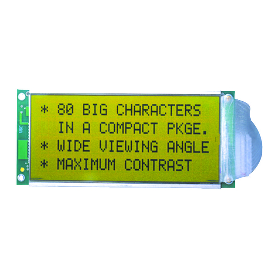
Super Bi–refringent Effect (SBE) liquid crystal cell used in this display. For applications where the display is remotely located up to 50 feet from the host processor, the serial data input option should be used. The serial option model is described in IEE specification S03805–06–0200. Description The Daystar Nova module is a self–contained 1/16 multiplexed unit. -
Page 5: Logical Structure And Function
LOGICAL STRUCTURE AND FUNCTION Module Block Diagram Figure 1 illustrates the major components of the Daystar Nova module. The microprocessor controls all multiplexing and character decoding. The temperature compensation network optimizes both viewing and contrast ratio for the display over all operating temperatures. LCD Display LCD Row Drivers and LCD Column Drivers... -
Page 6: Lcd Controller
LCD Controller Address Timing Generation Counter (AC) Circuit Display Data (DD RAM) Com1–Com16 80x8 bits DB4–DB7 DB0–DB3 Character Character Generator Generator (CG RAM) (CG ROM) Busy Seg1–Seg40 Flag 512 Bits 7200 Bits Parallel/Serial Data Conversion Circuit 40–bit Shift Register (Parallel Data –Serial Data) Figure 2 LCD Controller Block Diagram 2.2.1 Instruction Register (IR) -
Page 7: Display Data Ram (Dd Ram)
address and position of the characters in the display can be controlled by the user (Refer to Entry Mode Set and Cursor or Display Shift instructions). 2.2.6 Character Generator ROM (CG ROM) The CG ROM generates character patterns of 5 X 7 dots from 8 bit character codes. The 192 5 X 7 dot matrix characters are illustrated in Figure 3. -
Page 8: Character Generator Ram (Cg Ram)
between CG RAM addresses and data patterns (Refer to Set CG RAM Address and Write to CG or DD RAM instructions). Character Codes CG RAM Character Patterns (DD RAM Data) Address (CG RAM Data) Higher Order Bits Higher Order Bits Higher Order Bits Lower Order Bits Lower Order Bits... -
Page 9: Operation
OPERATION Instruction Set Instruction Code Description Execution R/W DB Time (Max) Clear Display Clears entire display and sets DD RAM to 0 1.64 ms Sets DD RAN counter to 0. If the display has been shifted, characters are returned to their initial Return Home 1.64 ms positions. -
Page 10: Power Up Instructions Sequence
Power Up Instructions Sequence Upon power up, the Daystar Nova module is set to a default mode of operation. Under some power up circumstances, the default mode may be improperly set. Consequently, the following instructions should always be executed in the host systems initialization routine. Step Operation Function Set for 8 bits... -
Page 11: Instructions Affecting Custom Characters
* = Cursor Figure 8 Display Shift Right from Initial Conditions * = Cursor # = Last Character Entered Figure 9 Load Character with S=1, I/D=0 from Initial Conditions * = Cursor # = Last Character Entered Figure 10 Load Character with S=1, I/D=1 from Initial Conditions Instructions Affecting Custom Characters The module allows the user to define 8 unique special characters. -
Page 12: Electrical Characteristics
Electrical Characteristics (V = 5V ±10%) Item Symbol Condition Unit Input "High" Voltage Input "Low" Voltage –0.3 Output "High" Voltage (TTL) = 0.205 mA – Output "Low" Voltage (TTL) = 1.200 mA – Output "High" Voltage (CMOS) = 0.040 mA 0.9 V –... -
Page 13: Figure 11 Interface Timing (Write)
t t t t t t t t t t t t – DB Valid Data Figure 11 Interface Timing (Write) – DB Valid Data Figure 12 Interface Timing (Read) SIZE CODE IDENT Industrial Electronic Engineers, Inc. S03805–06–0100 05464 Van Nuys, California Scale: NONE Rev C Sheet 13... -
Page 14: Timing Sequence For 8 Bit Parallel Interface
Timing Sequence for 8 Bit Parallel Interface Figure 13 illustrates the typical Busy Flag check sequence for an 8 bit data interface. Internal Internal Operation Data Busy Busy IR 7 Busy Instruction Busy Flag Busy Flag Busy Flag Instruction Write Check Check Check... -
Page 15: Connector Pin Assignments (P1)
Connector Pin Assignments (P1) Pin No. Function (Factory Set–up Test Point) BIAS N/C * (Viewing Angle Adjustment) (Read = Logic 1) (Pin Removed) Ground Enable (E1) Ground Ground Ground Ground Ground Ground (+5V – Parallel with Pin 24) (+5V – Parallel with Pin 22) When the display module includes the serial data input option, Pin 3 is internally connected to provide signal E2 as an output to a second display module. -
Page 16: Environmental Characteristics
ENVIRONMENTAL CHARACTERISTICS Operating Temperature: –30 to +80°C Humidity: (@ 40ºC) 95% RH (non–condensing) Humidity ( 40 C): Absolute humidity must be lower the humidity of 95% RH at 40 C Vibration: 10g at 10 to 400Hz (3 axes) Shock: 10g (all axes) Non–Operating Temperature: –40°C to +85°C... -
Page 17: Viewing Angle Adjustment
Normal = +90º –X = –90º –Y Figure 15 Definition of Vertical Viewing Angle Definition of Horizontal Viewing Angle–top Viewing Display (for Bottom Viewing Displays = –20° Typically) Normal = +20º – –X = –90º = +90º –Y Figure 16 Definition of Horizontal Viewing Angle Display contrast ratio is given by: Where: B... - Page 18 Brightness Curve for Selected Segment Brightness Curve for Non–selected Segment Setpoint Driving Voltage Figure 17 Definition of Contrast Ratio (CR) Definition of optical response. 10% ON 90% ON Excitation Figure 18 Definition of Optical Response Viewing Angle Adjustment The factory preadjusts the viewing angle of the display by setting the LCD bias voltage to 10.2 Volts using the on–board potentiometer.
-
Page 19: Installation Note
INSTALLATION NOTE To protect the front polarizer from accidental damage it is highly recommended that the LCD be mounted behind a clear glass or polycarbonate window material. It is also recommended that an air gap of at least .030" to .050" minimum be provided between the window material and the surface of the LCD to prevent the transfer of static charges to the front surface of the LCD. -
Page 20: Van Nuys, California Scale: None Rev C Sheet
OUTLINE AND INSTALLATION CHARACTERISTICS Figure 19 03805–06–0100 Outline Drawing SIZE CODE IDENT Industrial Electronic Engineers, Inc. S03805–06–0100 05464 Van Nuys, California Scale: NONE Rev C Sheet 20...
Need help?
Do you have a question about the 03805-06-0100 and is the answer not in the manual?
Questions and answers