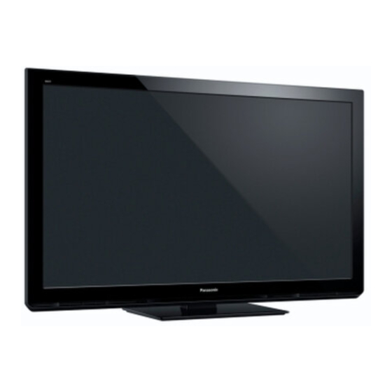
Summarization of Contents
Safety Precautions
General Guidelines
General guidelines for conducting repairs and servicing equipment.
Touch-Current Check
Procedure for checking leakage current to prevent shock hazards.
Warning
Prevention of Electrostatic Discharge (ESD) to Electrostatically Sensitive (ES) Devices
Techniques to reduce component damage from static electricity.
About Lead Free Solder (PbF)
Information and recommendations for using lead-free solder.
Service Navigation
PCB Layout
Identifies main circuit boards and their locations within the unit.
Applicable Signals
Lists compatible video signals for Component and HDMI inputs.
Technical Descriptions
Specification of KEY for CI Plus, DTCP-IP and One-to-One
Details about KEY data generation and IC replacement for specific features.
Service Mode
How to Enter into Service Mode
Procedure to access and navigate the service menu.
Contents of Adjustment Mode
Lists adjustable parameters within the service mode.
Option - Mirror
How to reverse picture orientation (left/right, up/down).
Service Tool Mode
How to access and use the service tool mode.
Data Copy by SD Card
Data Copy from TV Set to SD Card
Step-by-step guide for copying TV data to an SD card.
Data Copy from SD Card to TV Set
Step-by-step guide for copying data from an SD card to the TV.
Troubleshooting Guide
Check of the IIC Bus Lines
How to access and perform IIC bus line checks.
Power LED Blinking Timing Chart
Identifies defective blocks based on power LED blink patterns.
No Power
Troubleshooting steps for when the unit does not power on.
No Picture
Troubleshooting flowchart for issues related to no picture.
Disassembly and Assembly Instructions
Remove the Rear Cover
Steps to remove the rear cover of the unit.
Remove the AC Inlet
Steps to safely remove the AC inlet.
Remove the P-Board
Steps to remove the Power Supply board (P-Board).
Remove the Side Terminal Cover
Steps to remove the side terminal cover.
Component Removal
Remove the Tuner Unit
Steps to remove the tuner unit.
Remove the A-Board
Steps to remove the Main AV input board (A-Board).
Remove the SN-Board
Steps to remove the Scan Drive board (SN-Board).
Remove the SS-Board
Steps to remove the Sustain Drive board (SS-Board).
Further Disassembly
Remove the Stand Bracket and the Hanger Metals
Steps to remove the stand bracket and hanger metals.
Remove the C1-Board
Steps to remove the C1-Board (Data Driver Lower Right).
Remove the C2-Board
Steps to remove the C2-Board (Data Driver Lower Left).
Panel and Board Removal
Remove the Plasma Panel Section from the Cabinet Assy
Steps to remove the plasma panel section from the cabinet assembly.
Remove the K-Board
Steps to remove the K-Board (Remote receiver, Power LED).
Plasma Panel Replacement
Replace the Plasma Panel
Caution and procedure for replacing the plasma panel.
Measurements and Adjustments
Adjustment
General information on performing adjustments.
Vsus Selection
Procedure to set the Vsus level (LOW or HIGH).
Sub-Contrast Adjustment
Steps for adjusting sub-contrast for RF, AV, and HD systems.
White Balance Adjustment
Method for adjusting white balance based on EEPROM version.
Block Diagram
Main Block Diagram
Overall block diagram of the TV's main functional units.
Block (1/4) Diagram
Detailed block diagram of the Main AV Input Processing section.
Block (2/4) Diagram
Detailed block diagram of the Plasma AI, C.A.T.S. Sensor, and other components.
Block (3/4) Diagram
Detailed block diagram of the Power Supply unit.
Block (4/4) Diagram
Detailed block diagram of the Scan Drive and Data Driver sections.
Wiring Connection Diagram
Caution Statement
General caution regarding flexible cable connections.
Wiring (1)
Shows the connection of the P9 connector and AC inlet.
Wiring (2)
Wiring diagram showing connections between various boards (SN, P, P, C, SS).
Wiring (3)
Wiring diagram showing connections between SN, A, P, and A boards.
Wiring (4)
Wiring diagram illustrating wire routing and clamp usage.


Need help?
Do you have a question about the TX-P50C3J and is the answer not in the manual?
Questions and answers