Table of Contents
Advertisement
Quick Links
Advertisement
Table of Contents

Related Manuals for Clevo W955BU


Summarization of Contents
Preface
Notice
Company reserves the right to revise publication content and change specifications without notice.
Trademarks
Lists registered trademarks like Intel Corporation's Pentium and Celeron, and Microsoft's Windows.
About this Manual
Manual intended for service personnel, covering servicing and upgrading notebook components.
IMPORTANT SAFETY INSTRUCTIONS
Basic safety precautions to reduce risks of fire, electric shock, and injury when using equipment.
Instructions for Care and Operation
Suggestions for proper care and operation to prevent damage to the notebook.
Power Safety
Details specific power requirements and warnings for using the computer and its adapter.
Battery Precautions
Precautions regarding battery usage, handling, and disposal to avoid damage or fire.
Related Documents
Lists other manuals for additional information on the notebook PC.
System Startup
Step-by-step instructions for setting up and starting the notebook computer.
Chapter 1: Introduction
Overview
Introduces the manual's scope, covering service and upgrade information for the W950BU/W955BU series notebook.
Specifications
Details the technical specifications of the notebook, including processor, audio, storage, and more.
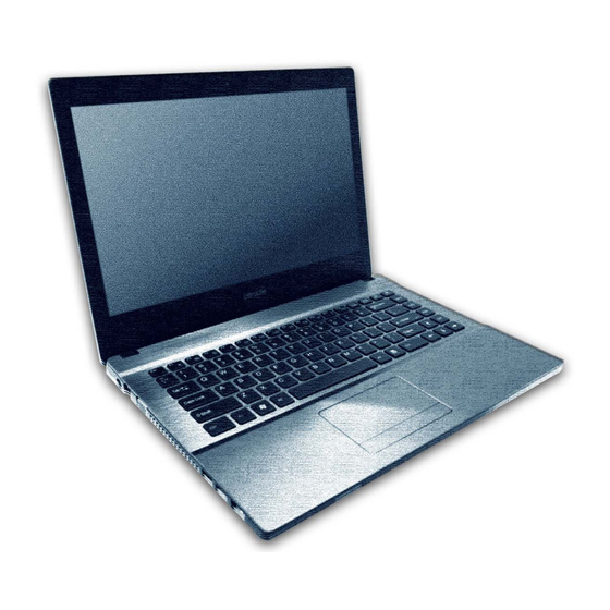
External Locator - Top View with LCD Panel Open
Identifies external components on the top view of the notebook with the LCD open.
External Locator - Front & Right Side Views
Identifies external components on the front and right side views of the notebook.
External Locator - Left Side & Rear View
Identifies external components on the left side and rear views of the notebook.
External Locator - Bottom View
Identifies external components on the bottom view of the notebook, including vents and speakers.
Mainboard Overview - Top (Key Parts)
Illustrates the top side of the mainboard and identifies key components.
Mainboard Overview - Bottom (Key Parts)
Illustrates the bottom side of the mainboard and identifies key components.
Mainboard Overview - Top (Connectors)
Shows the top side of the mainboard and labels various connectors.
Mainboard Overview - Bottom (Connectors)
Shows the bottom side of the mainboard and labels various connectors.
Chapter 2: Disassembly
Overview
Introduces the disassembly chapter, providing guidance on procedures and safety.
Maintenance Tools
Lists the recommended tools for performing maintenance on the notebook PC.
Maintenance Precautions
Lists precautions to avoid personal injury or damage during maintenance and replacement.
Disassembly Steps
A table detailing disassembly steps for components and corresponding page numbers for detailed instructions.
Removing the Battery
Step-by-step instructions with figures for safely removing the notebook's battery.
Removing the Hard Disk Drive
Provides instructions for removing and upgrading the hard disk drive.
Removing the Optical (CD/DVD) Device
Step-by-step guide with figures on how to remove the optical drive.
Removing the Caddy/Second Hard disk
Instructions for removing the caddy and the second hard disk drive.
Removing the System Memory (RAM)
Detailed steps for removing and replacing the system memory modules (RAM).
Removing the M.2 SSD Module
Instructions for removing the M.2 Solid State Drive module from the notebook.
Removing the Keyboard
Step-by-step guide on how to remove and replace the keyboard.
Removing the 3G Module
Instructions for removing the 3G module, including disconnecting cables and screws.
Removing the Wireless LAN Module
Steps to remove the Wireless LAN module, including cable and screw disconnection.
Wireless LAN and Combo Module Cables
Information on identifying WLAN and Bluetooth combo module cables by color and type.
Removing the CCD
Instructions for removing the CCD module, involving LCD panel disassembly.
Appendix A: Part Lists
Part List Illustration Location
A table directing users to specific pages for part list illustrations of various notebook components.
Top - W950BU
Part list illustration for the top assembly of the W950BU model.
Top - W955BU
Part list illustration for the top assembly of the W955BU model.
Bottom (W950BU)
Part list illustration for the bottom assembly of the W950BU model.
Bottom (W955BU)
Part list illustration for the bottom assembly of the W955BU model.
LCD (W950BU)
Part list illustration for the LCD assembly of the W950BU model.
LCD (W955BU)
Part list illustration for the LCD assembly of the W955BU model.
DVD DUAL (W950BU)
Part list illustration for the DVD dual drive of the W950BU model.
DVD DUAL (W955BU)
Part list illustration for the DVD dual drive of the W955BU model.
Dummy ODD (W950BU)
Part list illustration for the dummy ODD of the W950BU model.
HDD (W950BU)
Part list illustration for the HDD of the W950BU model.
HDD (W955BU)
Part list illustration for the HDD of the W955BU model.
2nd HDD (W950BU)
Part list illustration for the 2nd HDD of the W950BU model.
Appendix B: Schematic Diagrams
SCHEMATIC DIAGRAMS
A table listing diagrams available in this appendix and their corresponding page numbers.
System Block Diagram
Provides a high-level overview of the system's architecture and component interconnections.
Skylake ULT DDR
Schematic diagram illustrating the DDR memory interface and connections for the Skylake ULT platform.
Skylake ULT RTC/HDA/CLK/SD
Schematic diagram for Real-Time Clock, High Definition Audio, Clock, and SD card interfaces.
Skylake ULT LPC/SPI/SMB
Schematic diagram detailing the LPC, SPI, and SMBus interfaces for the Skylake ULT platform.
Skylake ULT Power Maint
Schematic diagram illustrating power management and maintenance signals for the Skylake ULT.
Skylake ULT GPIOS/I2C/EMMC
Schematic diagram for General Purpose I/O, I2C, and EMMC interfaces.
Skylake ULT PCIE, USB, SATA
Schematic diagram showing PCIe, USB 3.0, and SATA interfaces.
Skylake ULT Power 1
Schematic diagram for the first part of the Skylake ULT power delivery system.
Skylake ULT Power 2
Schematic diagram for the second part of the Skylake ULT power delivery system.
Power-VSS
Schematic diagram illustrating the power supply (VSS) connections and ground planes.
CFG, RSVD, VCCGT
Schematic diagram for configuration, reserved signals, and VCCGT power rails.
DDR3L SO-DIMM_A_0
Schematic diagram for DDR3L SO-DIMM slot A, showing memory pin assignments.
DDR3L SO-DIMM_B_0
Schematic diagram for DDR3L SO-DIMM slot B, showing memory pin assignments.
Panel, Inverter
Schematic diagram for the LCD panel connector and inverter power circuitry.
CRT
Schematic diagram detailing the Cathode Ray Tube (CRT) interface and associated components.
PS8625
Schematic diagram for the PS8625, likely an LVDS/EDP signal repeater or controller.
Card Reader & RTL8411B
Schematic diagram for the card reader and the RTL8411B network controller.
HDMI, RJ45, Fan
Schematic diagram for HDMI repeater, RJ45 LAN port, and CPU fan control.
M.2 (WLAN, 3G, SSD)
Schematic diagrams for M.2 modules including WLAN, 3G/LTE card, and SSD.
Audio Codec
Schematic diagram for the audio codec chip and its connections to speakers, headphones, and microphone.
USB 3.0, G Sensor, TPM
Schematic diagram for USB 3.0 ports, G-Sensor, and TPM module.
KBC ITE IT8587
Schematic diagram for the Keyboard Controller (KBC) using the ITE IT8587 chip.
CCD, MIC, LID, I/O Connector
Schematic diagram for the CCD module, microphone, lid switch, and various I/O connectors.
HDD, ODD, LED
Schematic diagram for HDD/ODD connectors and LED indicators.
3V, 5V, 3VS, 5VS
Schematic diagram illustrating the 3V, 5V, 3VS, and 5VS power rails and their regulators.
VDD3, VDD5
Schematic diagram showing the VDD3 and VDD5 power rails and their associated regulators.
VDDQ, VDDQ_VTT, 1.5VS, 1.8VS
Schematic diagram for VDDQ, VDDQ_VTT, 1.5VS, and 1.8VS power rails.
1.0V Series
Schematic diagram for the 1.0V power series, including regulators and related components.
VCore, VCCGT, VCCSA, VCCIO
Schematic diagram for VCore, VCCGT, VCCSA, and VCCIO power rails.
Charger, DC-In
Schematic diagram for the battery charger circuit and DC input power.
NCP81206 Regulator
Schematic diagram for the NCP81206 voltage regulator.
Audio Board
Schematic diagram of the audio board, showing USB ports and audio jacks.
Power SW Board
Schematic diagram for the power switch and LED indicators board.
Option BOM List
Lists optional components and their corresponding additions or deletions from the Bill of Materials.
ODD to HDD Board
Schematic diagram for the ODD to HDD adapter board, including repeater IC.
External ODD Board
Schematic diagram for an external ODD board, showing connections to motherboard and ODD.
Battery Con. Board
Schematic diagram for the battery connector board, linking to charger and motherboard.
LID Switch Board
Schematic diagram for the LID switch board, showing connections to the motherboard.
Appendix C: Updating the FLASH ROM BIOS
BIOS Version
Important notes on selecting the correct BIOS version for your computer model.
BIOS Update
Step-by-step instructions on how to use flash tools to update the system's BIOS.
Need help?
Do you have a question about the W955BU and is the answer not in the manual?
Questions and answers