Advertisement
SCHEMATIC DIAGRAMS
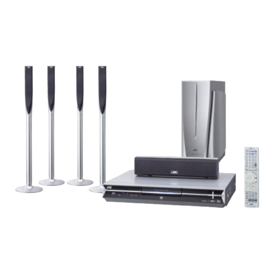
DVD DIGITAL CINEMA SYSTEM
SP-THS66F
SP-THS66F SP-THS66S
SP-THS66C
Lead free solder used in the board (material : Sn-Ag-Cu, melting point : 219 Centigrade)
Contents
Wiring diagram
Block diagrams
Standard schematic diagrams
Printed circuit boards
TH-R3, TH-R1
CD-ROM No.SML200508
SP-PWR3
1
2
4
5
7
8
0
ENTER
VOL
SOURCE
XV-THR3
COPYRIGHT
2005 Victor Company of Japan, Limited.
B ------------------------------ U.K.
E ---------- Continental Europe
EN ----------- Northern Europe
EV ------------- Eastern Europe
EE -------- Russian Federation
EF --------------------------France
EL ------------ Southern Europe
SP-THS55C
SP-THS55S
SP-THS55F
3
6
9
VOL
XV-THR1
Area suffix
SP-PWR1
1
2
3
4
5
6
7
8
9
0
VOL
ENTER
VOL
SOURCE
2-1
2-2
2-5
2-26 to 30
No.MB442BSCH
2005/8
Advertisement
Table of Contents

Related Manuals for JVC SP-PWR3


Summarization of Contents
Block Diagrams
Audio Signal Control Section
Diagrams detailing the audio signal control circuitry.
Video Signal Control Section
Diagrams for video signal control and switching.
Input/Output Terminal Section
Schematics for system input and output terminals.
System Controller Section
Diagrams for the main system controller (SYSCON).
Tuner Section
Diagrams detailing the tuner circuitry.
Input/Output Relay Section
Schematics of input/output relay functions.
Demodulator Section
Diagrams for the demodulator circuit.
FL Display and Operation Switch Section
LED Section
Schematic for LED indicators.
SW/JACK Section
Schematics for switch and jack connections.
DV JACK Section
Schematic for the DV jack.
RGB-Y/C Converter Section
RGB-Y/C converter schematic.
Standard Schematic Diagrams
Power Supply Section
Schematic for the power supply unit.
Need help?
Do you have a question about the SP-PWR3 and is the answer not in the manual?
Questions and answers