Table of Contents
Advertisement
HISTORY INFORMATION FOR THE FOLLOWING MANUAL:
SERVICE MANUAL
RB1FK
Segments: BL
ORIGINAL MANUAL ISSUE DATE: 12/2013
REVISION DATE
12/9/2013
9-883-557-51
CHASSIS
SUBJECT
Original Manual Release Date
MODEL
COMMANDER
KDL-50R550A
RM-YD094
KDL-50R550A
RM-YD094
KDL-50R555A
RM-YD095
KDL-50R557A
RM-YD095
KDL-60R520A
RM-YD096
KDL-60R550A
RM-YD094
KDL-60R550A
RM-YD094
KDL-60R551A
RM-YD094
KDL-60R555A
RM-YD094
KDL-60R557A
RM-YD094
KDL-70R520A
RM-YD096
KDL-70R550A
RM-YD094
KDL-70R550A
RM-YD094
KDL-70R551A
RM-YD094
KDL-70R555A
RM-YD094
KDL-70R557A
RM-YD094
Self Diagnosis
DESTINATION
US / Canada
Mexico / Latin America
Chile / Peru / Venezuela
Colombia
US / Canada
US / Canada
Mexico / Latin America
Mexico / Latin America
Chile / Peru / Venezuela
Colombia
US
US / Canada
Mexico / Latin America
Mexico / Latin America
Chile / Peru / Venezuela
Colombia
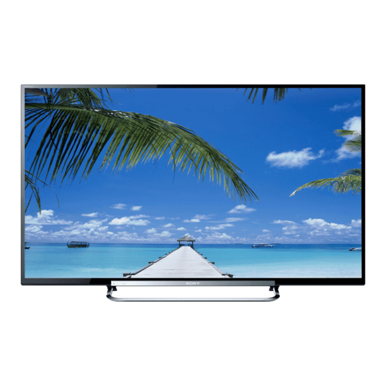
LCD DIGITAL COLOR TV
Supported model
Advertisement
Table of Contents

Summarization of Contents
SETTING UP AND CARRYING THE TV
USE CAUTION WHEN HANDLING THE LCD PANEL
Guidelines for preventing damage to the LCD panel during servicing.
CLEANING THE LCD PANEL
Procedures for safely cleaning the television's screen and cabinet.
SAFETY CHECK-OUT
LEAKAGE TEST
Method for testing electrical leakage current to prevent shock hazards.
HOW TO FIND A GOOD EARTH GROUND
Procedure to verify a proper earth ground connection for safety testing.
SECTION 1: DIAGRAMS
1-1. PRINTED CIRCUIT BOARDS AND SCHEMATIC DIAGRAMS INFORMATION
Explains symbols, notations, and conventions used in diagrams.
1-2. CIRCUIT BOARDS LOCATION
Visual identification of main circuit boards within the TV chassis.
1-3. CONNECTOR DIAGRAMS
Pin assignments and connection details for all internal connectors.
1-4. MAIN BOARD (A BOARD)
Component layout and conductor traces for the primary system board.
A BOARD SCHEMATIC DIAGRAMS INDEX
Index of schematic diagrams covering various A Board functions and interfaces.
VGA Interface
Details for the Video Graphics Array input port and circuitry.
HDMI Interface I
Information on the first High-Definition Multimedia Interface.
RF TUNER AND DEMODULATOR DATA
Specifications for RF tuner and demodulator modules across regions.
USB AND WIFI INTERFACES
Details for USB multimedia and Wi-Fi module interface signals.
AUDIO AND SPEAKER CIRCUITS
Schematics for audio amplifier control, muting, and speaker protection.
PANEL AND TCON CONTROL
Control signals for TCON power and LCD panel identification.
I/O for USB WIFI Module
Interface signals for the USB Wi-Fi module.
SECTION 2: POWER SUPPLY BOARD (G BOARD)
G BOARD SCHEMATIC
Detailed schematic diagrams for the power supply board.
SECTION 3: IR BOARD (H BOARD)
H BOARD COMPONENT SIDE
Component layout of the IR receiver board.
H BOARD CONDUCTOR SIDE
Conductor traces for the IR receiver board.


Need help?
Do you have a question about the KDL-70R555A and is the answer not in the manual?
Questions and answers