Table of Contents
Advertisement
RX-V1300/RX-V1300RDS/HTR-5590/DSP-AX1300
This manual has been provided for the use of authorized YAMAHA Retailers and their service personnel.
It has been assumed that basic service procedures inherent to the industry, and more specifically YAMAHA Products, are already
known and understood by the users, and have therefore not been restated.
WARNING:
IMPORTANT:
The data provided is believed to be accurate and applicable to the unit(s) indicated on the cover. The research, engineering, and
service departments of YAMAHA are continually striving to improve YAMAHA products. Modifications are, therefore, inevitable
and specifications are subject to change without notice or obligation to retrofit. Should any discrepancy appear to exist, please
contact the distributor's Service Division.
WARNING:
IMPORTANT:
I CONTENTS
TO SERVICE PERSONNEL .......................................... 2
IMPEDANCE SELECTOR ............................................. 2
FRONT PANELS ........................................................ 3~4
REAR PANELS .......................................................... 5~9
REMOTE CONTROL ...................................................... 9
SPECIFICATIONS .................................................. 10~12
INTERNAL VIEW ......................................................... 13
DISASSEMBLY PROCEDURES / 分解手順 ......... 14~18
自己診断機能(ダイアグ) ..................................... 19~45
1 0 0 8 1 6
AV RECEIVER/AV AMPLIFIER
IMPORTANT NOTICE
Failure to follow appropriate service and safety procedures when servicing this product may result in personal
injury, destruction of expensive components, and failure of the product to perform as specified. For these reasons,
we advise all YAMAHA product owners that any service required should be performed by an authorized
YAMAHA Retailer or the appointed service representative.
The presentation or sale of this manual to any individual or firm does not constitute authorization, certification or
recognition of any applicable technical capabilities, or establish a principle-agent relationship of any form.
Static discharges can destroy expensive components. Discharge any static electricity your body may have
accumulated by grounding yourself to the ground buss in the unit (heavy gauge black wires connect to this buss).
Turn the unit OFF during disassembly and part replacement. Recheck all work before you apply power to the unit.
RX-V2300/DSP-AX2300
SERVICE MANUAL
AMP ADJUSTMENT / アンプ部調整 ..................... 46~47
DISPLAY DATA ..................................................... 48~49
IC DATA ................................................................. 50~53
BLOCK DIAGRAM ................................................. 54~55
PRINTED CIRCUIT BOARD .................................. 56~81
PIN CONNECTION DIAGRAM .................................... 82
SCHEMATIC DIAGRAM ........................................ 83~92
PARTS LIST ......................................................... 93~153
REMOTE CONTROL .......................................... 154~159
Parts List for Carbon Resistors .............................. 160
P.O.Box 1, Hamamatsu, Japan
Advertisement
Table of Contents

Related Manuals for Yamaha DSP-AX1300


Summarization of Contents
To Service Personnel
Critical Components Information
Information about components requiring specific replacement parts.
Leakage Current Measurement (For 120V Models Only)
Procedure for verifying insulation of conductive surfaces from supply circuits.
Front Panels
RX-V2300 (U, C, A, R, T, K models)
Front panel view for RX-V2300 models in specific regions.
DSP-AX2300 (J model)
Front panel view for the DSP-AX2300 J model.
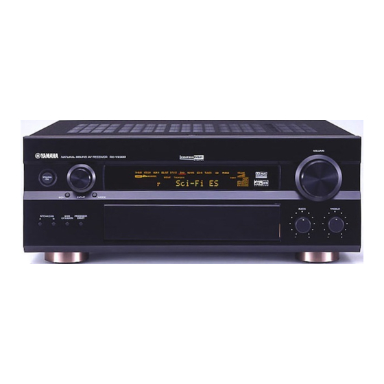
RX-V1300 (U, C, A, R, T, K models)
Front panel view for RX-V1300 models in specific regions.
Rear Panels
RX-V2300 (U, C models)
Rear panel view for RX-V2300 U and C models.
RX-V2300 (A model)
Rear panel view for RX-V2300 A model.
RX-V2300 (R, T, K models)
Rear panel view for RX-V2300 R, T, and K models.
Remote Control
RX-V2300/DSP-AX2300
Remote control layout for RX-V2300 and DSP-AX2300 models.
RX-V1300/HTR-5590/DSP-AX1300 (U, C, A, R, T, K, J models)
Remote control layout for various RX-V1300/HTR-5590/DSP-AX1300 models.
RX-V1300RDS (B, G models)
Remote control layout for RX-V1300RDS B and G models.
Specifications / 参考仕様
Audio Section / オーディオ部
Detailed audio performance specifications including output power and frequency response.
Video Section / ビデオ部
Detailed video signal specifications including levels and response.
FM Section / FM部
Detailed FM tuner specifications including sensitivity and selectivity.
Disassembly Procedure / 分解手順
Removal of Top Cover
Procedure for removing the top cover of the unit.
Removal of Front Panel
Procedure for removing the front panel assembly.
Removal of Sub Chassis
Procedure for removing the sub chassis component.
Removal of DSP P.C.B.
Procedure for removing the DSP printed circuit board.
Removal of VIDEO (5) P.C.B.
Procedure for removing the VIDEO (5) P.C.B.
Self Diagnosis Function (DIAG)/自己診断機能(ダイアグ)
Starting DIAG
Instructions for initiating the diagnostic mode via unit buttons.
Starting DIAG in the protection cancel mode
Procedure for entering diagnostic mode with protection function disabled.
Canceling DIAG
Steps to cancel the diagnostic mode and return to normal operation.
Details of DIAG menu
1. YSS938
Details of the YSS938 diagnostic function, including bypass and output levels.
YSS FULL BIT
Details on digital full bit output for YSS, excluding head margin.
DSP BYPASS
Details on the DSP bypass function for YSS analog signals.
2. YSS-SD
Details of the YSS-SD diagnostic function, including channel output and bit settings.
3. SD-YSS
Details of the SD-YSS diagnostic function, including channel output and bit settings.
4. SECOND DECODER
Details of the second decoder function, including output modes and DTS ES considerations.
5. HP ROUTE
Details of the HP route diagnostic function for YSS938 output.
6. RAM THROUGH
Details of the RAM THROUGH diagnostic function for YSS938 output.
7. PRO LOGIC / NEO6
Details of PRO LOGIC I, II, and NEO6 processing functions.
Neo:6
Details of the Neo:6 processing function, fixed to Cinema 6ch mode.
8. SPEAKERS SET
Settings for speaker configuration including size and signal output.
10. MANUAL TEST
TEST ALL
Noise output test for all channels.
TEST MAIN L
Noise output test for the main L channel.
TEST CENTER
Noise output test for the center channel.
TEST MAIN R
Noise output test for the main R channel.
TEST REAR L
Noise output test for the rear L channel.
TEST REAR R
Noise output test for the rear R channel.
TEST REAR C
Noise output test for the rear C channel.
TEST LFE
Noise output test for the sub woofer channel.
11. RS-232C
TxD/RxD DATA
Sub-menu for checking test data transmission.
HARD FLOW
Sub-menu for checking hardware flow port operation.
13. AD DATA CHECK / FAN TEST
DC/PS (protection detection)
Sub-menu for DC and PS protection value detection.
THM/FAN OUT (temperature detection/fan drive level)
Sub-menu for temperature detection and fan drive level.
REC-OUT (Select position)
Sub-menu for selecting REC OUT position.
17. SOFT SW
SW MODE
Option to select between PCB and SOFT mode.
MODEL SETTING
Setting for selecting the model number.
TUNER DESTINATION
Setting for selecting the tuner destination.
TUNER EXIST
Setting to indicate if tuner exists.
RDS EXIST
Setting to indicate if RDS exists.
ZONE 2 EXIST
Setting to indicate if Zone 2 exists.
VIDEO FORMAT
Setting for selecting video format (NTSC or PAL).
AMP ADJUSTMENT / アンプ部調整
Confirmation of Idling Current of Main (1) and (2) P.C.B.
Procedure to confirm idling current across terminals of main PCBs.
DISPLAY DATA
PIN CONNECTION
Pin connection details for various components.
GRID ASSIGNMENT
Diagram illustrating grid assignment for display elements.
Printed Circuit Board (Foil side)
DSP P.C.B. (Lead Type Device)
Foil side view of the DSP PCB with lead type components.
DSP P.C.B. (Surface Mount Device)
Foil side view of the DSP PCB with surface mount devices.
FUNCTION P.C.B. (Lead Type Device)
Foil side view of the FUNCTION PCB with lead type components.
FUNCTION P.C.B. (Surface Mount Device)
Foil side view of the FUNCTION PCB with surface mount devices.
OPERATION (1) P.C.B. (Lead Type Device)
Foil side view of OPERATION (1) PCB with lead type components.
OPERATION (1) P.C.B. (Surface Mount Device)
Foil side view of OPERATION (1) PCB with surface mount devices.
OPERATION (2) P.C.B. (Lead Type Device)
Foil side view of OPERATION (2) PCB with lead type components.
OPERATION (2) P.C.B. (Surface Mount Device)
Foil side view of OPERATION (2) PCB with surface mount devices.
OPERATION (3) P.C.B. (Lead Type Device)
Foil side view of OPERATION (3) PCB with lead type components.
OPERATION (4) P.C.B. (Lead Type Device)
Foil side view of OPERATION (4) PCB with lead type components.
OPERATION (4) P.C.B. (Surface Mount Device)
Foil side view of OPERATION (4) PCB with surface mount devices.
OPERATION (5) P.C.B. (Lead Type Device)
Foil side view of OPERATION (5) PCB with lead type components.
OPERATION (5) P.C.B. (Surface Mount Device)
Foil side view of OPERATION (5) PCB with surface mount devices.
OPERATION (4) P.C.B. (Lead Type Device)
Foil side view of OPERATION (4) PCB with lead type components.
VIDEO (1) P.C.B. (Lead Type Device)
Foil side view of VIDEO (1) PCB with lead type components.
VIDEO (1) P.C.B. (Surface Mount Device)
Foil side view of VIDEO (1) PCB with surface mount devices.
VIDEO (2) P.C.B. (Lead Type Device)
Foil side view of VIDEO (2) PCB with lead type components.
VIDEO (2) P.C.B. (Surface Mount Device)
Foil side view of VIDEO (2) PCB with surface mount devices.
VIDEO (4) P.C.B. (Lead Type Device)
Foil side view of VIDEO (4) PCB with lead type components.
VIDEO (4) P.C.B. (Surface Mount Device)
Foil side view of VIDEO (4) PCB with surface mount devices.
VIDEO (5) P.C.B. (Lead Type Device)
Foil side view of VIDEO (5) PCB with lead type components.
VIDEO (5) P.C.B. (Surface Mount Device)
Foil side view of VIDEO (5) PCB with surface mount devices.
VIDEO (6) P.C.B. (Lead Type Device)
Foil side view of VIDEO (6) PCB with lead type components.
VIDEO (6) P.C.B. (Surface Mount Device)
Foil side view of VIDEO (6) PCB with surface mount devices.
VIDEO (7) P.C.B. (Lead Type Device)
Foil side view of VIDEO (7) PCB with lead type components.
VIDEO (8) P.C.B. (Lead Type Device)
Foil side view of VIDEO (8) PCB with lead type components.
VIDEO (1) P.C.B. (Lead Type Device)
Foil side view of VIDEO (1) PCB with lead type components.
VIDEO (1) P.C.B. (Surface Mount Device)
Foil side view of VIDEO (1) PCB with surface mount devices.
MAIN (1) P.C.B. (Lead Type Device)
Foil side view of MAIN (1) PCB with lead type components.
MAIN (2) P.C.B. (Lead Type Device)
Foil side view of MAIN (2) PCB with lead type components.
MAIN (3) P.C.B. (Lead Type Device)
Foil side view of MAIN (3) PCB with lead type components.
MAIN (4) P.C.B. (Lead Type Device)
Foil side view of MAIN (4) PCB with lead type components.
MAIN (5) P.C.B. (Lead Type Device)
Foil side view of MAIN (5) PCB with lead type components.
MAIN (6) P.C.B. (Lead Type Device)
Foil side view of MAIN (6) PCB with lead type components.
POWER (1) P.C.B. (Lead Type Device)
Foil side view of POWER (1) PCB with lead type components.
POWER (2) P.C.B. (Lead Type Device)
Foil side view of POWER (2) PCB with lead type components.
POWER (3) P.C.B. (Lead Type Device)
Foil side view of POWER (3) PCB with lead type components.
POWER (4) P.C.B. (Lead Type Device)
Foil side view of POWER (4) PCB with lead type components.
POWER (5) P.C.B. (Lead Type Device)
Foil side view of POWER (5) PCB with lead type components.
POWER (6) P.C.B. (Lead Type Device)
Foil side view of POWER (6) PCB with lead type components.
Pin Connection Diagram
ICs
Pin connection diagrams for integrated circuits.
Diodes
Pin connection diagrams for diodes.
Transistors
Pin connection diagrams for transistors.
Electrical Parts
P.C.B. DSP
Electrical parts list for the DSP P.C.B.
P.C.B. FUNCTION
Electrical parts list for the FUNCTION P.C.B.
P.C.B. OPERATION
Electrical parts list for the OPERATION PCB.
P.C.B. VIDEO
Electrical parts list for the VIDEO PCB.
P.C.B. MAIN
Electrical parts list for the MAIN PCB.
Mechanical Parts
P.C.B. ASS'Y MAIN
Part number and description for main PCB assemblies.
P.C.B. ASS'Y FUNCTION
Part number and description for function PCB assemblies.
P.C.B. ASS'Y POWER
Part number and description for power PCB assemblies.
P.C.B. ASS'Y DSP
Part number and description for DSP PCB assemblies.
FRONT PANEL & SUB CHASSIS UNIT
List of parts for the front panel and sub chassis unit.
AMP UNIT
Parts list for the amplifier unit.
Need help?
Do you have a question about the DSP-AX1300 and is the answer not in the manual?
Questions and answers