Table of Contents
Advertisement
SERVICE MANUAL
Ver. 1.1 2010.05
• HBD-TZ210/TZ230/TZ510/TZ630/TZ710 are the amplifi er,
DVD/CD and tuner section in DAV-TZ210/TZ230/TZ510/
TZ630/TZ710.
This system incorporates with Dolby* Digital and Dolby Pro Logic
(II) adaptive matrix surround decoder and the DTS** Digital Surround
System.
* Manufactured under license from Dolby Laboratories.
Dolby, Pro Logic, and the double-D symbol are trademarks of
Dolby Laboratories.
** Manufactured under license under U.S. Patent #'s:
5,451,942; 5,956,674; 5,974,380; 5,978,762; 6,487,535 & other
U.S. and worldwide patents issued & pending. DTS and DTS
Digital Surround are registered trademarks and the DTS logos and
Symbol are trademarks of DTS, Inc. © 1996-2008 DTS, Inc. All
Rights Reserved.
Amplifi er Section
(DAV-TZ210/DAV-TZ510/DAV-TZ710)
POWER OUTPUT (rated):
Front L + Front R
65 W + 65 W (at 3 ohms, 1
kHz, 1% THD)
POWER OUTPUT (reference):
Front L/Front R/Center/
Surround L/Surround R:
100 watts (per channel at 3
ohms, 1 kHz)
Subwoofer: 100 watts (at 3
ohms, 80 Hz)
Inputs (Analog)
Canadian model:
TV/CABLE (AUDIO IN)
Sensitivity: 450/250 mV
Other models:
TV (AUDIO IN)
Sensitivity: 450/250 mV
Amplifi er Section
(DAV-TZ230/DAV-TZ630)
POWER OUTPUT (rated):
Front L + Front R
65 W + 65 W (at 3 ohms, 1
kHz, 1% THD)
POWER OUTPUT (reference):
Front L/Front R/Center/
Surround L/Surround R:
100 watts (per channel at 3
ohms, 1 kHz)
Subwoofer: 100 watts (at 3
ohms, 80 Hz)
Inputs (Analog)
TV (AUDIO IN)
Sensitivity: 450/250 mV
Sony Corporation
9-889-755-02
2010E04-1
Audio&Video Business Group
©
2010.05
Published by Sony Techno Create Corporation
HBD-TZ210/TZ230/TZ510/
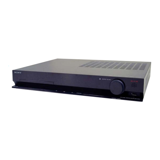
Photo: HBD-TZ210
Model Name Using Similar Mechanism
Mechanism Type
Optical Pick-up Name
SPECIFICATIONS
Super Audio CD/DVD System
(DAV-TZ210/DAV-TZ510/DAV-TZ710)
Laser Diode Properties
Emission Duration:
Continuous
Laser Output: Less than
44.6 W
* This output is the value measurement at a distance
of 200 mm from the objective lens surface on the
Optical Pick-up Block with 7 mm aperture.
Signal format system
Mexican and Latin American models:
NTSC
Other models:
NTSC/PAL
Super Audio CD/DVD System
(DAV-TZ230/DAV-TZ630)
Laser Diode Properties
Emission Duration:
Continuous
Laser Output: Less than
44.6 W
* This output is the value measurement at a distance
of 200 mm from the objective lens surface on the
Optical Pick-up Block with 7 mm aperture.
Signal format system
PAL/NTSC
USB Section
(USB) port:
Maximum current:
500 mA
TZ630/TZ710
Canadian Model
HBD-TZ210/TZ510
AEP Model
HBD-TZ230/TZ630
UK Model
HBD-TZ230
E Model
HBD-TZ210/TZ510/TZ710
Australian Model
HBD-TZ210
Chinese Model
HBD-TZ710
Russian Model
HBD-TZ210/TZ710
HBD-DZ170/DZ171/DZ175/
DZ310/DZ510/DZ610/DZ810
CDM85MB-DVBU102
KHM-313CAA
Tuner Section
System
PLL quartz-locked digital
synthesizer
Tuning range
Canadian model:
87.5 MHz - 108.0 MHz
(100 kHz step)
Other models:
87.5 MHz - 108.0 MHz (50
kHz step)
Antenna (aerial)
FM wire antenna (aerial)
Antenna (aerial) terminals 75 ohms, unbalanced
Intermediate frequency
10.7 MHz
Video Section
(DAV-TZ210/DAV-TZ510/DAV-TZ710)
Outputs
VIDEO: 1 Vp-p 75 ohms
HDMI OUT: Type A (19
pin)
Video Section
(DAV-TZ230/DAV-TZ630)
Outputs
VIDEO: 1 Vp-p 75 ohms
R/G/B: 0.7 Vp-p 75 ohms
HDMI OUT: Type A (19
pin)
– Continued on next page –
DVD RECEIVER
Advertisement
Table of Contents

Related Manuals for Sony HBD-TZ230


Summarization of Contents
Specifications
Amplifier Section
Technical specifications for the amplifier section.
Super Audio CD/DVD System
Specifications for the Super Audio CD/DVD system.
Tuner Section
Technical specifications for the tuner section.
Video Section
Technical specs for the video output section.
USB Section
Specifications for the USB interface.
General Information and Warnings
Supported File Formats
List of supported audio and video file formats.
Safety Component Warning
Critical warning about components essential for safe operation.
Special Component Notice
Notice regarding components containing confidential information.
Servicing Precautions and Procedures
Cautionary Notes
Warning about hazardous radiation exposure from improper controls.
Chip Component Replacement Notes
Guidelines for replacing chip components, including tantalum capacitor care.
Flexible Circuit Board Repair
Procedures for repairing flexible circuit boards, including soldering temperatures.
Unleaded Solder Handling
Information on using unleaded solder, including its characteristics and handling.
Lead Free Mark Identification
Explanation of the lead-free mark (LF) on PCBs.
Self-Diagnosis Function
Display Test Mode
Test mode to check all segments of the display.
Version Test Mode
Mode to display software version and destination information.
FL Pattern Test Mode
Test mode to check FL display segments.
Key Test Mode
Mode to test system keys and fluorescent indicator.
Model Identification
Abbreviation List
List of abbreviations used for regional model designations.
Servicing Notes
Notes on Handling Optical Pick-up
Precautions for handling the optical pick-up block and base unit.
Laser Diode Emission Check
Precautions for checking laser diode emission to avoid hazardous radiation.
Disc Tray Lock Function
Procedure for locking and unlocking the disc tray for anti-theft.
Important Notice on Screen Damage
Caution regarding potential permanent damage to TV screens from static images.
Disassembly Procedures
2-1. Case Removal
Procedure for removing the outer case of the unit.
2-2. Loading Panel Disassembly
Steps to disassemble the disc loading panel mechanism.
2-3. Front Panel Section Removal
Procedure for removing the front panel assembly.
2-4. Board Removal (FL, USB KEY, USB)
Steps to remove the FL, USB KEY, and USB boards.
2-5. Board Removal (KEY-SW, P-SW)
Procedure for removing the KEY-SW and P-SW boards.
2-6. Back Panel Section Removal (TZ230/TZ630)
Steps to remove the back panel for specific models.
2-7. Back Panel Section Removal (TZ210/TZ510/TZ710)
Steps to remove the back panel for other models.
2-8. Main Board Access
Procedure for accessing and removing the main board.
2-9. Power Board Removal
Steps to remove the power board.
2-10. DVD Mechanism Deck Removal
Procedure for removing the DVD mechanism deck assembly.
2-11. Tray Removal
Steps to remove the disc tray from the mechanism.
2-12. Belt Replacement
Procedure for removing or replacing the drive belt.
2-13. MS-203 Board Removal
Steps to remove the MS-203 board.
2-14. Base Unit Removal
Procedure for removing the base unit.
2-15. Optical Pick-up Removal
Steps to remove the optical pick-up assembly.
Test Mode Procedures
Cold Reset Function
Procedure to clear all data and reset the system to initial conditions.
Panel Test Modes
Modes to check software version, FL display, and keys.
Disc Tray Lock Operation
Setting and releasing the disc tray lock function.
DVD Version Display
Displaying STR and DVD microprocessor versions.
Product Out Mode
Mode to move optical pick-up and clear data for customer return.
Advanced Test Mode Functions
Color System Change
Changing color system to video signal format (NTSC/PAL).
Protection Factor Test Mode
Test mode to identify protection factors like SD, DC, or TSD detection.
Entering Test Mode
Procedure to enter the test mode via remote commander.
IOP Measurement Execution
Standard procedures for executing IOP measurement.
Emergency History Check
Emergency History Check
Procedure to check emergency history and error codes.
Version Information and Data Management
Version Information Check
Procedure to check firmware version information.
Laser Hour Counter Reset
Procedure to reset the laser hour counter for CD and DVD.
Emergency History Clear
Procedure to clear all emergency history error codes.
Initialize Setup Data
Procedure to clear and initialize system setup data.
Electrical Adjustments
IOP Measurement Execution
Perform IOP measurement after replacing the optical pick-up.
FM Tune Level Check
Procedure for checking FM tuner sensitivity and reception.
Diagrams and Board Locations
Printed Wiring Board Notes
Notes and symbols used for printed wiring board diagrams.
Schematic Diagram Notes
Notes and symbols used for schematic diagrams.
Circuit Board Locations
Diagram showing the location of main circuit boards.
Block Diagrams
5-1. Block Diagram - RF Section
Block diagram illustrating the RF signal path.
5-2. Block Diagram - Video Section
Block diagram showing the video signal processing path.
5-3. Block Diagram - Audio Section
Block diagram illustrating the audio signal path.
5-4. Block Diagram - AMP Section
Block diagram of the amplifier section, showing power and signal paths.
5-5. Block Diagram - Power Section
Block diagram of the power supply section.
Waveform Analysis
Main Board Waveforms
Oscilloscope waveforms for key points on the MAIN board.
SCART Board Waveforms
Oscilloscope waveforms for points on the SCART board.
Printed Wiring Board Layouts
5-6. Printed Wiring Board - Main Section (1/2)
Printed wiring board layout for the main board (part 1).
5-7. Printed Wiring Board - Main Section (2/2)
Printed wiring board layout for the main board (part 2).
5-16. Printed Wiring Board - SCART Section
Printed wiring board layout for the SCART board.
5-18. Printed Wiring Board - FL Section
Printed wiring board layout for the FL display board.
5-20. Printed Wiring Boards (KEY-SW, P-SW, USB, USB KEY)
Printed wiring board layouts for KEY-SW, P-SW, USB, USB KEY boards.
5-23. Printed Wiring Board - Power Section
Printed wiring board layout for the power board.
Schematic Diagrams
5-8. Schematic Diagram - Main Section (1/8)
Schematic diagram of the main board (section 1 of 8).
5-9. Schematic Diagram - Main Section (2/8)
Schematic diagram of the main board (section 2 of 8).
5-10. Schematic Diagram - Main Section (3/8)
Schematic diagram of the main board (section 3 of 8).
5-11. Schematic Diagram - Main Section (4/8)
Schematic diagram of the main board (section 4 of 8).
5-12. Schematic Diagram - Main Section (5/8)
Schematic diagram of the main board (section 5 of 8).
5-13. Schematic Diagram - Main Section (6/8)
Schematic diagram of the main board (section 6 of 8).
5-14. Schematic Diagram - Main Section (7/8)
Schematic diagram of the main board (section 7 of 8).
5-15. Schematic Diagram - Main Section (8/8)
Schematic diagram of the main board (section 8 of 8).
5-17. Schematic Diagram - SCART Section
Schematic diagram for the SCART board.
5-19. Schematic Diagram - FL Section
Schematic diagram for the FL display board.
5-21. Schematic Diagram - KEY-SW, P-SW Section
Schematic diagrams for KEY-SW and P-SW boards.
5-22. Schematic Diagram - USB, USB KEY Section
Schematic diagrams for USB and USB KEY boards.
5-24. Schematic Diagram - Power Section
Schematic diagram for the power board.
IC Block Diagrams
Voltage Regulator and Control ICs
Block diagrams for voltage regulator and control ICs.
Audio Interface IC Block Diagram
Block diagram for the IC504 audio interface chip.
Motor Driver IC Block Diagram
Block diagram for the IC1501 motor driver IC.
Voltage Regulator IC Block Diagrams
Block diagrams for voltage regulator ICs.
Audio ADC IC Block Diagram
Block diagram for the IC404 audio ADC chip.
S-MASTER Processor IC Block Diagrams
Block diagrams for the IC3001/3003/3005 S-MASTER processors.
Digital Power Amplifier IC Block Diagrams
Block diagrams for IC3000/3002/3004 digital power amplifier ICs.
Analog Multiplexer IC Block Diagram
Block diagram for the IC401 analog multiplexer.
Video Driver IC Block Diagram
Block diagram for the IC4000 video driver chip.
Switching Regulator IC Block Diagram
Block diagram for IC901 switching regulator.
IC Pin Function Descriptions
Main Board IC1101 Pin Functions
Pin function description for IC1101 on the main board.
Main Board IC503 Pin Functions
Pin function description for IC503 SYSTEM CONTROL on the main board.
Main Board IC1101 Pin Functions (Continued)
Continued pin function descriptions for IC1101.
Main Board IC503 Pin Functions (Continued)
Continued pin function descriptions for IC503.
Main Board IC503 Pin Functions (Continued)
Continued pin function descriptions for IC503.
Main Board IC503 Pin Functions (Continued)
Continued pin function descriptions for IC503.
Exploded Views
Overall Section Exploded View
Exploded view of the overall unit with parts list.
Front Panel Section Exploded View
Exploded view of the front panel assembly with parts list.
Front Boards Section Exploded View
Exploded view of front boards and associated wiring with parts list.
Chassis Section Exploded View
Exploded view of the chassis and main boards with parts list.
DVD Mechanism Deck Section Exploded View
Exploded view of the DVD mechanism deck with parts list.
Electrical Parts List
FL Board Parts List
List of electrical parts for the FL board.
Component Lists (Capacitors, Coils, Semiconductors, Resistors)
Lists of common electronic components used in the unit.
KEY-SW and Main Board Parts List
Electrical parts list for the KEY-SW and MAIN boards.
Capacitor Lists
List of capacitors for various boards.
Main Board Capacitor List
List of capacitors for the main board.
Main Board Capacitor List (Continued)
Continued list of capacitors for the main board.
Main Board Capacitor List (Continued)
Continued list of capacitors for the main board.
Connector and Diode Lists
List of connectors and diodes used in the unit.
Ferrite Bead and Transformer Lists
List of ferrite beads and transformers.
IC, Jack, Coil, Transistor, Resistor Lists
Lists of integrated circuits, jacks, coils, transistors, and resistors.
Resistor List (Continued)
Continued list of resistors.
Resistor List (Continued)
Continued list of resistors.
Resistor List (Continued)
Continued list of resistors.
Network Resistors and Terminal Board Parts
Lists of network resistors and terminal board components.
Vibrator, MS-203 Board, Connector, Switch Lists
Lists of vibrator, MS-203 board, connector, and switch parts.
Power Board Parts List
List of parts for the power board.
Diode, Capacitor, Connector, Switch Lists
Lists of diodes, capacitors, connectors, and switches.
Diode, Fuse, Fuse Holder, Resistor, IC, Coil Lists
Lists of diodes, fuses, holders, resistors, ICs, and coils.
Line Filter, Photo Coupler, Transistor, Varistor Lists
Lists of line filters, photo couplers, transistors, and varistors.
SCART Board Parts List
List of parts for the SCART board.
IC, Transformer, Transistor, Resistor Lists
Lists of ICs, transformers, transistors, and resistors.
USB Board Parts List
List of parts for the USB board.
USB Key Board Parts List
List of parts for the USB KEY board.
Rotary Encoder, Switch, Miscellaneous Lists
Lists of rotary encoder, switches, and miscellaneous parts.
Need help?
Do you have a question about the HBD-TZ230 and is the answer not in the manual?
Questions and answers