Table of Contents
Advertisement
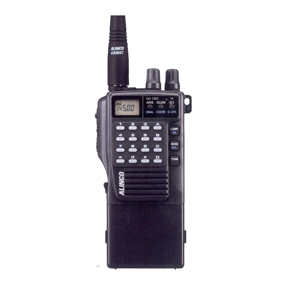
DJ-180
DJ-1400
CONTENTS
SEMICONDUCTOR DATA
1) LR408721
2) M5218FP
3) M5236ML.
4) MB1504LPF
5) MC3357
6) MX365
7) NJM386
8) RH5VA32AA.
10) X24C01A
11) X24C04S14
12) X24C16S14
13) Transistor, Diode and LED Outline Draw
14) LCD Connection.
EXPLODED VIEW
3) Rear Case 2
4) Front Case 1
5) Front Case 2
6) Front Case 3 and Battery Terminal
7) Ten Key Cover and Key Pad Panel
8) CTCSS Unit and ROM1 Unit
Service Manual
PC BOARD VIEW
2
1) VCO Unit
2
2) JACK Unit
2
3) PTT Unit Side B
3
4) PS Unit
5) ROM1 Unit Side B
4
6) ROM2 Unit Side B
5
7) RF Unit Side A
5
8) RF Unit Side B
6
9) CPU Unit Side A.
6
10) CPU Unit Side B
6
11) RE Unit
7
12) CTCSS UniL
13) DTMF Unit.
10
10
CPU unit
10
PS unit.
11
ROM1 Unit
11
DTMF Unit
12
RF Unit
13
13
13
14
14
14
15
16
Parts Table for Each Version.
17
17
1) Required Test Equipment.
18
2) Before Adjustment
19
20
21
5) Adjustment Quick Reference
22
6) Adjustment Points.
23
CIRCUIT DIAGRAM
BLOCK DIAGRAM
ALINCO INCORPORATED
TWIN 21 M.I.D. TOWER
SHIROMI CHUO-KU , OSAKA,
6-
946-8150
Tel (81)
6
e-mail: export@alinco.co.jp
BUILDING 23F, 1-61, 2-CHOME,
540-8580 JAPAN
fax (81)6-6946-8175
24
24
24
25
25
25
26
27
28
29
30
30
31
32
32
33
33
33 ~ 36
37
37
38
38
38
38
38
38
39
40
40
41
42
43
43 ~ 44
45 ~ 46
47
Advertisement
Table of Contents

Related Manuals for Alinco DJ-1400


Summarization of Contents
Service Manual
Specifications
Detailed technical specifications for the radio models.
General (DJ-180)
General specifications including frequency coverage, resolution, memory channels, etc.
Transmitter (DJ-180)
Transmitter output power, modulation system, frequency deviation, and tone settings.
Receiver (DJ-180)
Receiver system, intermediate frequencies, and sensitivity details.
General (DJ-1400QN/AN)
General specifications for narrow version models.
Transmitter (DJ-1400QN/AN)
Transmitter specs for narrow version models.
Receiver (DJ-1400QN/AN)
Receiver specs for narrow version models.
Circuit Description
Receiver System
Detailed description of the double superheterodyne receiver system.
Receiver Front End
Signal path from antenna through RF coil and mixer.
First Mixer
Mixing of RF signal with local oscillator for first IF.
IF Amplifier
Amplification and conversion to the second IF signal.
Audio Circuit
Processing of detected audio signal and amplification.
Squelch Circuit
Noise gating and signal detection for squelch operation.
PLL, VCO Circuit
PLL circuit operation for frequency setting and VCO tuning.
Transmitter System
Microphone amplifier, power amplifier, and APC circuit.
Microprocessor (CPU) and Peripheral Circuit
CPU operation modes, backup, and reset functions.
Semiconductor Data
LR408721 (Tone Dialer)
Details and test circuit for the tone dialer IC.
M5218FP (Dual Low Noise Operational Amplifiers)
Pinout and description of dual op-amp IC.
M5236ML (Voltage Regulator)
Pinout and test circuit for the voltage regulator IC.
MB1504LPF-G-BND-TF (Frequency Synthesizer)
Function table and pinout for the frequency synthesizer.
MC3357 (Narrow Band FM IF IC)
Electrical characteristics and block diagram of the IF IC.
MX365 (CTCSS Encoder/Decoder)
Pin descriptions and functions of the CTCSS IC.
NJM386 (Dual Power Amplifiers)
Pinout and description of dual power amplifier IC.
RH5VA32AA-T1 (C-MOS Voltage Detector)
Pinout and equivalent circuit for voltage detector.
RH5VA45AA-T1 (C-MOS Voltage Detector)
Pinout and equivalent circuit for voltage detector.
X24C01A (EEPROM 1024Bit)
Pinout and description for 1024-bit EEPROM.
X24C04S14 (EEPROM 4096Bit)
Pinout and description for 4096-bit EEPROM.
X24C16S14 (EEPROM 16384Bit)
Pinout and description for 16384-bit EEPROM.
Transistor, Diode and LED Outline Drawings
Visual outlines and pin configurations for various components.
LCD Connection
Pin assignments for the LCD COMMON and SEGMENT connections.
Exploded View
Rear Case 1
Exploded view of the rear case and associated components.
LCD Assembly
Exploded view of the LCD module components.
Rear Case 2
Exploded view of the rear case assembly.
Front Case 1
Exploded view of the front case components.
Front Case 2
Exploded view of the front case and controls.
Rear Case 3 and Battery Terminal
Exploded view of rear case 3 and battery terminal.
Ten Key Cover and Key Pad Panel
Exploded view of the key pad and cover assembly.
CTCSS Unit and ROM1 Unit
Location of CTCSS and ROM1 units with model compatibility table.
PC Board View
VCO Unit
Component layout for the VCO unit (Side A and B).
Jack Unit
Component layout for the Jack unit (Side A and B).
PTT Unit Side B
Component layout for the PTT unit (Side B).
PS Unit
Component layout for the PS unit (Side A and B).
ROM1 Unit Side B
Component layout for ROM1 unit (Side B).
ROM2 Unit Side B
Component layout for ROM2 unit (Side B).
RF Unit Side A
Component layout for the RF unit (Side A).
RF Unit Side B
Component layout for the RF unit (Side B).
CPU Unit Side A
Component layout for the CPU unit (Side A).
CPU Unit Side B
Component layout for the CPU unit (Side B).
RE Unit
Component layout for the RE unit (Side A and B).
CTCSS Unit
Component layout for the CTCSS unit (Side A and B).
DTMF Unit
Component layout for the DTMF unit (Side A and B).
Parts List
CPU Unit PS Unit
List of parts for CPU and PS units with part numbers and descriptions.
RF Unit
List of parts for the RF unit.
ROM1 Unit / DTMF Unit / RF Unit
Parts list for ROM1, DTMF, and RF units.
RF Unit (Continued)
Continued list of parts for the RF unit.
RF Unit (Continued)
Continued list of parts for the RF unit.
RF Unit (Continued)
Continued list of parts for the RF unit.
VCO Unit / CTCSS Unit
Parts list for VCO and CTCSS units.
PTT SW Unit/JACK Unit /RE Unit
Parts list for PTT, Jack, and RE units.
OTHER/ROM2 Unit /PACKING
Parts list for other items, ROM2, and packing.
Adjustment
Required Test Equipment
List of test equipment needed for adjustments.
Before Adjustment
Preparation steps before performing adjustments.
PLL Adjustment (Wide Version)
Procedure for PLL circuit adjustments for wide version models.
TX Adjustment (Wide Version)
Procedures for transmitter adjustments for wide version models.
RX Adjustment (Wide Version)
Procedures for receiver adjustments for wide version models.
PLL Adjustment (DJ1400AN/QN)
PLL adjustments for narrow version DJ1400AN/QN.
TX Adjustment (DJ1400AN/QN)
TX adjustments for narrow version DJ1400AN/QN.
RX Adjustment (DJ1400AN/QN)
RX adjustments for narrow version DJ1400AN/QN.
Adjustment Quick Reference
Summary table of adjustment parameters and values.
Adjustment Points
Locations of adjustment points on the RF unit.
RF Unit Adjustment
Detailed adjustment points for the RF unit.
DTMF Unit Adjustment
Adjustment procedure for the DTMF unit.
CTCSS Unit Adjustment
Adjustment procedure for the CTCSS unit.
Need help?
Do you have a question about the DJ-1400 and is the answer not in the manual?
Questions and answers