Advertisement
Quick Links
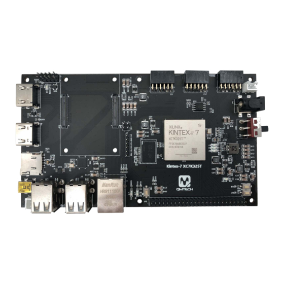
QMTECH XC7K325T DEV BOARD
USER MANUAL
Preface
The QMTECH® XC7K325T development board uses Xilinx Kintex®-7 devices to demonstrate best price/
performance/watt at 28nm while giving you high DSP ratios, cost-effective packaging, and support for
mainstream standards like PCIe® Gen3 and 10 Gigabit Ethernet. The Kintex-7 family is ideal for applications
including 3G and 4G wireless, flat panel displays, and video over IP solutions.
QMTECH XC7K325T Development Board
User Manual V01
Advertisement

Subscribe to Our Youtube Channel
Related Manuals for QMTECH XC7K325T


Summary of Contents for QMTECH XC7K325T
- Page 1 USER MANUAL Preface The QMTECH® XC7K325T development board uses Xilinx Kintex®-7 devices to demonstrate best price/ performance/watt at 28nm while giving you high DSP ratios, cost-effective packaging, and support for mainstream standards like PCIe® Gen3 and 10 Gigabit Ethernet. The Kintex-7 family is ideal for applications including 3G and 4G wireless, flat panel displays, and video over IP solutions.
-
Page 2: Table Of Contents
..................3 VERVIEW 2. GETTING STARTED ..................4 2.1 I ..............5 NSTALL EVELOPMENT OOLS 2.2 QMTECH XC7K325T D ..... 6 EVELOPMENT OARD ARDWARE ESIGN 2.2.1 FPGA Power Supply ............6 2.2.1 FPGA 1.0V Core Power Supply ........7 2.2.2 System Clock ..............7 2.2.3 SPI Flash Boot .............. -
Page 3: Introduction
On-Board core power supply for FPGA by using MP8712 wide input range DC/DC, it can provide 12A continuous/15A peak output current; XC7K325T development board has one 50p, 2.54mm pitch headers for extending user IOs. All IOs are precisely designed with length matching; XC7K325T development board has 3 user switches;... -
Page 4: Getting Started
Getting Started Below image shows the dimension of the QMTECH XC7K325T development board: 160mm x 90mm. The unit in below image is millimeter(mm). Figure 2-1. QMTECH XC7K325T Development Board Dimension QMTECH XC7K325T Development Board User Manual V01... -
Page 5: Install Development Tools
Install Development Tools To develop FPGA applications, users need to prepare Xilinx Vivado 2018.3, Xilinx USB platform cable, XC7K325T development board and 6V DC power supply. Below image shows the Xilinx Vivado 2018.3 development environment which could be downloaded from... -
Page 6: Qmtech Xc7K325T Development Board Hardware Design
QMTECH XC7K325T Development Board Hardware Design 2.2.1 FPGA Power Supply The development board needs DC input as power supply which could be directly injected from power header JP1. The on board LED D4 indicates the 3.3V supply status, it will be turned on when the power supply is active. -
Page 7: Fpga 1.0V Core Power Supply
Figure 2-5. 50MHz System Clock 2.2.3 SPI Flash Boot In default, the FPGA XC7K325T boots from external SPI Flash, detailed hardware design is shown in below figure. The SPI flash is using S25FL128L manufactured by Infineon(Spansion), with 128Mbit memory storage. S25FL128L FPGA_CSO_B 4.7K... - Page 8 The LED D1 will be turned on after the FPGA successfully loading configuration file from SPI Flash during power on stage. In this case, LED D1 could be used as FPGA loading status indicator. FPGA_DONE Figure 2-8. FPGA_DONE Status Indicator QMTECH XC7K325T Development Board User Manual V01...
-
Page 9: User Extension Ios
The on board JTAG port uses 6P 2.54mm pitch header which could be easily connected to Xilinx USB platform cable. Below image shows the hardware design of the JTAG port: JTAG Figure 2-10. JTAG Port QMTECH XC7K325T Development Board User Manual V01... -
Page 10: User Leds
Below image shows three user LEDs: R286 LED4 LED2 LED3 Figure 2-11. User LEDs Below table shows the connection between XC7K325T and user LEDs. Number LED Name XC7K325T Pin Number 2.2.7 User Keys Below image shows the PROGRAM_B key and two user keys: 4.7k... -
Page 11: Ddr3 Memory
VSS8 VDDQ6 VSS9 VDDQ7 VSS10 VDDQ8 VSS11 VDDQ9 VSS12 VSSQ1 VSSQ2 VSSQ3 1K 1% VSSQ4 VSSQ5 DDR_VREF VSSQ6 VSSQ7 DDR_VREF VREFCA VSSQ8 1K 1% VSSQ9 DDR_VREF VREFDQ MT41K128M16JT-125:K 240R 1% Figure 2-13. DDR3 QMTECH XC7K325T Development Board User Manual V01... -
Page 12: Gpios Connected To Computer Module
The development board contains many of the interfaces for the Raspberry Pi CM4. Such as HDMI display port, ethernet interface, USB hub, TF card slot, etc. Below image shows the example setup for the XC7K325T development board and RPi CM4 module. Notifications: (1). - Page 13 The GPIOs are used for the communication between XC7K325T and RPi CM4 module. Users may also configure the GPIOs into Secondary mem Address bus at RPi CM4 side to get faster communication speed. Below table shows the connection between XC7K325T and GPIOs.
-
Page 14: Reference
Reference [1] ug470_7Series_Config.pdf [2] ds182_Kintex_7_Data_Sheet.pdf [3] ug475_7Series_Pkg_Pinout.pdf [4] S25FL128L_S25FL128L_256-MB_32-MB_128-MB_16-MB_3.0_V_FL-L_FLASH_MEMORY.pdf [5] MT41K128M16.pdf [6] TPS563201.pdf [7] MP8712.PDF QMTECH XC7K325T Development Board User Manual V01... -
Page 15: Revision
Revision Doc. Rev. Date Comments 01/12/2024 Initial Version. 25/03/2024 V1.0 Formal Release. QMTECH XC7K325T Development Board User Manual V01...
Need help?
Do you have a question about the XC7K325T and is the answer not in the manual?
Questions and answers