Table of Contents
Advertisement
Quick Links
Note: Please refer to the original service manual for:
DVD Mechanism Unit, Order No. PSG1012001CE
Speaker system SB-XH60GS-K (SA-XH60GA/GAX ), Order No. PSG1303032CE
Speaker system SB-XH100GW-K (SA-XH100GA/GAX), Order No. PSG1301009CE
Speaker system SB-XH160GS-K (SA-XH160GA/GAX), Order No. PSG1304042CE
TABLE OF CONTENTS
1 Safety Precautions----------------------------------------------- 3
1.1. General Guidelines---------------------------------------- 3
1.2. Before Repair and Adjustment ------------------------- 4
1.3. Protection Circuitry ---------------------------------------- 4
1.4. Caution For Fuse Replacement------------------------ 4
1.5. Safety Part Information----------------------------------- 4
2 Warning -------------------------------------------------------------- 5
to Electrostatically Sensitive (ES) Devices---------- 5
2.2. Precaution of Laser Diode------------------------------- 6
2.4. Handling Precautions for Traverse Unit-------------- 8
DVD Home Theater Sound System
Model No.
Product Color: (K)...Black Type
PAGE
3 Service Navigation --------------------------------------------- 10
3.1. Service Information -------------------------------------- 10
4 Specifications ---------------------------------------------------- 11
4.1. Others (Licenses) --------------------------------------- 12
5 General/Introduction------------------------------------------- 13
5.1. Power-Saving Features -------------------------------- 13
5.3. Disc Information ------------------------------------------ 15
6 Location of Controls and Components------------------ 17
6.1. Remote Control Key Button Operations------------ 17
6.2. Main Unit Key Button Operations -------------------- 18
© Panasonic Corporation 2013. All rights reserved.
Unauthorized copying and distribution is a violation
of law.
SA-XH60GA
SA-XH60GAX
SA-XH100GA
SA-XH100GAX
SA-XH160GA
SA-XH160GAX
PSG1304013CE
PAGE
Advertisement
Table of Contents
Troubleshooting

Related Manuals for Panasonic SA-XH60GA


Summary of Contents for Panasonic SA-XH60GA
-
Page 1: Table Of Contents
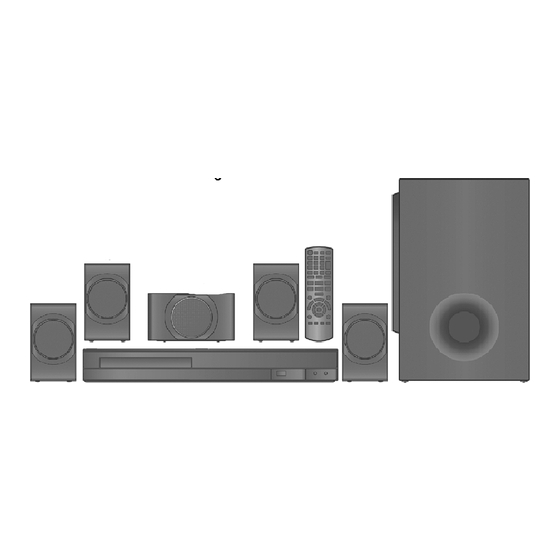
Product Color: (K)...Black Type Note: Please refer to the original service manual for: DVD Mechanism Unit, Order No. PSG1012001CE Speaker system SB-XH60GS-K (SA-XH60GA/GAX ), Order No. PSG1303032CE Speaker system SB-XH100GW-K (SA-XH100GA/GAX), Order No. PSG1301009CE Speaker system SB-XH160GS-K (SA-XH160GA/GAX), Order No. PSG1304042CE... - Page 2 7 Installation Instructions--------------------------------------- 19 19.1. Exploded View and Mechanical Replacement 7.1. Speaker Connections ----------------------------------- 19 Parts List -------------------------------------------------- 107 7.2. Radio antenna connection ----------------------------- 20 19.2. Electrical Replacement Parts List ------------------ 113 7.3. Connection with an ARC compatible TV ----------- 21 8 Operating Instructions ---------------------------------------- 22 8.1.
-
Page 3: Safety Precautions
1 Safety Precautions 1.1. General Guidelines 1. IMPORTANT SAFETY NOTICE There are special components used in this equipment which are important for safety. These parts are marked by in the Schematic Diagrams, Circuit Board Layout, Exploded Views and Replacement Parts List. It is essential that these critical parts should be replaced with manufacturer’s specified parts to prevent X-RADIATION, shock, fire, or other hazards. -
Page 4: Before Repair And Adjustment
1.2. Before Repair and Adjustment Disconnect AC power to discharge unit AC Capacitors (C5702, C5703, C5704, C5705, C5706) through a 10 Ω, 10 W resistor to ground. Caution: DO NOT SHORT-CIRCUIT DIRECTLY (with a screwdriver blade, for instance), as this may destroy solid state devices. After repairs are completed, restore power gradually using a variac, to avoid overcurrent. -
Page 5: Warning
2 Warning 2.1. Prevention of Electrostatic Discharge (ESD) to Electrostatically Sensi- tive (ES) Devices Some semiconductor (solid state) devices can be damaged easily by static electricity. Such components commonly are called Elec- trostatically Sensitive (ES) Devices. The following techniques should be used to help reduce the incidence of component damage caused by electrostatic discharge (ESD). -
Page 6: Precaution Of Laser Diode
2.2. Precaution of Laser Diode Caution: This product utilizes a laser diode with the unit turned “on”, invisible laser radiation is emitted from the pickup lens. Wavelength: 655 nm (DVD)/790 nm (CD) Maximum output radiation power from pickup: 100 µW/VDE Laser radiation from the pickup unit is safety level, but be sure the followings: 1. -
Page 7: Service Caution Based On Legal Restrictions
2.3. Service caution based on Legal restrictions 2.3.1. General description about Lead Free Solder (PbF) The lead free solder has been used in the mounting process of all electrical components on the printed circuit boards used for this equipment in considering the globally environmental conservation. The normal solder is the alloy of tin (Sn) and lead (Pb). -
Page 8: Handling Precautions For Traverse Unit
2.4. Handling Precautions for Traverse Unit The laser diode in the optical pickup unit may break down due to static electricity of clothes or human body. Special care must be taken avoid caution to electrostatic breakdown when servicing and handling the laser diode in the traverse unit. Cautions to Be Taken in Handling the Optical Pickup Unit 2.4.1. -
Page 9: Grounding For Electrostatic Breakdown Prevention
Grounding for electrostatic breakdown prevention 2.4.2. Some devices such as the DVD player use the optical pickup (laser diode) and the optical pickup will be damaged by static electric- ity in the working environment. Proceed servicing works under the working environment where grounding works is completed. 2.4.2.1. -
Page 10: Service Navigation
3 Service Navigation 3.1. Service Information This service manual contains technical information which will allow service personnel’s to understand and service this model. Please place orders using the parts list and not the drawing reference numbers. If the circuit is changed or modified, this information will be followed by supplement service manual to be filed with original service manual. -
Page 11: Specifications
4 Specifications VIDEO SECTION Video system PAL, NTSC Main unit Composite video output GENERAL 1 Vp-p (75 Ω) Output level Power supply AC 220 V to 240 V, 50/60 Hz Terminal Pin jack (1 system) Power consumption 50 W HDMI AV output Dimensions (W×... -
Page 12: Others (Licenses)
4.1. Others (Licenses) -
Page 13: General/Introduction
5 General/Introduction 5.1. Power-Saving Features... -
Page 14: Linked Operations With The Tv (Viera Link "Hdavi Control™")
5.2. Linked Operations with the TV (VIERA Link “HDAVI Control™”) -
Page 15: Disc Information
5.3. Disc Information 5.3.1. Media that can be played... - Page 16 5.3.2. File Extension Type Support (MP3/JPEG/Xvid)
-
Page 17: Location Of Controls And Components
6 Location of Controls and Components 6.1. Remote Control Key Button Operations... -
Page 18: Main Unit Key Button Operations
6.2. Main Unit Key Button Operations... -
Page 19: Installation Instructions
7 Installation Instructions Turn off all equipment before connection and read the appropriate operating instructions. Do not connect the AC power supply cord until all other connections are completed. 7.1. Speaker Connections... -
Page 20: Radio Antenna Connection
7.2. Radio antenna connection... -
Page 21: Connection With An Arc Compatible Tv
7.3. Connection with an ARC compatible TV... -
Page 22: Operating Instructions
8 Operating Instructions 8.1. Removing of disc during abnormality 8.1.1. Using main unit key buttons. 8.1.1.1. When the power can be turned off. 1. Turn off the power and press & hold [OPEN/CLOSE] button on main unit and [SKIP FWD] button on remote for 5 seconds 8.1.1.2. - Page 23 3. Gently pull out the tray. Caution: If the tray is not able to move, do not use force to pull out. 4. Remove the disc Figure 8-2...
-
Page 24: Service Mode
9 Service Mode 9.1. Cold-Start Here is the procedures to carry out cold-start for initialize to shipping mode. 1. Unplug AC power cord 2. Press & hold [ ] button 3. Plug AC power cord while [ ] button being pressed FL Display will show “_ _ _ _ _ _ _ _”... - Page 25 Product Series Country Region Broadcasting Selected Region Display Code OSD Menu Language Code System TV System (Default) Default USA, Canada, English (NA), Spanish (NA), P, PC, PX, NTSC AUTO2 (*A) English US Military Canadian French (blank) Japan NTSC AUTO2 (*A) Japanese Japanese, English English (EU), French, German,...
- Page 26 9.2.2. Setting of Panel Code This section describes the procedure necessary after replacement with a new Main P.C.B. (Refer to Section 17.2 for the assigned Main P.C.B. part number). Step 1 Press [OPEN/CLOSE] button on main unit, follow by [4] and [7] on remote control (to enter Doctor Mode). Step 2 Press [CANCEL] button on remote control, then press [2], [2], [8] and [0] on remote control.
-
Page 27: Self Diagnostic
9.3. Self Diagnostic By pressing various button combinations on the main unit and remote control unit, you can activate the various service modes for checking. Special Note: • Due to the limitations of the no. characters that can be shown on the FL Display, the “FL Display” button on the remote control unit can be used to show the two display pages. - Page 28 9.3.2. Self Diagnostic Table 2 (For DVD) Item Key Operation FL Display Mode Name Description Front Key DVD laser DVD laser drive current measurement. In STOP (no disc) mode, drive current For DVD laser drive current, refer to press [OPEN/CLOSE] measurement Troubleshooting Guide (Section 10.2) button on the main unit,...
- Page 29 9.3.3. Self Diagnostic Table 3 (For DVD) Item Key Operation FL Display Mode Name Description Front Key Micro-processor Micro-processor firmware version In STOP (no disc) (Display 1) firmware version display & EEPROM checksum display. mode, press display & EEPROM checksum is only available [OPEN/CLOSE] button on EEPROM due to existence of EEPROM IC.
- Page 30 9.3.4. Self Diagnostic Table 4 (For DVD) Item Key Operation FL Display Mode Name Description Front Key Region and DVD firmware version is displayed on In STOP (no disc) Firmware the FL Display. mode, press version display [OPEN/CLOSE] button on the main unit, and [8] button on the remote control unit.
-
Page 31: Self Diagnostic Table
9.3.5. Self Diagnostic Table 5 Item Key Operation FL Display Mode Name Description Front Key Press & hold Self-Diagnostic To enter into self-diagnostic checking [OPEN/CLOSE] on main Mode unit, follow by [4] then [9] on remote control. (When no disc in tray) Error code will display Error code System will perform a check on... -
Page 32: Error Code
9.4. Error Code 9.4.1. Error Code Table 1 Error Diagnosis Description of error Automatic FL Display Remarks Code Contents The abnormalities In normal operation, when DCDET2 goes to Press [OPEN/CLOSE] in the Power Amp L, immediately PCNT is set to L (not normal on main unit for next output or power POWER OFF sequence), and Error Code... - Page 33 9.4.2. Error Code Table 2 Error Diagnosis Description of error Automatic FL Display Remarks Code Contents The tray opening and closing is abnormal. Press [OPEN/CLOSE] on Tray loading error CLOSE and OPEN of the tray cannot be main unit for next error. carried out properly.
-
Page 34: Sales Demonstration Lock Function
9.5. Sales Demonstration Lock Function This function prevents discs from being lost when the unit is used for sales demonstrations by disabling the disc eject function. “LOCKED” is displayed on the unit, and ordinary operation is disabled. 9.5.1. Entering into Sales Demonstration Lock Function •... -
Page 35: Firmware Version-Up Information
9.6. Firmware Version-Up Information 9.6.1. Process Flow (1/2) Item FL/ GUI Display Remarks Process Description Collect ROM Step 1 Display 1: User can put both files Files Unzip the firmware update file. into the same root (Copy files into Step 2 directory. - Page 36 9.6.2. Process Flow (2/2) Item FL/ GUI Display Remarks Process Description To initialize, press and hold GUI Display 1.3: Update Completed main unit [OPEN/CLOSE] If firmware software update then press remote control completes successfully: key [ 10]. GUI Display 1.3: "Firmware update is completed, please open the tray and remove the disc."...
-
Page 37: Troubleshooting Guide
10 Troubleshooting Guide 10.1. Troubleshooting Guide for F61 and/or F76 This section illustrates the checking procedures when upon detecting the error of “F61” and/or “F76” after power up of the unit. It is for purpose of troubleshooting and checking in SMPS P.C.B.. Symptom(s) Possible Fault(s) Checking items... - Page 38 10.1.1. SMPS P.C.B. AC Inlet Jack : P5701 Regulator IC : Thermal Diode : Photocoupler : IC2900 D5706 PC701 Fuse : F1 Connector : H2016 H2016 Transformer : T5701 Figure 10-1 SMPS P.C.B.
- Page 39 10.1.2. Main P.C.B. (Side A of Main P.C.B.) Transistor:Q100 D114 Chip Jumper:K105 Chip Jumper:K304 Chip Jumper:K102 (Side B of Main P.C.B.) DC/DC CONVERTER IC: IC106 Inductors : L125 Connector:CN100 IC107 Transistor:Q107 Connector:CN203 Figure 10-2. Main P.C.B.
-
Page 40: Dvd/Cd Laser Diode Current Measurement
10.2. DVD/CD Laser Diode current measurement This section will illustrate proceddures of measuring & deriving DVD/CD Laser Diode Current. Item Description Checking Item/Formula Remarks 1. Measurement the voltage (V ) on the testpoints CL8530(+) & CL8531(-). Backend P.C.B. CD Laser Diode Current Measurement (Figure 10-3 This is voltage across R8566 which has a resistance value of 4.7 ohm. - Page 41 10.2.1. Backend P.C.B. (Side A of Backend P.C.B.) R8566 R8556 (Side B of Backend P.C.B.) CL8530, CL8531, CL8532 Figure 10-3 Backend P.C.B.
-
Page 42: Basic Troubleshooting Guide For Backend P.c.b
10.3. Basic Troubleshooting Guide for Backend P.C.B. Problems Checking Points Checking components 1) Distorted picture or a) Check SDRAM address, data IC8051 abnormal sound is head bus, CLK and other control signals during the initialization waveform b) Check video signals i) IC8001 Pin 61, 63, 65, 66 ii) L4002, L4003, L4004, L4005 iii) JK4001... -
Page 43: Basic Troubleshooting Guide For Hdmi Av Output
10.4. Basic Troubleshooting Guide for HDMI AV output Problems Checking Points Checking components 1) TV does not have any 1) Check setting of the set in * This year HDMI always ON. display. Set FL display shows Setup Menu whether the HDMI No need to check Setup Menu. -
Page 44: Service Fixture & Tools
11 Service Fixture & Tools Prepare service tools before process service position. Ref. No Service Tools Remarks SFT1 Main P.C.B. (CN201) - Backend P.C.B. (FP8101) RFKZ0500 (50P FFC) [SPG]... -
Page 45: Disassembly And Assembly Instructions
12 Disassembly and Assembly Instructions Caution Note: • This section describes the disassembly and/or assembly procedures for all major printed circuit boards & main compo- nents for the unit. (You may refer to the section of “Main components and P.C.B Locations” as described in the service manual) •... -
Page 46: Disassembly Flow Chart
12.2. Disassembly Flow Chart Main Unit 12.4. Top Cabinet 12.5. Tray Ornament 12.12. DVD Mechanism 12.8. Rear Panel 12.6. Front Panel Block Unit 12.7. Panel P.C.B. and 12.9. SMPS P.C.B. 12.13. Traverse Unit Power Button P.C.B. 12.10. Main P.C.B. 12.11. Backend P.C.B. -
Page 47: Main Components And P.c.b. Locations
12.3. Main Components and P.C.B. Locations... -
Page 48: Disassembly Of Top Cabinet
12.4. Disassembly of Top Cabinet Step 4 Slightly lift both sides of the Top Cabinet in an outward direction about 30°. Step 1 Remove 2 screws. Step 2 Remove 3 screws. Step 5 Press to release and remove the Top Cabinet as arrow shown in sequence. -
Page 49: Replacement Of Tray Ornament
Caution: During assembling, ensure that the Top Cabinet Step 3 Slide the Tray out as direction of arrow. is inserted into the Front Panel Block. Caution: Do not use strong forces. 12.5. Replacement of Tray Ornament 12.5.1. Disassembly of Tray Ornament Step 4 Upset the Unit. -
Page 50: Disassembly Of Front Panel Block
12.5.2. Assembly of Tray Ornament 12.6. Disassembly of Front Panel Step 1 Align the guide rib of Tray Ornament with the Tray. Block Step 2 Insert the Tray Ornament into the Tray. • Refer to “Disassembly of Top Cabinet”. Caution: Ensure that the Tray Ornament is fully catched •... -
Page 51: Disassembly Of Panel P.c.b. And Power Button P.c.b
Step 6 Release tabs at the bottom of the unit. Step 7 Remove the Front Panel Block. Caution: Do not exert strong force when releasing the tabs. 12.7. Disassembly of Panel P.C.B. and Power Button P.C.B. • Refer to “Disassembly of Top Cabinet”. •... - Page 52 Step 3 Lift up to remove the Panel P.C.B.. Caution: During assembling, dressed the 5P wire & 17P FFC are dressed as diagram shown. Caution: During assembling, ensure that the Panel P.C.B. is properly located and fully seated onto the Front Panel Block.
-
Page 53: Disassembly Of Rear Panel
Caution: During assembling, ensure that the Power Button 12.8. Disassembly of Rear Panel P.C.B. is located properly and fully seated onto the Front • Refer to “Disassembly of Top Cabinet” Panel Block. Step 1 Remove 7 screws. Step 7 Release the 3P Cable from the ribs of the Front Panel Step 2 Release tabs on each side of the Rear Panel in the Block. -
Page 54: Disassembly Of Smps P.c.b
12.9. Disassembly of SMPS P.C.B. Step 3 Remove 4 screws. • Refer to “Disassembly of Top Cabinet”. Step 1 Remove 1 screw. Step 4 Lift up to remove the SMPS P.C.B.. Caution: Handle the SMPS P.C.B. with care. Avoid touching the heatsink due to its prolong use. -
Page 55: Disassembly Of Main P.c.b
Caution: Replace the Bottom PC Sheet if broken. Ensure Step 3 Detach 12P Cable at the connector (CN100) on Main that it is pasted on the Bottom Chassis properly. P.C.B.. Step 4 Detach 17P FFC at the connector (CN203) on Main P.C.B.. -
Page 56: Disassembly Of Backend P.c.b
Step 7 Slightly lift up to remove the Main P.C.B.. 12.11. Disassembly of Backend P.C.B. • Refer to “Disassembly of Top Cabinet”. Step 1 Remove 7 screws. Step 2 Release tabs at each side of the Rear Panel in the direction of arrow. -
Page 57: Disassembly Of Dvd Mechanism Unit
Step 8 Remove 2 screws. 12.12. Disassembly of DVD Mecha- nism Unit • Refer to “Disassembly of Top Cabinet” • Refer to “Replacement of Tray Ornament” Step 1 Detach 24P FFC at the connector (FP8531) on Backend P.C.B.. Step 2 Detach 6P FFC at the connector (FP8251) on Backend P.C.B.. -
Page 58: Replacement Of Traverse Unit
Step 5 Slightly lift up to remove the DVD Mechanism Unit. 12.13. Replacement of Traverse unit Caution: During assembling, ensure that the DVD Mecha- • Refer to “Disassembly of DVD Mechanism Unit”. nism Unit is properly inserted & fully seated on the bottom Caution: Refer to 2.4 “Handling Precaution for Traverse chasiss before screwing. - Page 59 Step 2 : Slide the tray out fully. Step 4 : Release the guide as shown & slide the Traverse Slide Plate to the end. Step 3 : Release the catches & remove the tray. Step 5 : Remove the Tesa Tape. Caution: During Assembling, ensure use new Tesa Tape for pasting.
- Page 60 Step 7 : Lift the Traverse Unit by approximately 45 degree. 12.13.2. Assembly of Traverse Unit Step 8 : Slide out the Traverse Unit as arrow shown. Step 1 : Release the guide as shown & slide again the Traverse Slide Plate to the end. Caution : Avoid touching the surface of the OPU in the Traverse Unit.
- Page 61 Step 2 :Slot the Traverse unit at approximately 45°. into the Step 3 Ensure the Traverse Unit seated properly onto the mecha chassis as arrow shown. Groove.
- Page 62 Step 4 Slide Traverse Slide Plate to lock the Traverse Unit as Step 6 Paste the Tesa Tape as shown and press the Tesa Tape shown. to ensure that Tesa Tape fully tape. Caution : Ensure use new Tesa Tape only for pasting. Step 5 Slot the FFC onto the slot and pull out a little bit to ensure FFC cable is strain.
- Page 63 Step 7 Release the guide as shown & slide again the Traverse Step 9 Ensure the guides is align with the groove when sliding Slide Plate to the end. the tray in. Step 10 Slide the tray in fully. Step 8 Slot in the Tray into the guides as Picture shown.
-
Page 64: Service Position
13 Service Position Note: For description of the disassembly procedures, see 13.2. Checking of SMPS P.C.B. the Section 12. Step 1 Remove Top Cabinet. 13.1. Checking of Panel P.C.B. Step 2 Remove SMPS P.C.B.. Step 3 Place the SMPS P.C.B. on the insulated material. Step 1 Remove Top Cabinet. -
Page 65: Checking Main P.c.b
13.3. Checking Main P.C.B. Step 6 Upset Main P.C.B. and place it onto the insulated mate- rial. 13.3.1. Checking Main P.C.B. (Side A) Step 7 Proceed to check side A of Main P.C.B.. Step 1 Remove Top Cabinet. Step 2 Remove Main P.C.B.. Step 3 Connect 12P Cable at the connector (CN100) on Main P.C.B.. -
Page 66: Checking Backend P.c.b
Step 4 Lift up to remove the Main P.C.B.. Step 5 Place the Main P.C.B. as shown. Step 6 Connect 12P Cable at the connector (CN100) on Main P.C.B.. Step 7 Connect 17P FFC at the connector (CN203) on Main P.C.B.. - Page 67 13.4.2. Checking of Backend P.C.B. (Side Step 5 Upset Backend P.C.B. and place it onto insulated mate- rial as diagram shown. Step 6 Proceed to check Side A of Backend P.C.B.. Step 1 Remove Top Cabinet. Step 2 Remove 7 screws. Step 3 Release tabs at each side of the Rear Panel in the direction of arrow.
-
Page 69: Block Diagram
9 VOTR- FROM/TO SYSTEM CONTROL FP8252 CLOSE SW CLOSE SW FP8101 CN201 CLOSE SW CLOSE SW FP8252 FP8101 CN201 OPEN SW OPEN SW OPEN SW OPEN SW NOTE: “ * ” REF IS FOR INDICATION ONLY SA-XH60GA/GAX,SA-XH100GA/GAX,SA-XH160GA/GAX BACKEND BLOCK DIAGRAM... -
Page 70: Ic Terminal Chart
CN203 CN901 KEY1 KEY1 H902 H901 KEY1 KEY1 90 FROM/TO SYNC SYNC SYNC POWER SUPPLY Z901 DC DET1 REMOTE CONTROL DC DET1 DCDET1 SENSOR USB OC CN203 CN901 USB OC USB OC RMT 3 3.3V SA-XH60GA/GAX,SA-XH100GA/GAX,SA-XH160GA/GAX SYSTEM CONTROL BLOCK DIAGRAM... -
Page 71: System Control
BST D VALID JK401 VALID 7 RST AB OUT D SUBWOOFER JK401 17 RST CD OUT C BST C DC DET2 DC DETECT DC DET2 23.5V CIRCUIT Q114,Q116,Q500,Q501 FROM DC DET2 DC DET2 POWER SUPPLY SA-XH60GA/GAX,SA-XH100GA/GAX,SA-XH160GA/GAX AUDIO & VIDEO BLOCK DIAGRAM... -
Page 72: Audio And Video
Q5841 D402 DC DETECT DC DET2 DC DET2 AUDIO & VIDEO DZ5701 TH5702 D110 D111 D112 D115 Q105 Q106 PRIMARY SECONDARY DC DETECT DC DETECT NOTE: “ * ” REF IS FOR INDICATION ONLY SA-XH60GA/GAX,SA-XH100GA/GAX,SA-XH160GA/GAX POWER SUPPLY (1/2) BLOCK DIAGRAM... - Page 73 VREF PW 3.3VREF 3.3V PW FL- CN203 CN901 CN203 CN901 PW FL+ CN203 CN901 PW -VP PW 3.3V D 3.3V CN203 CN901 3.3V 3.3V 3.3V NOTE: “ * ” REF IS FOR INDICATION ONLY SA-XH60GA/GAX,SA-XH100GA/GAX,SA-XH160GA/GAX POWER SUPPLY (2/2) BLOCK DIAGRAM...
-
Page 74: Wiring Connection Diagram
TO uP DOWNLOADER (SIDE B) AC IN SMPS P.C.B. T2900 SURROUND 220V-240V SWITCHING (SOLDER SIDE) 50Hz TRANSFORMER CN100 7 6 5 4 FRONT H2016* SPEAKERS CENTER SUBWOOFER NOTE: " * " REF IS FOR INDICATION ONLY. SA-XH60GA/GAX,SA-XH100GA/GAX,SA-XH160GA/GAX WIRING CONNECTION DIAGRAM... -
Page 75: Schematic Diagram
16 Schematic Diagram 16.1. Schematic Diagram Notes • Voltage and signal line : +B signal line • This schematic diagram may be modified at any time : -B signal line with the development of new technology. : Audio output signal line Notes: : Video output signal line S901:... -
Page 77: Backend Circuit
PW_USB_5V C9006 K8005 K8010 K8001 K8006 D8301 DA3X101F0L R8324 R8323 R8321 R8322 JK8301 VGND VGND R8325 C2823 L2802 R8326 LB8317 VIDEO OUT 100P J0JBC0000015 VIDEO (YEL) TO BACKEND CIRCUIT (2/6) R9082 PW_D+3R3V CL9802 TO BACKEND CIRCUIT (4/6) SA-XH60GA/GAX,SA-XH100GA/GAX,SA-XH160GA/GAX BACKEND CIRCUIT... - Page 78 UART_RX C8051 OPEN_SW OPEN SW CLOSE_SW CLOSE_SW VBUS_EN IC8051 VBUS_EN USB_OC C8055 C3ABPY000070 USB_OC AMUTE 64M SDRAM AMUTE ADGND MIC_IN MIC_IN VGND VGND iPod_VIDEO iPod_SW TO BACKEND TO BACKEND CIRCUIT (1/6) CIRCUIT (3/6) TO BACKEND CIRCUIT (5/6) SA-XH60GA/GAX,SA-XH100GA/GAX,SA-XH160GA/GAX BACKEND CIRCUIT...
- Page 79 220K H0J270500131 K8301 R8311 C8621 1000P L8302 G1C100M00049 C8006 100P C8029 1000P LB3902 TO BACKEND J0JHC0000045 C8028 0.01 CIRCUIT (2/6) PW_VDDP_HDMI LB3901 J0JHC0000045 PW_DAC LB8301 J0JHC0000045 C3902 C3901 C8301 6.3V100 6.3V100 6.3V100 TO BACKEND SA-XH60GA/GAX,SA-XH100GA/GAX, CIRCUIT (6/6) SA-XH160GA/GAX BACKEND CIRCUIT...
- Page 80 FOR FIRMWARE +3.3V VOLTAGE REGULATOR +1.8V VOLTAGE SUPPLY REGULATOR DUPRDO DOWNLOAD DGND DGND 1.8V R8103 C8113 FP8002 C8101 VDD_3R3V DUPTDI R8104 DUPTDI FOR FIRMWARE DUPRDI DUPRDI R8101 DEBUG 270K DGND DOWNLOAD DOWNLOAD C8112 C8111 R8102 130K DGND SA-XH60GA/GAX,SA-XH100GA/GAX,SA-XH160GA/GAX BACKEND CIRCUIT...
- Page 81 RFIN_P D1H45602A014 R8542 RF_A RX8532 RF_B D1H45602A014 RF_F R8537 PD GND TO OPTICAL PICKUP UNIT VC(REF) (DVD MECHANISM UNIT BRS1D) LB8531 C8533 RF_E R8538 DVD_MD R8531 VR-CD LB8561 R8532 VR-DVD J0JDC0000102 CD-LD LB8551 J0JDC0000102 DVD-LD GND-LD CD_MD SA-XH60GA/GAX,SA-XH100GA/GAX,SA-XH160GA/GAX BACKEND CIRCUIT...
- Page 82 CLK- R3905 CLKGND HDMI AV OUT CLK+ CLK+ (ARC) D0GND D1GND C3968 D2GND C3971 K3901 FRAME G3 G4 K3902 R3955 R3958 K3903 LB3909 J0JHC0000045 C3972 R3959 R3956 C3970 C3967 IC3953 R3900 100K GPIO34 R3957 C0JBAB000986 DUAL INVERTER SA-XH60GA/GAX,SA-XH100GA/GAX,SA-XH160GA/GAX BACKEND CIRCUIT...
-
Page 83: Main Circuit
AGND CN202 PW_3.3VREF VREF BUSY BUSY CLOCK CLOCK LB200 TO uP DOWNLOADER LB201 C214 VOUT 0.47 SYS5VGND DGND RESET PW_SYS6V CNVSS CNVSS STBY IC202 C205 0.47 C0DBGYY02930 +3.3V VOLTAGE REGULATOR RESET C219 0.01 TO MAIN CIRCUIT (5/8) SA-XH60GA/GAX,SA-XH100GA/GAX,SA-XH160GA/GAX MAIN CIRCUIT... - Page 84 C411 C401 OPEN_SW R400 OPEN SW CLOSE_SW CLOSE_SW VBUS_EN C453 VBUS_EN 0.01 USB_OC USB_OC AMUTE AMUTE ADGND C451 K105 MIC_IN C452 L427 VGND VGND J0JBC0000014 R435 iPod_VIDEO iPod_SW K158 TO MAIN CIRCUIT (3/8) TO MAIN CIRCUIT (6/8) SA-XH60GA/GAX,SA-XH100GA/GAX,SA-XH160GA/GAX MAIN CIRCUIT...
- Page 85 R233 DVD_TX DVD_RX R222 RX201 150K D1H81014A024 CNVSS R201 FLD_STB CLOSE_SW CK_FLD ECO_CNTRL FLD_OUT R232 SYNC RESET TUN_INT TUN_SCLK X201 H2D500400006 TUN_SDIO TUN_REST LED_CTRL R294 R239 R223 TO MAIN 5.6K CIRCUIT (2/8) TO MAIN SA-XH60GA/GAX,SA-XH100GA/GAX, CIRCUIT (7/8) SA-XH160GA/GAX MAIN CIRCUIT...
- Page 86 C509 0.01 PWM_D PVDD_D C519 PVDD_D 25V330 C455 L409 0.01 G0A100H00018 C510 0.033 SP_FR+ R452 BST_D R506 R453 GVDD_C GVDD_D SP_SL- C190 1000P C433 C432 C431 C567 C514 1000P K157 R454 CHASSIS TO MAIN SA-XH60GA/GAX,SA-XH100GA/GAX, CIRCUIT (8/8) SA-XH160GA/GAX MAIN CIRCUIT...
- Page 87 C309 680P TV_R R311 C312 TUN-LCH R307 C313 R309 R310 TUN-RCH R308 C314 OUT OF BOARD IC300 C0JBAR000367 AUDIO SELECTOR C315 C317 C316 R317 Q301 B1GBCFJJ0041 R315 SELECTOR SWITCH R312 R313 R318 R316 Q300 B1GBCFJJ0041 SELECTOR SWITCH SA-XH60GA/GAX,SA-XH100GA/GAX,SA-XH160GA/GAX MAIN CIRCUIT...
- Page 88 FL_IC_DAT (CN901) R702 CK_FLD R136 PW_SW5V_ADC FL_IC_CLK IN SCHEMATIC FLD_STB R137 FL_IC_STB DIAGRAM - 15 LB704 LED_CTRL G1C100M00049 LED_CTRL KEY1 KEY1 C708 KEY2 KEY2 6.3V47 PW_FL+ R139 PW_FL- R141 PW_-VP R142 TO MAIN CIRCUIT (7/8) LB703 J0JCC0000388 SA-XH60GA/GAX,SA-XH100GA/GAX,SA-XH160GA/GAX MAIN CIRCUIT...
- Page 89 D203 B1ABCF000231 G0A330G00016 DZ2J07500L DC DETECT Q100 C135 R152 0.01 B1DGDC000002 C198 R150 C142 C138 C141 C143 C129 SWITCH 25V4.7 0.47 25V470 SYS5VGND K107 D116 K104 Q101 B0JCPG000028 PW_SW5V_D K106 B1GBCFJJ0041 PCONT SWITCH PW_SW5V_ADC K102 R196 K101 SA-XH60GA/GAX,SA-XH100GA/GAX,SA-XH160GA/GAX MAIN CIRCUIT...
- Page 90 PVDD_D C554 25V330 PVDD_D L405 G0A100H00018 SP_SR+ R461 C550 0.033 BST_D PW_+12V R462 GVDD_C GVDD_D C439 C437 C438 C551 C441 K303 16V33 PW_PVDD_D R463 C802 C803 C512 HEATSINK* NOTE: “ * ” REF IS FOR INDICATION ONLY SA-XH60GA/GAX,SA-XH100GA/GAX,SA-XH160GA/GAX MAIN CIRCUIT...
-
Page 91: Panel And Power Button Circuit
USB PORT DGND 3 D+ IN SCHEMATIC R950 DGND DIAGRAM - 1 DGND R951 LB950 R952 POWER BUTTON CIRCUIT CHASSIS H901 S902 POWER DGND KEY1 VREF_LED SA-XH60GA/GAX,SA-XH100GA/GAX,SA-XH160GA/GAX PANEL / POWER BUTTON CIRCUIT NOTE: “ * ” REF IS FOR INDICATION ONLY... -
Page 92: Smps Circuit
R2908 C5725 C2912 DZ2J36000L D2906 16V33 16V820 25V100 6.3V100 B0EAMM000057 R5735 C5727 C5726 1000P 0.33 R5731 R5729 TO SMPS R5730 CIRCUIT (2/2) 4.7K IC5702 C0DBZMC00006 SHUNT REGULATOR R5817 NOTE: “ * ” REF IS FOR INDICATION ONLY SA-XH60GA/GAX,SA-XH100GA/GAX,SA-XH160GA/GAX SMPS CIRCUIT... - Page 93 R5728 CTRL D5704 B0JCME000035 C5719 0.22 OPTMR R5724 180K C5720 C5715 0.01 IC5701 C0DBZYY00448 SWITCHING MODE POWER SUPPLY CONTROL TO SMPS CIRCUIT (1/2) D5705 TH5701 R5723 B0BC02700039 D4CC11040013 NOTE: “ * ” REF IS FOR INDICATION ONLY SA-XH60GA/GAX,SA-XH100GA/GAX,SA-XH160GA/GAX SMPS CIRCUIT...
-
Page 94: Printed Circuit Board
C8024 R8255 R8256 IC8111 R8253 R8254 D8101 L8251 C8252 D8102 L8252 R8259 FL8103 C9006 FL8101 R8260 FL8104 FP8252 IC9006 LB9002 FP9001 (TO LOADING PCB (DVD MECHANISM FP8101 UNIT BRS1D)) 0680C 0680C 0680C 0680C (SIDE A) (SIDE B) SA-XH60GA/GAX,SA-XH100GA/GAX,SA-XH160GA/GAX BACKEND P.C.B. -
Page 95: Main P.c.b
C214 C501 C189 C502 C132 R142 R530 C187 R195 C191 R157 R156 C197 Q100 C522 C523 C192 D114 C186 C198 Q101 C181 C182 C472 C183 C184 C129 C473 C185 C486 C135 K109 C512 0729B 0729B (SIDE A) SA-XH60GA/GAX,SA-XH100GA/GAX,SA-XH160GA/GAX MAIN P.C.B. - Page 96 R435 C424 C476 30 32 SUBWOOFER R469 C412 L418 R442 C411 1-SW+ R411 RX404 IC106 RX405 C410 C415 R404 R444 C479 X400 R443 C425 C505 C420 R445 C138 C413 L419 C441 L125 C143 0729B 0729B (SIDE B) SA-XH60GA/GAX,SA-XH100GA/GAX,SA-XH160GA/GAX MAIN P.C.B.
-
Page 97: Panel And Power Button P.c.b
(VOL-) R952 LB950 R924 W929 R951 CN951* D901 13 15 R913 R950 W933 CN901 SENSOR PORT POWER BUTTON P.C.B. (REP4765A) H901 0731BB 0731BB S902 (POWER) NOTE: " * " REF IS FOR INDICATION ONLY. SA-XH60GA/GAX,SA-XH100GA/GAX,SA-XH160GA/GAX PANEL / POWER BUTTON P.C.B. -
Page 98: Smps P.c.b
C2912 TRANSFORMER) Q2900 R5702 T5701 W1039 C5705 W1033 (TRANSFORMER) H2016* R5704 R5703 0730B 0730B CAUTION RISK OF ELECTRIC SHOCK AC VOLTAGE LINE. PLEASE DO NOT TOUCH THIS P.C.B NOTE: " * " REF IS FOR INDICATION ONLY. SA-XH60GA/GAX,SA-XH100GA/GAX,SA-XH160GA/GAX SMPS P.C.B. -
Page 99: Appendix Information Of Schematic Diagram
STANDBY IC8001 REF NO. MODE HDMI STANDBY IC8001 REF NO. MODE HDMI STANDBY REF NO. IC8001 MODE HDMI STANDBY IC8001 REF NO. MODE HDMI STANDBY IC8001 REF NO. MODE HDMI STANDBY IC8051 REF NO. MODE HDMI STANDBY SA-XH60GA/GAX,SA-XH100GA/GAX,SA-XH160GA/GAX BACKEND P.C.B. - Page 100 REF NO. MODE HDMI STANDBY REF NO. IC9006 MODE CD PLAY STANDBY Q3901 Q3902 Q3903 Q3904 Q8552 REF NO. MODE HDMI STANDBY SA-XH60GA/GAX,SA-XH100GA/GAX,SA-XH160GA/GAX BACKEND P.C.B. 18.1.3. Backend P.C.B. (3/3) Q8562 Q8565 REF NO. MODE CD PLAY STANDBY SA-XH60GA/GAX,SA-XH100GA/GAX,SA-XH160GA/GAX BACKEND P.C.B.
- Page 101 STANDBY IC200 REF NO. MODE POWER ON STANDBY IC200 REF NO. MODE POWER ON STANDBY REF NO. IC201 MODE POWER ON STANDBY IC202 REF NO. MODE POWER ON STANDBY IC300 REF NO. MODE SELECTOR -5.0 STANDBY -5.0 SA-XH60GA/GAX,SA-XH100GA/GAX,SA-XH160GA/GAX MAIN P.C.B.
- Page 102 10.1 20.3 10.2 10.2 20.3 10.1 10.1 20.3 STANDBY 12.0 12.0 12.0 10.1 20.3 20.3 10.1 10.1 20.3 10.2 10.2 20.3 10.1 10.1 20.3 IC404 REF NO. MODE CD PLAY 20.3 10.2 12.0 STANDBY 20.3 10.2 12.0 SA-XH60GA/GAX,SA-XH100GA/GAX,SA-XH160GA/GAX MAIN P.C.B.
- Page 103 Q116 Q500 REF NO. MODE POWER ON 11.5 23.5 20.0 10.0 20.0 STANDBY 12.2 10.1 23.0 20.0 10.0 20.0 Q501 REF NO. MODE POWER ON 20.0 10.0 STANDBY 20.0 10.0 REF NO. Q300 Q301 MODE SELECTOR STANDBY SA-XH60GA/GAX,SA-XH100GA/GAX,SA-XH160GA/GAX MAIN P.C.B.
- Page 104 -24.9 -24.9 -24.9 -24.9 -24.9 -24.9 -24.9 -13.3 -25.0 -25.5 -11.1 -25.1 -22.9 -22.9 -22.9 -22.9 -22.9 -22.9 -22.9 -22.9 IC901 REF NO. MODE POWER ON -22.9 -22.8 STANDBY -22.9 -22.8 SA-XH60GA/GAX,SA-XH100GA/GAX,SA-XH160GA/GAX PANEL P.C.B. 18.1.8. SMPS P.C.B. IC2900 REF NO. MODE POWER ON 23.5 12.2 STANDBY 23.5 12.2...
-
Page 105: Waveform Table
18.1.9. Waveform Table 1.5Vp-p(50nsec/div) 2Vp-p(50nsec/div) 2Vp-p(20nsec/div) 1Vp-p(20nsec/div) 3.2Vp-p(500nsec/div) 3.6Vp-p(500nsec/div) 3.2Vp-p(1usec/div) 3.2Vp-p(1usec/div) 3.2Vp-p(500nsec/div) 1.4Vp-p(1usec/div) 12Vp-p(1usec/div) 1.4Vp-p(1usec/div) 1.4Vp-p(1usec/div) 12Vp-p(1usec/div) 4.8Vp-p(2usec/div) 12Vp-p(1usec/div) 1.25Vp-p(50usec/div) 5Vp-p(1usec/div) 2Vp-p(20nsec/div) -
Page 107: Exploded View And Replacement Parts List
(MAIN P.C.B.) *CN951 EXT A *H2016 CN203 CN950 (POWER BUTTON P.C.B.) (PANEL P.C.B.) CN100 CN202 (SMPS P.C.B.) T2900 ZJ5701 FL901 H901 SA-XH60GA-K/GAXK, SA-XH100GA-K/GAXK, SA-XH160GA-K/GAXK CABINET DRAWINGS NOTE: " * " PART IS NOT SUPPLIED / REF IS FOR INDICATION ONLY. - Page 108 19.1.2. Packaging ACCESSORIES BAG A1-1 AC CORD AC CORD SA-XH60GA/GAX OI BOOK FM INDOOR ANTENNA HDMI CABLE SB-XH60GS VIDEO CABLE F R O N T POLYFOAM (LEFT) POLYFOAM (RIGHT) SC-XH60GA-K/GAXK PACKAGING DRAWINGS...
- Page 109 ACCESSORIES BAG A1-1 AC CORD AC CORD SA-XH100GA/GAX OI BOOK FM INDOOR ANTENNA SB-XH100GW HDMI CABLE VIDEO CABLE F R O N T POLYFOAM (LEFT) POLYFOAM (RIGHT) SC-XH100GA-K/GAXK PACKAGING DRAWINGS...
- Page 110 ACCESSORIES BAG AC CORD A1-1 AC CORD SA-XH160GA/GAX OI BOOK **SPACER PAD FM INDOOR ANTENNA SB-XH160GS HDMI CABLE VIDEO CABLE F R O N T POLYFOAM (LEFT) POLYFOAM (RIGHT) SC-XH160GA-K/GAXK NOTE: "**" PARTS ARE NOT SUPPLIED. PACKAGING DRAWINGS...
-
Page 111: Mechanical Replacement Part List
19.1.3. Mechanical Replacement Part List Safety Ref. Part No. Part Name & Qty Remarks Description Safety Ref. Part No. Part Name & Qty Remarks RGUX1030-K VOLUME BUTTON Description RGUX1043-K OPEN/CLOSE BUT- CABINET RHD26043-1 SCREW CHASSIS RHD26046 SCREW RHD30007-K2J SCREW REE1778 (BACK- RHD30119-S SCREW... - Page 112 Safety Ref. Part No. Part Name & Qty Remarks Description RPG0E27 PACKING CASE XH60GA, XH60GAX RPG0D39 PACKING CASE XH100GA XH100GA RPG0D49 PACKING CASE XH160GA XH160GA RPN2533 POLYFOAM XH60GA, XH60GAX RPN2521 POLYFOAM XH100GA XH100GA RPN2374 POLYFOAM XH160GA XH160GA RPFX1010 MIRAMAT ACCESSORIES N2QAYB000853 REMOTE CONTROL A1-1...
-
Page 113: Electrical Replacement Parts List
19.2. Electrical Replacement Parts List Safety Ref. Part No. Part Name & Qty Remarks Description IC8001 C1AB00003476 (E.S.D) Safety Ref. Part No. Part Name & Qty Remarks IC8051 C3ABPY000070 (E.S.D) Description IC8111 C0DBEYY00215 (E.S.D) IC8112 C0DBEYY00175 (E.S.D) PRINTED CIRCUIT IC8251 C0GBY0000117 (E.S.D) BOARDS... - Page 114 Safety Ref. Part No. Part Name & Qty Remarks Safety Ref. Part No. Part Name & Qty Remarks Description Description L419 G0A100H00018 CHOKE COIL D101 DZ2J056M0L DIODE (E.S.D) L427 J0JBC0000014 INDUCTOR D110 DA2J10100L DIODE (E.S.D) L600 G1CR18JA0020 INDUCTOR D111 DA2J10100L DIODE (E.S.D) L2802...
- Page 115 Safety Ref. Part No. Part Name & Qty Remarks Safety Ref. Part No. Part Name & Qty Remarks Description Description REMOTE CONTROL W930 D0GBR00JA008 1/10W SENSOR W933 D0GBR00JA008 1/10W W940 D0GBR00JA008 1/10W Z901 B3RAB0000081 REMOTE CONTROL SENSOR RESISTORS THERMISTORS LB8531 D0GA220JA023 1/16W LB8691...
- Page 116 Safety Ref. Part No. Part Name & Qty Remarks Safety Ref. Part No. Part Name & Qty Remarks Description Description R291 D0GB104JA065 100K 1/10W R497 D0GB3R3JA065 1/10W R292 D0GB393JA065 1/10W R498 D0GB3R3JA065 1/10W R293 D0GB273JA065 1/10W R499 D0GB3R3JA065 1/10W R294 D0GB473JA065 1/10W R500...
- Page 117 Safety Ref. Part No. Part Name & Qty Remarks Safety Ref. Part No. Part Name & Qty Remarks Description Description R3903 D0GA103JA023 1/16W R8324 ERJ2RKD75R0X 1/16W R3904 D0GA472JA023 4.7K 1/16W R8325 D0GBR00J0004 1/10W R3905 D0GA202JA023 1/16W R8326 D0GBR00J0004 1/10W R3906 D0GA472JA023 4.7K 1/16W...
- Page 118 Safety Ref. Part No. Part Name & Qty Remarks Safety Ref. Part No. Part Name & Qty Remarks Description Description C143 F2A1E471B394 470uF C436 F1H1H104B055 0.1uF C150 F2A1C471B457 470uF C437 F1H1H104B055 0.1uF C151 F2A1C1010033 100uF C438 F1H1H104B055 0.1uF C158 F1H1H104B055 0.1uF C439 F1J1C106A059...
- Page 119 Safety Ref. Part No. Part Name & Qty Remarks Safety Ref. Part No. Part Name & Qty Remarks Description Description C600 F1H1H102B047 1000pF C5729 F1H1H103B047 0.01uF C601 F1H1H220A889 22pF C5843 F1H1C105A095 C602 F1H1H220A889 22pF C8001 EEE0GA331WP 330uF C603 F1H1A1050039 C8002 F1G1A1040006 0.1uF C604...
- Page 120 Safety Ref. Part No. Part Name & Qty Remarks Description FL8103 F1H0J1050018 6.3V FL8104 F1J1E1040022 0.1uF K8301 F1H1H102B047 1000pF SERVICE FIXTURE & TOOLS SFT1 RFKZ0500 (MAIN [SPG] P.C.B. TO BACK- END P.C.B.) MMH1304...
Need help?
Do you have a question about the SA-XH60GA and is the answer not in the manual?
Questions and answers