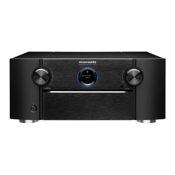
Marantz SR 8015 Service Manual
Av surround receiver
Hide thumbs
Also See for SR 8015:
- Quick start manual (14 pages) ,
- Owner's manual (351 pages) ,
- Quick start manual
Table of Contents
Advertisement
Quick Links
AV Surround Receiver
SR8015
• For purposes of improvement, specifications and design are subject to change without notice.
• Please use this service manual when referring to the operating instructions without fail.
• Some illustrations used in this service manual are slightly different from the actual product.
Service Manual
Click here!
On-line service parts list
https://dmedia.soundunited.com/documents/details/27246
ONLINE PARTS LIST
(P5)
WEB owner's manual
NA:
http://manuals.marantz.com/SR8015/NA/EN/index.php
EU:
http://manuals.marantz.com/SR8015/EU/EN/index.php
AP:
http://manuals.marantz.com/SR8015/AP/ZH/index.php
JP:
http://manuals.marantz.com/SR8015/JP/JA/index.php
Upload is planned for the time of a future press release.
BEFORE SERVICING THIS UNIT
ELECTRICAL
MECHANICAL
REPAIR INFORMATION
UPDATING
Please refer to the MODIFICATION NOTICE.
Confidential
Ver. 3
Advertisement
Table of Contents

Subscribe to Our Youtube Channel
Related Manuals for Marantz SR 8015


Summary of Contents for Marantz SR 8015
- Page 1 AV Surround Receiver SR8015 Click here! On-line service parts list https://dmedia.soundunited.com/documents/details/27246 ONLINE PARTS LIST (P5) WEB owner’s manual http://manuals.marantz.com/SR8015/NA/EN/index.php http://manuals.marantz.com/SR8015/EU/EN/index.php http://manuals.marantz.com/SR8015/AP/ZH/index.php http://manuals.marantz.com/SR8015/JP/JA/index.php Upload is planned for the time of a future press release. BEFORE SERVICING THIS UNIT ELECTRICAL MECHANICAL REPAIR INFORMATION UPDATING • For purposes of improvement, specifications and design are subject to change without notice.
- Page 2 BEFORE SERVICING THIS UNIT SAFETY PRECAUTIONS NOTE FOR SCHEMATIC DIAGRAM HANDLING THE SEMICONDUCTOR AND OPTICS ONLINE PARTS LIST Accessing the Parts List Searching Part Numbers or Ref. Numbers NOTE FOR PARTS LIST SERIAL NUMBER Serial Number Organization SKU Code of this Unit Sound mode table Sound modes and channel output Sound modes and surround parameters...
-
Page 3: Safety Precautions
SAFETY PRECAUTIONS The following items should be checked for continued protection of the customer and the service technician. Leakage current check Before returning the set to the customer, be sure to carry out either (1) a leakage current check or (2) a line to chassis resistance check. If the leakage current exceeds 0.5 milliamps, or if the resistance from chassis to either side of the power cord is less than 460 kohms, the set is defective. -
Page 4: Note For Schematic Diagram
NOTE FOR SCHEMATIC DIAGRAM WARNING: Parts indicated by the z mark have critical characteristics. Use ONLY replacement parts recommended by the manufacturer. CAUTION: Before returning the set to the customer, be sure to carry out either (1) a leakage current check or (2) a line to chassis resistance check. -
Page 5: Note For Parts List
ONLINE PARTS LIST (P5) FRONT INPUT VIDEO F.CNT S.CNT DIGITAL WEB owner’s manual 943203500730S http://manuals.marantz.com/AAAAA/NA/EN/index.php http://manuals.marantz.com/AAAAA/EU/EN/index.php Search Result(s) Found - 10 http://manuals.marantz.com/AAAAA/AP/ZH/index.php Upload is planned for the time of a future press release. DIODE, RECTIFIER, SMPS D9001 943203500730S CVD1N4007SL AXIAL... - Page 6 SERIAL NUMBER Serial Number Organization The 13-digit serial number that contains the code of the manufacturing date. 13 digits SKU code Month The last Cumulative (01 ~ 12) 2digit of year serial number SKU Code of this Unit Product SKU SKU Code SR8015/U1B MBCY...
-
Page 7: Sound Modes And Channel Output
Sound mode table Sound modes and channel output ○ This indicates the audio output channels or surround parameters that can be set. ◎ This indicates the audio output channels. The output channels depend on the settings of “Speaker Config.”. Channel output Front Surround Back... -
Page 8: Sound Modes And Surround Parameters
Sound modes and surround parameters Surround Parameter Audyssey Subwoofer Dialog Tone Loudness Dynamic Dialog Speaker Speaker High Pass Low Pass Subwoofer MultEQ® Dynamic Audyssey Sound mode Level Adjust Frequency IMAX Audio Auro-Matic Auro-Matic Auro-3D Dynamic EQ M-DAX Bass Sync Enhancer ※... -
Page 9: Types Of Input Signals, And Corresponding Sound Modes
Types of input signals, and corresponding sound modes F This indicates the default sound mode. S This indicates the selectable sound mode. 2-channel signal Multi-channel signal Sound mode NOTE MPEG-2 AAC/ MPEG-2 AAC/ Dolby Dolby Dolby IMAX DTS ES DTS ES Dolby Digital Dolby Digital Dolby Digital... - Page 10 ※ 1 This item can be selected when using any of the Surround Back, Front Height, Top Front, Top Middle, Top Rear, Rear Height, Front Dolby, Surround Dolby or Back Dolby speaker. It can also be selected when the “Speaker Virtualizer” setting is turned “On”. ※...
-
Page 11: Initializing This Unit
POST-SERVICE PRECAUTIONS Initializing this Unit Make sure to initialize this unit after replacing the microcomputer or any peripheral equipment, or the digital PCB. 1. Press the power button to turn off the power. 2. While holding down buttons "MOVIE" and "MUSIC" simultaneously, press the power button to turn on the power. -
Page 12: Schematic Diagrams
ELECTRICAL SCHEMATIC DIAGRAMS BLOCK DIAGRAM SCH31 P.AMP POSISTER SCH32 SPK AMP CONNECT SCH01 DIG DIGITAL CONNECT ANALOG AUDIO DIAGRAM SCH33 SPK SPEAKER(1-2) SCH02 DIG MAIN CPU DIGITAL AUDIO DIAGRAM SCH34 SPK SPEAKER(2-2) SCH03 DIG EXPANDER VIDEO DIAGRAM SCH35 AV PROTECTION SCH04 DIG DIR DA SUPPLY SCH36 AV SMPS SCH05 DIG DSP1(Griffin Lite) - Page 13 SCHEMATIC DIAGRAMS All Ref.No. has been described in the parts list are four digits. SCH01 DIG DIGITAL CONNECT But there are less than four digits of printed Ref.No. on the PCB, and they have become four digits after the header by adding "0" in the parts list. N6012 N6011 _N6011...
- Page 14 All Ref.No. has been described in the parts list are four digits. SCH02 DIG MAIN CPU But there are less than four digits of printed Ref.No. on the PCB, and they have become four digits after the header by adding "0" in the parts list. TO 5B TO 6B TO 7B...
- Page 15 All Ref.No. has been described in the parts list are four digits. SCH03 DIG EXPANDER But there are less than four digits of printed Ref.No. on the PCB, and they have become four digits after the header by adding "0" in the parts list. TO 8C TO 9C TO 0D...
- Page 16 All Ref.No. has been described in the parts list are four digits. SCH04 DIG DIR DA SUPPLY But there are less than four digits of printed Ref.No. on the PCB, and they have become four digits after the header by adding "0" in the parts list. TO A6 TO B2 TO 1D...
- Page 17 All Ref.No. has been described in the parts list are four digits. SCH05 DIG DSP1(Griffin Lite) But there are less than four digits of printed Ref.No. on the PCB, and they have become four digits after the header by adding "0" in the parts list. R196 U104 USB0_DM_1...
- Page 18 All Ref.No. has been described in the parts list are four digits. SCH06 DIG DSP2(Griffin Lite) But there are less than four digits of printed Ref.No. on the PCB, and they have become four digits after the header by adding "0" in the parts list. R299 4.7K R305...
- Page 19 All Ref.No. has been described in the parts list are four digits. SCH07 DIG AUDIO PLD But there are less than four digits of printed Ref.No. on the PCB, and they have become four digits after the header by adding "0" in the parts list. Z2DIR_MCK_I Z2DIR_MCK_I to DIR/...
- Page 20 All Ref.No. has been described in the parts list are four digits. SCH08 DIG HDMI SUPPLY But there are less than four digits of printed Ref.No. on the PCB, and they have become four digits after the header by adding "0" in the parts list. to CONNECT TO A7 DGND...
- Page 21 All Ref.No. has been described in the parts list are four digits. SCH09 DIG DECODER(ADV7180) But there are less than four digits of printed Ref.No. on the PCB, and they have become four digits after the header by adding "0" in the parts list. DV5V L2002 BLM21PG221...
- Page 22 All Ref.No. has been described in the parts list are four digits. SCH10 DIG DECODER(ADV7850) But there are less than four digits of printed Ref.No. on the PCB, and they have become four digits after the header by adding "0" in the parts list. DV5V HDMI TO E8...
- Page 23 All Ref.No. has been described in the parts list are four digits. SCH11 DIG IP OSD(ADV8003) But there are less than four digits of printed Ref.No. on the PCB, and they have become four digits after the header by adding "0" in the parts list. DV5V DV3.3V DV1.8V...
- Page 24 All Ref.No. has been described in the parts list are four digits. SCH12 DIG IP OSD DDR But there are less than four digits of printed Ref.No. on the PCB, and they have become four digits after the header by adding "0" in the parts list. TO G0 TO G1 TO G2...
- Page 25 All Ref.No. has been described in the parts list are four digits. SCH13 DIG VIDEO PLD But there are less than four digits of printed Ref.No. on the PCB, and they have become four digits after the header by adding "0" in the parts list. bank2(VccIO2)=80pin 1 A2 2 A3...
- Page 26 All Ref.No. has been described in the parts list are four digits. SCH14 DIG HDMI SW2 Rx(MN864788) But there are less than four digits of printed Ref.No. on the PCB, and they have become four digits after the header by adding "0" in the parts list. CEC5V_Rx CEC3.3V Q2605...
- Page 27 All Ref.No. has been described in the parts list are four digits. SCH15 DIG HDMI SW1 Rx & Z2out(MN864788) But there are less than four digits of printed Ref.No. on the PCB, and they have become four digits after the header by adding "0" in the parts list. Q2404 HPD5 C2400...
- Page 28 All Ref.No. has been described in the parts list are four digits. SCH16 DIG HDMI TX(MN864807) But there are less than four digits of printed Ref.No. on the PCB, and they have become four digits after the header by adding "0" in the parts list. CEC5V_Tx2 L9112 CEC5V_Tx1...
- Page 29 All Ref.No. has been described in the parts list are four digits. SCH17 DIG NET MODULE CONNECT But there are less than four digits of printed Ref.No. on the PCB, and they have become four digits after the header by adding "0" in the parts list. BLM21PG221 NET3.3V to CONNECT...
- Page 30 All Ref.No. has been described in the parts list are four digits. SCH18 SPK SIDE CONNECT But there are less than four digits of printed Ref.No. on the PCB, and they have become four digits after the header by adding "0" in the parts list. To_8U-210251-1(N910) To_8U-310239(N9030) DAC_UNIT(2/2)
- Page 31 All Ref.No. has been described in the parts list are four digits. SCH19-1 DAC ADC ZONEDAC OLD But there are less than four digits of printed Ref.No. on the PCB, and they have become four digits after the header by adding "0" in the parts list. This SCHEMATIC DIAGRAMS describes the product with the following serial No.
- Page 32 All Ref.No. has been described in the parts list are four digits. SCH19-2 DAC ADC ZONEDAC NEW But there are less than four digits of printed Ref.No. on the PCB, and they have become four digits after the header by adding "0" in the parts list. This SCHEMATIC DIAGRAMS describes the product with the following serial No.
- Page 33 All Ref.No. has been described in the parts list are four digits. SCH20-1 DAC 13ch MainDAC OLD But there are less than four digits of printed Ref.No. on the PCB, and they have become four digits after the header by adding "0" in the parts list. This SCHEMATIC DIAGRAMS describes the product with the following serial No.
- Page 34 All Ref.No. has been described in the parts list are four digits. SCH20-2 DAC 13ch MainDAC NEW But there are less than four digits of printed Ref.No. on the PCB, and they have become four digits after the header by adding "0" in the parts list. This SCHEMATIC DIAGRAMS describes the product with the following serial No.
- Page 35 All Ref.No. has been described in the parts list are four digits. SCH21 AV REAR INPUT But there are less than four digits of printed Ref.No. on the PCB, and they have become four digits after the header by adding "0" in the parts list. D715 R784 Q725...
- Page 36 All Ref.No. has been described in the parts list are four digits. SCH22 AV CONNECT But there are less than four digits of printed Ref.No. on the PCB, and they have become four digits after the header by adding "0" in the parts list. N951 TO N6012 To_8U-310239(N6012)
- Page 37 All Ref.No. has been described in the parts list are four digits. SCH23 AV AUDIO VIDEO CONNECT But there are less than four digits of printed Ref.No. on the PCB, and they have become four digits after the header by adding "0" in the parts list. N502 N503 N504...
- Page 38 All Ref.No. has been described in the parts list are four digits. SCH24 AV AUDIO VIDEO VOLUME But there are less than four digits of printed Ref.No. on the PCB, and they have become four digits after the header by adding "0" in the parts list. TO H5 TO AUDIO/VIDEO CONNECT N103...
- Page 39 All Ref.No. has been described in the parts list are four digits. SCH25 HDAM HDAM But there are less than four digits of printed Ref.No. on the PCB, and they have become four digits after the header by adding "0" in the parts list. D8530 R4005 R4007...
- Page 40 All Ref.No. has been described in the parts list are four digits. SCH26 HDAM CONNECT But there are less than four digits of printed Ref.No. on the PCB, and they have become four digits after the header by adding "0" in the parts list. N9040 N9042 A.AUDIO/VIDEO_UNIT(2/4)
- Page 41 All Ref.No. has been described in the parts list are four digits. SCH27 AV AUDIO VIDEO PREOUT But there are less than four digits of printed Ref.No. on the PCB, and they have become four digits after the header by adding "0" in the parts list. PREOUT K105 K301...
- Page 42 All Ref.No. has been described in the parts list are four digits. SCH28 AV AUDIO VIDEO VIDEO But there are less than four digits of printed Ref.No. on the PCB, and they have become four digits after the header by adding "0" in the parts list. TO H7 TO AUDIO/VIDEO CONNECT TO 8U-210250-1(1/4)
-
Page 43: Power Amp
All Ref.No. has been described in the parts list are four digits. SCH29 P.AMP POWERAMP-1 But there are less than four digits of printed Ref.No. on the PCB, and they have become four digits after the header by adding "0" in the parts list. -61.6V N102-1 TO _N6002... - Page 44 All Ref.No. has been described in the parts list are four digits. SCH30 P.AMP POWERAMP-2 But there are less than four digits of printed Ref.No. on the PCB, and they have become four digits after the header by adding "0" in the parts list. N202-1 TO _N6003 D201...
- Page 45 All Ref.No. has been described in the parts list are four digits. SCH31 P.AMP POSISTER But there are less than four digits of printed Ref.No. on the PCB, and they have become four digits after the header by adding "0" in the parts list. 8U-110228-7 POSISTER-1_UNIT N5816...
- Page 46 All Ref.No. has been described in the parts list are four digits. SCH32 SPK AMP CONNECT But there are less than four digits of printed Ref.No. on the PCB, and they have become four digits after the header by adding "0" in the parts list. N5820 N5843 6P-PHs...
-
Page 47: Speaker Unit
All Ref.No. has been described in the parts list are four digits. SCH33 SPK SPEAKER(1-2) But there are less than four digits of printed Ref.No. on the PCB, and they have become four digits after the header by adding "0" in the parts list. N6001 N6002 N6003... - Page 48 All Ref.No. has been described in the parts list are four digits. SCH34 SPK SPEAKER(2-2) But there are less than four digits of printed Ref.No. on the PCB, and they have become four digits after the header by adding "0" in the parts list. Q6204 J6208 J6212...
- Page 49 All Ref.No. has been described in the parts list are four digits. SCH35 AV PROTECTION But there are less than four digits of printed Ref.No. on the PCB, and they have become four digits after the header by adding "0" in the parts list. _N903_ TO N9025 To_8U-110229-1(N9025)
- Page 50 All Ref.No. has been described in the parts list are four digits. SCH36 AV SMPS But there are less than four digits of printed Ref.No. on the PCB, and they have become four digits after the header by adding "0" in the parts list. C6501 1000P/250V FUSE(SCT2A)
- Page 51 All Ref.No. has been described in the parts list are four digits. SCH37 FLD But there are less than four digits of printed Ref.No. on the PCB, and they have become four digits after the header by adding "0" in the parts list. N1002 N1012 TO N6003...
- Page 52 All Ref.No. has been described in the parts list are four digits. SCH38 HDAM FRONT HDMI&USB But there are less than four digits of printed Ref.No. on the PCB, and they have become four digits after the header by adding "0" in the parts list. R5501 R5503 R5504...
- Page 53 PRINTED CIRCUIT BOARDS Lead-free Solder When soldering, use the Lead-free Solder (Sn-Ag-Cu). DIGITAL DIGITAL (A Side) N6003 N6002 Z9102 B501 N6010 N6006 N6012 N6201 N9106 DIGITAL UNIT N6011 R6286 R6288 R6511 S8003 R5075 R6510 R6298 R9178 R9787 8U-310239 R6206 R6282 R3487 R6517 N6201...
- Page 54 AUDIO VIDEO, PROTECTION, CONNECT-1, TUNER IN(N,K,F model Only), CONNECT-4, CONNECT-2, SMPS AUDIO VIDEO (A Side) AUDIO VIDEO (B Side) PROTECTION (A Side) PROTECTION (B Side) CONNECT-1 (A Side) CONNECT-1 (B Side) 8U-210250-4 PROTECTION UNIT Q929 Q930 N952 TO AUDIO/VIDEO Q938 R925 Q932 R926...
- Page 55 REAR INPUT, DAC OLD, DAC NEW This DAC OLD PCB describes the product with the following serial No. REAR INPUT (A Side) REAR INPUT (B Side) Serial Number : until MBxxxxxx69999 DAC OLD (A Side) DAC OLD (B Side) Z103 R338 R315 R341...
- Page 56 SPEAKER, HIGHT2, HIGHT3, HIGHT4, SIDE CONNECT SPEAKER (A Side) HIGHT2 (A Side) K6007 K6005 K6003 K6002 K6008 K6006 K6004 K6001 C6058 C6057 C6056 C6055 C6054 C6053 C6052 C6051 J6424 JV116 JV36 JV42 JV56 20.0 J6426 25.0 15.0 JV65 25.0 JV72 JV86 JV94 17.5...
- Page 57 L AMP CONNECT, R AMP CONNECT, P.AMP-1, P.AMP-2, POSISTER-1, POSISTER-2, FRONT HDMI_USB, HDAM CONNECT, HDAM, RUSH L AMP CONNECT (A Side) L AMP CONNECT (B Side) FRONT HDMI_USB (A Side) FRONT HDMI_USB (B Side) Z5819 Z5813 N5815 N5820 N5843 Z5815 Z5816 Z5818 Z5814...
- Page 58 FRONT, VOLUME, HP, DOOR SW, HP BKT FRONT (A Side) FRONT (B Side) VOLUME (A Side) VOLUME (B Side) C1072 N1012 N1013 C6536 C1073 R1014 R1017 JV78 C1002 S1003 ENTER N9031 JV129 S1006 RIGHT B1005 R1005 R1111 C1094 C1009 R1063 R1081 R1051 C1008...
-
Page 59: Level Diagram
LEVEL DIAGRAM FRONT ch LEVEL DIAGRAM NJU72751 4in 4out×6pcs FRONT ch NJU72750 7in 3out NJU72343 8ch Volume NJU72750 7in 3out + ANALOG H/POUT LINE IN + SPEAKER HDAM onlySR8015 GAIN + - - AK4558 AK5358B MIC IN + + + -... - Page 60 CENTER ch LEVEL DIAGRAM CENTER ch NJU72343 8ch Volume NJU72751 4in 4out + SPEAKER HDAM onlySR8015 GAIN AK4558 + + - - PCM5102A MUTE PRE OUT x2pcs EXT IN +30dB 4.24Vrms/8Ω NON CLICP MAX SIGNAL LEVEL 4.0Vrms SP OUT AK4558 or PCM5102A FULL SCALE LEVEL=2.00Vrms +20dB +20dB...
- Page 61 SUBWOOFER ch LEVEL DIAGRAM SUBWOOFER ch NJU72343 8ch Volume + SPEAKER HDAM GAIN AK4558 + + - - PCM5102A MUTE PRE OUT x2pcs EXT IN +30dB 4.75Vrms(5.09Vrms) 4.75Vrms NON CLICP MAX SIGNAL LEVEL 4.0Vrms PRE OUT FULL SCALE LEVEL=3.56Vrms(3.82Vrms) Config1(S/S/S/Y)DOLBY LIMIT LEVEL=2.5Vrms (5.1ch-3dBFS at 30Hz) AK4558 or PCM5102A +12.5dB +20dB...
- Page 62 SURROUND ch LEVEL DIAGRAM SURROUND ch NJU72343 8ch Volume NJU72751 4in 4out SPEAKER + HDAM GAIN AK4458 + + - - PCM5102A MUTE PRE OUT x2pcs EXT IN +30dB 4.24Vrms/8Ω NON CLICP MAX SIGNAL LEVEL 4.0Vrms SP OUT AK4558 or PCM5102A FULL SCALE LEVEL=2.00Vrms 0dBFS=1.980rms +20dB...
- Page 63 SURR.BACK ch LEVEL DIAGRAM SURR.BACK ch NJU72343 8ch Volume NJU72751 4in 4out SPEAKER + HDAM onlySR8015 GAIN AK4458 + + - - PCM5102A MUTE PRE OUT x2pcs EXT IN +30dB 4.2Vrms/8Ω NON CLICP MAX SIGNAL LEVEL 4.0Vrms SP OUT AK4558 or PCM5102A FULL SCALE LEVEL=2.00Vrms 0dBFS=1.980rms +20dB...
- Page 64 HEIGHT ch LEVEL DIAGRAM NJU72751 4in 4out×6pcs HEIGHT ch NJU72750 7in 3out NJU72343 8ch Volume NJU72750 7in 3out + ANALOG H/POUT LINE IN + SPEAKER HDAM onlySR8015 GAIN + - - AK5358B AK4458 MIC IN + + + PCM1803A - -...
- Page 65 ZONE2/3 ch NJU72343 NJU72751 4in 4out LEVEL DIAGRAM NJU72750 ZONE2/3 ch LINE IN + MAIN from SPEAKER + SB-ch SPEAKER from + Height-ch ZONE2 NJW1194 TONE MONO MUTE PREOUT MONO ZONE3 NJW1194 TONE MONO MUTE PREOUT MONO +30dB 4.2Vrms/8Ω SP OUT PCM5100 MAX SIGNAL LEVEL 2.1Vrms 0dBFS=2.1Vrms...
-
Page 66: Block Diagram
BLOCK DIAGRAM ANALOG AUDIO DIAGRAM X6/X8/X9/AV10/AV20:short SR:HDAM PREOUT AV10/AV20:OPEN X6:short X6/X8/X9/SR80:short PREOUT-FL .PREOUT_FL PRE_FL PREOUT-FR .PREOUT_FR PRE_FR PREOUT-C .PREOUT_C PRE_C PREOUT-SW1 PREOUT_SW1 PRE_SW1 PREOUT-SW2 PREOUT_SW2 VOLUME IC1 PRE_SW2 PREOUT-SL .PREOUT_SL PRE_SL NJU72343 DA-C (INA1) PREOUT-SR .PREOUT_SR PRE_SR EXT-C (INA2) PREOUT-SBL .PREOUT_SBL PRE_SBL (OUTA) - Page 67 DIGITAL AUDIO DIAGRAM AVR-X6700/SR8015 DIGITAL AUDIO/NETWORK BLOCK DIRAGRAM DIGITAL AUDIO BLOCK DA_FL OUTPUT DDR3 FLASH DDR3 FLASH DA_FR OUTPUT DA_C OUTPUT 1st DSP 2nd DSP ADSP-21573 ADSP-21573 DA_SW1 OUTPUT MAIN DAC AK4458/PCM5102A FCXO-05 FCXO-05 DA_SW2 OUTPUT 24.576MHz 25.0MHz Jitter Reducer PLL CS2100 Audio PLD DA_RSV...
- Page 68 VIDEO DIAGRAM HDMI 1 TMDS CBL/SAT INPUT Matlix SW2 HDMI 2 TMDS HDMI TMDS INPUT MN864788 HDMI 3 MONITOR ZONE2 HDMI 3 TMDS INPUT TMDS HDMI HDMI 4 TMDS TMDS HDMI 1 MONITOR1 INPUT ZONE1 ARC/eARC TMDS HDMI TMDS HDMI 2 MONITOR2 HDMI Tx ZONE1...
-
Page 69: Power Diagram
POWER DIAGRAM ●FY21model BLOCK DIAGRAM (P.SUPPLY) DIGITAL PCB AC PLUG HDMI SW1/SW2/TX RESET/B_DOWN MAIN_POWER POWER_SW 5.2V 5.2V CEC5V_Tx2 BD2222G CEC5V_Tx2 M3.3V CONTR H5VOUT_POWER OLLER form_MAIN MAIN CPU POWER_SW 5.2V 5.2V MAINCPU_CONTROL CEC5V_Tx1 BD2222G CEC5V_Tx1 DC_DC_CONV. 5.2V 3.3V M3.3V XCL212 H5VOUT_POWER M3.3V 3.3V 3.3V form_MAIN... - Page 70 SEMICONDUCTORS Only major semiconductors are shown, general semiconductors etc. are omitted to list. The semiconductor which described a detailed drawing in a schematic diagram are omitted to list. 1. IC's R5F564MJCDFC (DIGITAL : U6201) Pin Name Symbol Pu/Pd STBY STOP Function STBY 15 VBATT...
- Page 71 Pin Name Symbol Pu/Pd STBY STOP Function Pin Name Symbol Pu/Pd STBY STOP Function STBY STBY 49 P86/RXD10 SEL_DATA Audio selector control pin (NJU72750/72751) APLD_DATA/ Audio PLD (5M570ZF256C5N) control pin/DAC (AK4458) 98 PB3/SCK4/SCK6 DAC_DATA control pin P15/RXD1/SCK3/ AEXP_STB Expander(MC14094) control pin IRQ5 APLD_CLK/ Audio PLD (5M570ZF256C5N) control pin/DAC (AK4458)
- Page 72 PCM9211 www.ti.com SBAS495 – JUNE 2010 PIN CONFIGURATIONS PCM9211 (DIGITAL : U7004) PT PACKAGE Pin Name Symbol Pu/Pd STBY STOP Function STBY LQFP-48 (TOP VIEW) 142 VCC Power supply pin 143 PD7/IRQ7/AN107 DIR_CE DIR (PCM9211) control pin 144 PG1 DIR_DOUT DIR (PCM9211) control pin DA3.3Pu 145 PD6/IRQ6/AN106...
- Page 73 PCM9211 PCM9211 BLOCK DIAGRAM www.ti.com SBAS495 – JUNE 2010 BLOCK DIAGRAM DESCRIPTION NAME FILT TOLERANT AUXIN 0 26 MS/ADR1 Software control I/F, SPI chip select / I2C slave address AUTO RXIN7 setting1(2) RXIN 0 RXIN0 SCKO DOUT RXIN 1 RXIN1 MAIN OUTPUT 27 MODE...
- Page 74 ADSP-21573KBCZ4D10 (DIGITAL : U0102) ADSP-21573KBCZ4D6 (DIGITAL : U0252) Ball No. Pin Name Ball No. Pin Name Ball No. Pin Name Ball No. Pin Name Ball No. Pin Name VDD_INT DMC0_VREF VDD_DMC DMC0_BA1 DMC0_RZQ VDD_DMC DMC0_A09 VDD_DMC DMC0_A04 VDD_INT DMC0_A10 VDD_DMC DMC0_A05 VDD_EXT VDD_INT...
- Page 75 AK4458VN 40 +105 C (Exposed pad is connected to ground) 40 +85 C (Exposed pad is open) 48-pin QFN (0.5mm pitch) AKD4458 Evaluation Board for AK4458 MT41K128M16JT-125:K (DIGITAL : U104, U254) AK4458VN (DAC : U103, U104) for DAC OLD PCB Pin Configurations Block Diagram Figure 5: 128 Meg x 16 Functional Block Diagram...
-
Page 76: Functional Block Diagram
[AK4458] FUNCTIONAL BLOCK DIAGRAM 4. Block Diagram and Functions No. Pin Name I/O Function PD State CAD0_I2C Chip Address 0 Pin in I2C Bus serial control mode Chip Select Pin in 3-wire serial control mode LDOE TVDD VDD18 DVSS AVDD AVSS Hi-Z Audio Data Format Select in Parallel control mode. - Page 77 PCM5102APWR (DAC : U102, U103, U104, U105, U106, U107, U108, U109) AK5358BET(DAC : U401) for DAC OLD PCB for DAC NEW PCB AK5358BET Pin Function Pin Function TYPE DESCRIPTION NAME AGND — Analog ground AVDD Analog power supply, 3.3 V Audio data bit clock input(1) CAPM Charge pump flying capacitor terminal for negative rail...
-
Page 78: Device Information
SLAS764 – MAY 2011 www.ti.com DEVICE INFORMATION TERMINAL FUNCTIONS, PCM510x PCM1803A(DAC : U401) for DAC NEW PCB PCM5100 (DAC : U402, 403, U404 PCM510X (top view) DB Package 20-Pin SSOP Top View V IN L MODE1 V IN R MODE0 V REF 1 FMT1 V REF 2... - Page 79 NJU72343 (AUDIO/VIDEO : U104, U105) NJU72751 (AUDIO/VIDEO : U107, U108, U110, U111, U112) No. Symbol Function No. Symbol Function No. Symbol Function No. Symbol Function AREF Analog reference potential DATA IC control data input Power supply(+) CLOCK IC control clock input Address selection CLOCK IC control clock input...
-
Page 80: Pin Connection
PATTERN DETAIL ANODE CONNECTION 2. FL DISPLAY 1G-16G 1G-16G 1G-16G FLD (17-BT-40GINK) (FRONT : Z1003) 1-1A 1-1B 2-1A 2-1B 3-1A 3-1B 4-1A 4-1B 5-1A 5-1B 1-2A 1-2B 2-2A 2-2B 3-2A 3-2B 4-2A 4-2B 5-2A 5-2B D10A 1-3A D10B 1-3B D11A 2-3A D11B 2-3B... - Page 81 FLD (GP1261AI) (FRONT : Z1002) PATTERN DETAIL 42-1 43-1 44-1 45-1 46-1 47-1 48-1 42-2 43-2 44-2 45-2 46-2 47-2 48-2 PIN CONNECTION 42-3 43-3 44-3 45-3 46-3 47-3 48-3 42-4 43-4 44-4 45-4 46-4 47-4 48-4 42-5 43-5 44-5 45-5 46-5 47-5...
- Page 82 AV Receiver AV Receiver Function description is located right end. RC-5/ RC-5 Ex. Format Command(*7) AV Receiver Made by: Marantz America, LLC. THX CINEMA 16 37 36 RCRC51603736 Select normal THX mode (THX Surround EX Off) THX SURRUND EX 16 37 58...
- Page 83 Surround Dolby R + (Up) 16 26 43 RCRC51602643 Surround Dolby R channel Volume up Network(DMP): Repeat (toggle) 27 29 01 RCRC52702901 Surround Dolby R - (Down) 16 26 44 RCRC51602644 Surround Dolby R channel Volume down Network(DMP): Repeat Off 27 29 02 RCRC52702902 Back Dolby L + (Up)
- Page 84 Network(DMP): Previous 27 33 02 RCRC52703302 Zone 3: USB: Stop 24 54 03 RCRC52405403 JPEG Skip + (Next) 27 32 11 RCRC52703211 Zone 3: USB Direct Play 24 53 62 RCRC52405362 JPEG Skip - (Previous) 27 33 11 RCRC52703311 Network Network(DMP): Next Track(file) 27 32 03 RCRC52703203...
- Page 85 MECHANICAL DISASSEMBLY Flowchart 1. FRONT ASSY 2. RADIATOR ASSY 3. REAR ASSY 4. TRANS EXPLODED VIEW PACKAGING VIEW...
- Page 86 DISASSEMBLY Flowchart • Remove each part following the flow below. • Reassemble the removed parts in the reverse order. • Read "SAFETY PRECAUTIONS" before reassembling the removed parts. • If wire bundles are removed or moved during adjustment or part replacement, reshape the wires after completing the work. Failure to shape the wires correctly may cause problems such as noise. • See "EXPLODED VIEW" TOP COVER FRONT ASSY RADIATOR ASSY REAR ASSY DISASSEMBLY DISASSEMBLY DISASSEMBLY 1. FRONT ASSY 2. RADIATOR ASSY 3. REAR ASSY and "EXPLODED VIEW" and "EXPLODED VIEW" and "EXPLODED VIEW" FRONT PCB L-AMP CONNECT PCB DIGITAL PCB Ref. No. of EXPLODED VIEW : B 06-1 Ref. No. of EXPLODED VIEW : B 01 Ref. No. of EXPLODED VIEW : B 05-11 VOLUME PCB R-AMP CONNECT PCB AUDIO/VIDEO PCB Ref. No. of EXPLODED VIEW : B 06-2 Ref. No. of EXPLODED VIEW : B 05-12 Ref. No. of EXPLODED VIEW : B 02-1 HP BKT SMPS PCB P.AMP-1 PCB...
-
Page 87: Top Cover
Explanatory Photos for DISASSEMBLY 1. FRONT ASSY • For the shooting direction of each photos used in this manual, see the photo below. • A, B, C and D in the photo below indicate the shooting directions of photos. Proceeding : TOP COVER → FRONT ASSY • The photographs with no shooting direction indicated were taken from the top of the unit. (1) Remove the screws. • Photos of SR8015 U are used in this manual. The viewpoint of each photograph (Shooting direction : X) [View from the top] ↓Shooting direction: B↓ View from the bottom (2) R emove the screws. Remove the CORD HOLDER and connectors. Remove the FFC. -
Page 88: Radiator Assy
2. RADIATOR ASSY 3. REAR ASSY Proceeding : TOP COVER → RADIATOR ASSY Proceeding : TOP COVER → REAR ASSY (1) Remove the screws. (1) Remove the screws. View from the bottom (2) Remove the screws. ↓Shooting direction: A↓ (2) Remove the connector. Remove the PUSH RIVET. Remove the connector. BLUE BROWN BROWN PUSH RIVET x2 GRAY GRAY YELLOW... - Page 89 (3) Remove the screws. Remove the PUSH RIVET. Remove the connector. 4. TRANS Proceeding : TOP COVER → RADIATOR ASSY or REAR ASSY → TRANS (1) Remove the screws. Remove the STYLE PIN. Remove the connector. B1001 BLUE BROWN BROWN PUSH RIVET x2 GRAY GRAY YELLOW YELLOW PURPLE PURPLE N5822 N5831 PC SHEET N5819 N5812 (4) Remove the screws. Remove the STYLE PIN. Remove the connector. STYLE PIN x5 STYLE PIN x5 N3403...
-
Page 90: Exploded View
EXPLODED VIEW https://dmedia.soundunited.com/documents/details/27246 Parts List : SR8015 EXPLODED VIEW M100 B08-3 B05-13 B08-1 B02-2 B02-5 B08-2 B04-1 B04-4 B03-1 B04-8 B02-6 B05-11 M101 B04-1 B02-8 B04-7 B02-1 B04-1 M101 B05-12 B05-9 B02-3 B06-4 B02-4 M101 B06-3 M101 B02-7 B05-8 B08-4 B04-1 B04-4 B06-1... - Page 91 PACKAGING VIEW https://dmedia.soundunited.com/documents/details/27246 Parts List : P10 P11 P12 P13 P14 P15 P16 P17 P18 P19 P20 P21 P22 P23 P24 P26 P32 P33 UK plug (UK Only)
-
Page 92: Troubleshooting
REPAIR INFORMATION TROUBLE SHOOTING SPECIAL MODE 1. POWER Special mode setting button 2. Analog video 1. Version Display Mode 3. HDMI/DVI 2. PANEL / REMOTE LOCK Selection Mode 4. AUDIO 3-1. Selecting the Mode for Service-related 5. Network / Bluetooth / USB 3-2. - Page 93 TROUBLE SHOOTING 1. POWER 1.1. The unit does not power on 1.2. Fuse is blown The unit does not power on Blown fuse Does the power indicator on the front panel Does the power shut down after several Check the rectifier diode in the Check for short circuits between Check for leaks and short flash in red when the power is turned on?
-
Page 94: Analog Video
2. Analog video AUDIO VIDEO test point Input CVBS R136 K303 K301 R380 R384 K604 K602 K601 K603 CVBS MONITOR OUT COMPONENT MONITOR OUT Z2 CVBS MONITOR OUT R357 R358 C121 K305 K304 K302 R372 K105 K104 (6P) K103 (6P) K102 R642 R385... - Page 95 I2C communication wave form (sample) Use a jig to extend the DIGITAL PCB Check the power supply voltage. FFC connection error or contact failure. [N504] AUDIO/VIDEO PCB Power IC [U602] failure (V-5V). V+3.3V : C640 + q DIGITAL PCB DV+3.3V, DV5V V-5V : C641 - w DATA...
- Page 96 3.1. No picture or sound is output (HDMI to HDMI) No picture or sound is output. (8) When using a marantz Blu-ray/DVD player, is the "HDMI" indicator of the fluorescent display lit? Proceed to YES when using a Blu-ray/DVD player produced by other manufactures.
- Page 97 (15) Are a picture and sound output when a dif- The TV is faulty. ferent TV is used? Check the unit. Check the Firmware. Check the circuits around the IP SCALER [U2800, Is "IP SCALER ERR" displayed? DIGITAL PCB] and DDR2 [U3000/U3001]. If there appear to be no problems, [U2800] or [U3000/U3001] is faulty.
-
Page 98: Audio Check
4. AUDIO 4.1. AUDIO CHECK No audio output "AUDIO CHECK PATH" CHECK 1 INPUT SURROUND MODE SOURCE Check the ANALOG AUDIO BLOCK Audio output OK? ANALOG 2CH DIRECT ANALOG CHECK 2 INPUT SURROUND MODE SOURCE Check the DIGITAL AUDIO BLOCK Legacy Audio output OK? COAX or OPT... -
Page 99: Analog Audio
4.2. Power AMP (AMP PCB) 4.3. Analog audio When using the protection pass mode, do not connect speakers to the speaker terminals. No audio output. No audio output. Protection is activated. Is the power transistor open or short circuited? Are the [N506 : 5 - 7pins] in the A.AUDIO/VIDEO Replace the power transistor. -
Page 100: Cannot Connect To The Network
5. Network / Bluetooth / USB 5.1. Cannot connect to the network Check the connection environment Can the output voltage (5V) to The circuit of NET5V_POWE Insert the LAN cable correctly and then turn on Is NET5V_POWER [U6201 : Is the LAN cable correctly inserted? [Q8007 : FET-SW] be con- between [U6201 and Q8007] the power again. -
Page 101: Cannot Establish A Bluetooth Connection
5.2. Cannot establish a Bluetooth connection Check the Bluetooth device being used Is the Bluetooth device compatible with the Use a device that is A2DP profile compatible. A2DP profile? Are the versions of the HEOS Version displayed The Network Module software is faulty. in Version Check Mode? Is the Bluetooth function enabled on the Blue- Enable the Bluetooth function and try connect-... - Page 102 5.3. Cannot recognize the connected USB device 5.4. No picture or sound is output Check the USB device being used Checking the unit (If no picture is output) Are digital video signals(NETGUI_PCK, HS, VS, DE, The circuit around Network Module, [U3200 : Is a USB hub being used? Do not use a USB hub.
- Page 103 DIGITAL test point USB test point 8U-210252-4 N6003 N6002 Z9102 B501 N6010 N6001 N6006 FRONT HDMI/USB UNIT N6012 N6201 N9106 DIGITAL UNIT R5514 N6011 R6286 R6288 R6511 S8003 R5075 R6510 R6298 R9178 R9787 8U-310239 R6206 R6282 R3487 Z9005 R6517 C3413 R3405 R3404 R3402...
- Page 104 6. SMPS Operation waveform for each part DC 5V is not output. Primary drain After primary side rectification (Caution: High voltage, electric shock) (Caution: High voltage, electric shock) C6512 0.01/250V D6503 D3SB60 After secondary rectifications Is [U6503 : TOP267EG] dam- Replace the [U6503 : aged? TOP267EG] and [D6503].
-
Page 105: Protection Diagram
PROTECTION DIAGRAM AVR/AVC-X6700H/SR8015 PROTECTION DIAGRAM 13P-SOCKET(C125Z2) 13P-PLUG(C125Z1) 13P-SOCKET(C125Z2) 13P-PLUG(C125Z1) 8U-310239 DIGITAL UNIT 8U-110229-12 8U-110229-11 R-AMP CONNECT UNIT L-AMP CONNECT UNIT TR Thermal TR Thermal TR_THERMAL_A TR_THERMAL_B ASODET ASODET TR Thermal TR Thermal P75/SCK11 PC2/RXD5 TR_THERMAL_A TR_THERMAL_B 136 P64 P76/RXD11 137 P63 ASODET ASODET P77/TXD11... -
Page 106: Hdmi Block
AUDIO CHECK PATH HDMI BLOCK CHECK6 HDMI HDMI OUTPUT INPUT CHECK5 HDMI INPUT CHECK4 HDMI Trancseiver HDMI Transceiver MN864788 MN864807 FRONT HDMI INPUT Digital audio BLOCK SPDIF COAXIAL PCM9211PTR DIGITAL INPUT OPTICAL AK4458 or PCM5102A CHECK2 ADSP-21573KBCZ4 x2 DIGITAL AUDIO INTERFACE RECEIVER NETWORK ETHERNET... - Page 107 HDMI "Rx/Tx" Failure Detection 1. Prior checking Check item(1.). : Checking the HDMI connector Checking the condition of the HDMI pin (rear/front). There are deformed pins. Replace the HDMI connector. Check for deformed pins. None of the pins are deformed. Check by following the flow chart for "3.
- Page 108 2. Preparations for checking HDMI Switcher reception/transmission register 2-3. Device configuration method 2-1. Necessary devices PC settings : Execute the serial communication program, Termite.exe. Check the product settings. 2-a) Player with an HDMI terminal After executing Termite.exe, click [Settings]. 2-b) TV with an HDMI terminal (* NOTE : Do not use a computer monitor.) Windows PC Serial communication software "Termite.exe"...
- Page 109 Click the [click to connect] button to start communication. When the settings are correct, the following message will be displayed in the window of Termite. After a connection is established successfully, the display of the button name will change as shown in [00]Start Sub CPU Log Mode Figure 4.
- Page 110 3. Starting detecting the point of failure Check item(3.1.). Display when an Error is not detected. Check the power supply status and communication status with the CPU of each device. L1 HDMI DIAGNOSTICS Start in HDMI Diagnostics mode and follow the procedures below. L2 1 Auto Test Start in HDMI Diagnostics mode Cancel the mode, and proceed to...
- Page 111 Check item(3.2.). : Does a video signal come from HDMI Check item(3.4.). Does a video signal come from HDMI OUT to ZONE2 OUT to TV correctly? TV correctly? HDMI IN 5, 6, AUX ZONE2 OUT HDMI IN HDMI OUT1/2 Go to check item (3-11.1.).
- Page 112 3-1. Error Code H1-01 failure detection procedure Checking device. [U9101 : MN864807] Check the power supply voltage. (HDMI Tx) Checking the reset waveform. (HDMI Tx) Check item(3-1.1.). Check the power supply voltage. : Check item(3-1.3.). Checking the reset waveform : Check the waveform.
- Page 113 Check the I2C communication line. (HDMI Tx) Check item(3-1.4.). Check the I2C communication line : Check the CPU. Is the "TPX99/TPX100" waveform of the TP near the CPU [U6201] correct (like the one shown in the diagram) when the power is turned on? HSDA HSCL Check item(3-1.5.).
- Page 114 3-2. Error Code H1-02 failure detection procedure Checking device. [U2401 : MN864788] Check the power supply voltage. (HDMI SW1) Checking the reset waveform. (HDMI SW1) Check item(3-2.1.). Check the power supply voltage. : Check item(3-2.3.). Checking the reset waveform : Check the waveform.
- Page 115 3-3. Error Code H1-03 failure detection procedure Checking device. [U2601 : MN864788] Check the power supply voltage. (HDMI SW2) Checking the reset waveform. (HDMI SW2) Check item(3-3.1.). Check the power supply voltage. : Check item(3-3.3.). Checking the reset waveform : Check the waveform.
- Page 116 3-4. Error Code H1-06 failure detection procedure Checking device. [U2800 : ADV8003] Check the power supply voltage. Checking the reset waveform. Check item(3-4.1.). Check the power supply volt- Check item(3-4.2.). Check the power supply volt- Check item(3-4.3.). Checking the reset : age.
- Page 117 Check the I2C communication line. Check item(3-4.4.). Check the I2C communication line : Check the CPU. Is the "AVSCL, AVSDA" waveform of the TP near the CPU [U6201] correct (like the one shown in the diagram) when the power is turned on? AVSDA U6201...
- Page 118 3-5. Error Code H1-14 failure detection procedure 3-6. Error Code H1-15 failure detection procedure Checking device. [U3000, U3001 : A3R12E40DBF-8E] Checking device. [U2801 : MX25L12835FMI] Check item(3-6.1.). Write to the GUI ROM. Check item(3-5.1.). Check soldering of IP SCALER [U2800], DDR2 [U3000/U3001] and its peripheral circuits. Recheck from check item (3.1.).
-
Page 119: Video Decoder
3-7. Error Code H1-05 failure detection procedure Checking device. [U2001 : ADV7180] Checking the reset waveform. (VIDEO DECODER) Check item(3-7.1.). Checking the reset waveform : Check the waveform. Is the "R6295" waveform of the TP near the VIDEO DECODER [U2001] correct (like the one shown in the diagram) when the power is turned on? VIDEO DECODER Examples of confirmation waveform... - Page 120 3-8. Error Code H1-08 failure detection procedure Checking device. (DSP1) [U102 : ADSP21573KBC] Check the power supply voltage. (DSP1) Checking the reset waveform. (DSP1) Check item(3-8.1.). Check the power supply volt- Check item(3-8.2.). Check the power supply volt- Check item(3-8.3.). Checking the reset : age.
- Page 121 Check the SPI communication line. (DSP1) Check item(3-8.4.). Check the SPI communication line : Check the CPU. Is the "SPI" waveform of the TP near the DSP [U102] correct (like the one shown in the diagram) when the power is turned on? R207 DSP_CLK R207 DSP_MOSI R207 DSP1_CS...
- Page 122 3-9. Error Code H1-09 failure detection procedure Checking device. (DSP2) [U252 : ADSP21573KBC] Check the power supply voltage. (DSP2) Checking the reset waveform. (DSP2) Check item(3-9.1.). Check the power supply volt- Check item(3-9.2.). Check the power supply volt- Check item(3-9.3.). Checking the reset : age.
- Page 123 Check the SPI communication line. (DSP2) Check item(3-9.4.). Check the SPI communication line : Check the CPU. Is the "SPI" waveform of the TP near the DSP [U252] correct (like the one shown in the diagram) when the power is turned on? R357 DSP_CLK R357 DSP_MOSI R357 DSP2_CS...
- Page 124 3-10. Error Code H1-12 failure detection procedure Checking device. [U7004 : PCM9211] Checking the reset waveform. (DIR) Check the communication line. (DIR) Check item(3-10.1.). Checking the reset : Check item(3-10.2.). Check the communication line : Check the CPU. Check the CPU. Is the waveform of the TP near the DIR [U7004] correct (like the one Is the waveform of the TP near the DIR [U7004] correct (like the one shown in the diagram) when the power is turned on?
- Page 125 3-11. Switcher1 failure detection procedure HDMI IN 5, 6, AUX ZONE2 OUT Check item(3-11.2.). Checking the DDC status register : Example Send the following command from Termite.exe. b In order to check, connect the player to the HDMI terminal and configure the player as AVR source. Next, turn on the power for the player and TV and start playback on the player.
- Page 126 When the results of check item (3-11.1.) are "NO" When the results of check item (3-11.2.) are "00 or 04" (Detection of 5V is not OK) (Detection of DDC is not OK.) Check the +5V voltage. (HDMI IN5, 6, AUX) Check the DDC line.
- Page 127 When the results of check item (3-11.2.) are "22 or 11" (Detection of DDC is OK.) Checking the TMDS status register (HDMI Switcher1) 3.3V TMDS Signal TMDS Check item(3-11.5.). Checking register of the TMDS CLK detection sta- Example tus register : Send the following command from Termite.exe.
- Page 128 When the results of check item (3-11.6.) are "33 or 23 or 13 or 03" Example (Detection of HPD is OK / Detection of RXSENSE is OK ) Checking the EDID register. (HDMI ZONE2 OUT) Check item(3-11.8.). Check the Monitor EDID : ①...
- Page 129 When the results of check item (3-11.6.) are "31 or 21 or 11 or 01" When the results of check item (3-11.6.) are "32 or 22 or 12 or 02" (Detection of HPD is OK / Detection of RXSENSE is not OK ) (Detection of HPD is not OK / Detection of RXSENSE is OK ) Check the TMDS.
- Page 130 When the results of check item (3-11.6.) are "30 or 20 or 10 or 00" (Detection of HPD is not OK / Detection of RXSENSE is not OK ) Check the TMDS/HPD. (HDMI ZONE2 OUT) Check item(3-11.13.). Checking the HPD and RXSENSE. : Does the test point near HDMI output terminal [N5010] indicate (3.3V)? Does the test point (HPD) near HDMI output terminal [N5010] indi-...
- Page 131 3-12. Switcher2 failure detection procedure HDMI IN ZONE2 OUT Check item(3-12.2.). Checking the DDC status register : Example Send the following command from Termite.exe. b In order to check, connect the player to the HDMI terminal and configure the player as AVR source. Next, turn on the power for the player and TV and start playback on the player.
- Page 132 When the results of check item (3-12.1.) are "NO" When the results of check item (3-12.2.) are "00 or 04" (Detection of 5V is not OK) (Detection of DDC is not OK.) Check the +5V voltage. (HDMI IN1 - 4) Check the DDC line.
- Page 133 When the results of check item (3-12.2.) are "22 or 11" (Detection of DDC is OK.) 3.3V TMDS Signal Check item(3-12.6.). Checking the TMDS input waveform. : Checking the TMDS status register (HDMI Switcher2) Check the TMDS waveform at the following test point. Is the waveform like the sample? Check item(3-12.5.).
- Page 134 3-13. Tx failure detection procedure Check the output terminal. Check item(3-13.1.). Check the video output port for failure. : Check the Monitor 1 output video signal is correct. After checking the Monitor 1, change the HDMI cable connection from OUT1 to OUT2. Turn off the AV AMP and turn it on again.
- Page 135 Checking operation between the HDMI (SW) device and the HDMI device (Tx). Checking between Monitor1 and the TV. Checking operation between the HDMI (Tx) device and TV. Connect Monitor1 to the TV and check the following items with the TV turned on. HDMI1 in HDMI5 in HDMI OUT1...
- Page 136 Example When the results of check item (3-13.4.) are "62" (Detection of HPD is OK) Checking the EDID register. (HDMI OUT1) Check item(3-13.5.). Check the Monitor EDID : ① Unplug the AC cord. Plug the AC cord into a power outlet. The first eight bytes are nor- ②...
- Page 137 When the results of check item (3-13.4.) are "60" (Detection of HPD is not OK.) Check the HPD. (HDMI OUT1) Check item(3-13.8.). Checking the HPD : Is "Hi(3-5V)" indicated for "19pin"(HPD) in the HDMI output terminal [N9013]? N9103 HDMI OUT [MONITOR1] 19pin Check for a short circuit in the HPD line.
- Page 138 Checking between Monitor 2 and the TV. Connect Monitor2 to the TV and check the following items with the TV turned on. Checking the HPD status register (HDMI OUT2) Check item(3-13.9.). Check the HPD register value of the HDMI TX Example device.
- Page 139 When the results of check item (3-13.9.) are "61" (Detection of HPD is OK) Example Checking the EDID register. (OUT2) Check item(3-13.10.). Check the Monitor EDID : ① Unplug the AC cord. Plug the AC cord into a power outlet. ②...
- Page 140 When the results of check item (3-13.9.) are "60" (Detection of HPD is not OK.) Check the HPD. (OUT2) Check item(3-13.13.). Checking the HPD : Does the voltage of HPD test point close to the HDMI output terminal [N9012] indicate Hi (3-5V)? N9102 HDMI OUT [MONITOR2]...
- Page 141 3-14. HDMI IN7 failure detection procedure Checking operation between the HDMI IN7 and the player Checking the +5V/DDC status register b In order to check, connect the player to the HDMI terminal and configure the player as AVR source. Check item(3-14.1.). Checking the 5V status register : Example Check the sound output while turning on the player.
- Page 142 When the results of check item (3-14.1.) are "61" When the results of check item (3-14.3.) are "Other than 03" (Detection of 5V is not OK.) (Detection of DDC is not OK.) Check the +5V voltage. (HDMI IN7) Check the DDC Line. (HDMI IN7) less than 100KHz Check item(3-14.4.).
- Page 143 When the results of check item (3-14.2.) are "22" When the results of check item (3-14.3.) are "03" (Detection of DDC is OK) Checking the TMDS status register (HDMI IN7) 3.3V TMDS Signal Check item(3-14.7.). Checking the TMDS input waveform. : Check item(3-14.6.).
- Page 144 3-15. GUI and PLD failure detection procedure Check item(3-15.1.). Does a video signal come from HDMI OUT to TV correctly? : Check item(3-15.3.). Check the PLD video signal line from the GUI : 3.3V HDMI OUT Check the video signal waveform at the following test point. Is the waveform like the sample? Example of waveform in check ①...
- Page 145 When the results of check item (3-15.1.) are "YES" (When the menu display is OK) Check item(3-15.5.). Check the PLD video signal line from the HDMI Tx : 1.8V HDMI HDMI OUT Check the video signal waveform at the following test point. Is the waveform like the sample? Example of waveform in check ①...
- Page 146 4. Device implementation location DIGITAL (A SIDE) F-HDMI_USB (A SIDE) 8U-210252-4 N6003 N6002 Z9102 B501 N6010 N6006 R2821,R2824,R2825,R2826,R2827, N6012 N6201 FRONT HDMI/USB UNIT N9106 DIGITAL UNIT N6011 R6286 R2828,R2829,R2830,R2831,R2832, R6288 R6511 R5075 R6510 R6298 S8003 R5514 R9178 R9787 8U-310239 R6206 R6282 R3487 N6201...
- Page 147 CLOCK FLOW & WAVE FORM IN DIGITAL BLOCK OLD This CLOCK FLOW & WAVE FORM IN DIGITAL BLOCK describes the product with the following serial No. Serial Number : until MBxxxxxx69999 WAVE FORM MCKO Z2DIR_MCK_I Z2DAC_MCK_O U7006 U403 BCKO Z2DIR_BCK_I Z2DAC_BCK_O LC89091JA PCM5100...
- Page 148 CLOCK FLOW & WAVE FORM IN DIGITAL BLOCK NEW This CLOCK FLOW & WAVE FORM IN DIGITAL BLOCK describes the product with the following serial No. Serial Number : from MBxxxxxx70001~ WAVE FORM MCKO Z2DIR_MCK_I Z2DAC_MCK_O U7006 U403 Z2DIR_BCK_I BCKO Z2DAC_BCK_O RXIN LC89091JA...
-
Page 149: Special Mode Setting Button
SPECIAL MODE Special mode setting button b No. 1 - 4, 6 - 8 : While holding down buttons "A", "B" and "C" simultaneously, press the power button to turn on the power. b No. 5, 9, 10 : While the power is on, hold down buttons "A", "B", and "C" for at least 3 seconds . Mode Button A Button B Button C Descriptions... - Page 150 1. Version Display Mode 1.1. Actions Q0 HEOS Configuration : Version information is displayed when the device is started in this mode. HEOS Config Development 1.2. Starting up While holding down buttons "DIMMER" and "STATUS" simultaneously, press the power button to turn Production on the power.
-
Page 151: Error Display
1.4. Error display See the table below for descriptions of the displayed errors and countermeasures for these. If multiple errors occur, only one item is displayed. The priority order is w, e, r, t, y, q. Condition States Display TROUBLE SHOOTING The model name, brand name and region information written in the firmware are compared •... - Page 152 1.5. Version Display in the Setup Menu Follow the steps below to display the firmware information. (1) Press the "SETUP" button on the remote control. (2) Select "General - Information - Firmware". The version information is displayed as a 16-digit number as shown in the screenshot below. General/Firmware Version XXXX-XXXX-XXXX-XXXX...
- Page 153 2. PANEL / REMOTE LOCK Selection Mode 2.1. Actions Switch the PANEL LOCK and REMOTE LOCK modes between on and off. FP LOCK • PANEL LOCK Mode (with Volume) –RC LOCK Disables reception from all keys and encoders on the front panel except the power button (including the volume).
- Page 154 3-1. Selecting the Mode for Service-related 3-1.1. Actions Select diagnostic mode (service path check mode), protection history display mode, 232C standby clear 3.RS232C RESET mode, Operation Info mode or TUNER STEP mode. –4.OP INFO 3-1.2. Starting up Operation Info for the unit can be checked. While holding down buttons "ZONE SELECT"...
-
Page 155: Protection History Display Mode
3-2. Protection History Display Mode 3-2.1. Actions (3) DC (if the last protection is DC) This mode enables the unit to record and display the event when the THERMAL, ASO or DC protection is activated. Cause : DC output of the power amplifier is abnormal. If protections have been activated multiple times, the latest protection operation is recorded. - Page 156 3-2.4. Clearing the Protection History 3-3. 232C Standby Clear Mode There are two ways to clear the protection history. 3-3.1. Actions (1) Activate Protection History Display Mode. Press the "STATUS" button to display the protection Switches from 232C standby mode to normal standby mode. history.
- Page 157 3-4. Operation Info Mode 3-4.1. Actions (3) DC / ASO Protection count This mode enables the unit to display the accumulated operating time, power On count and each Protection Time protection count. DC:___/ASO:___ 3-4.2. Starting up "STATUS" While holding down buttons "ZONE SELECT" and "BACK" simultaneously, press the power button to turn on the power.
- Page 158 3-5. TUNER STEP mode (U only) 3-5.1. Actions This is a special mode that enables the reception frequency STEP of the ANALOG TUNER to be changed. 3-5.2. Starting up While holding down buttons "ZONE SELECT" and "BACK" simultaneously, press the power button to turn on the power.
-
Page 159: Network Initialization Mode
4. Protection Pass Mode 5. Network Initialization Mode 4.1. Actions 5.1. Actions • This mode allows the power to be turned on without activating protections. The following items are initialized. • This mode functions in the same way as normal power-on, except that protections are not activated. Network setup •... - Page 160 6. Clearing of Operation Info 7. Log Capture feature 6.1. Actions 7.1. Actions • Displays the accumulated operating time of the unit, the number of times the power was switched • Acquires the Network Module log. on, and the number of occurrences of each protection. •...
-
Page 161: Thermal Protection
8. Protection popups 1. Overview Below is a basic flowchart of how the protection popups operate. When the power is turned on after protection is activated, a popup will prompt you to check the Power On connection of the speaker cables and the ventilation around the unit before taking this product to one Detect protection of our service centers. - Page 162 DIAGNOSTIC MODE Service Path Check Mode 1.1. Actions This function is convenient for confirming problem paths in the product and checking the paths after repairing. The video system, audio system and fan operation paths can be checked. The backup data is not rewritten. 1.2.
- Page 163 Paths to be confirmed Display Settings What to confirm Input Source : HEOS Music ・ Digital(PCM) input ⇒ Speaker output (Height2 (ZONE2) L/R) Input Mode : Auto ・ Digital(PCM) input ⇒ Pre OUT output (ZONE2 L/R) Sound mode : STEREO ( b The input source can be switched to any source except HEOS Music.) ZONE2 Source : HEOS Music Amp assign : 9.1ch + ZONE2...
- Page 164 Paths to be confirmed Display Settings What to confirm Input Source : CBL/SAT ・ Analog input ⇒ Speaker output (Height3, FrontWide (ZONE3), L/R) Input Mode : Auto ・ Analog input ⇒ Pre OUT output (ZONE3 L/R) Sound mode : STEREO ( b The input source can be switched to any source except CBL/SAT.) ZONE3 Source : CBL/SAT(select a setting other than Source) ( b Volume 60 is the value when Absolute settings are used.
- Page 165 Paths to be confirmed Display Settings What to confirm Input Source : CBL/SAT ・ 7.1ch In input ⇒ Speaker output (Front L/R, Center, Surround L/R, S.Back L/R) Input Mode : 7.1Ch In ・ Pre OUT output (Front L/R, Center, Surround L/R, S.Back L/R, Subwoofer1/2) Amp Assign : 13.1ch 13 7.1ch fig.A13...
- Page 166 1.6. Confirmation items for the video system See the block diagram fig.VXXth. Paths to be confirmed Display Settings What to confirm ・ CVBS input ⇒ CVBS output Input Source : DVD Video Convert (IP Scaler) : "OFF" All sources ・ Component input ⇒ Component output 1 Analog Video pass fig.V01 MAIN ZONE : On...
-
Page 167: Diagnostic Path Diagram
DIAGNOSTIC PATH DIAGRAM fig.A01 X6/X8/X9/AV10/AV20:short SR:HDAM PREOUT AV10/AV20:OPEN X6:short X6/X8/X9/SR80:short PREOUT-FL .PREOUT_FL PRE_FL PREOUT-FR .PREOUT_FR PRE_FR PREOUT-C .PREOUT_C PRE_C PREOUT-SW1 PREOUT_SW1 PRE_SW1 PREOUT-SW2 PREOUT_SW2 VOLUME IC1 PRE_SW2 PREOUT-SL .PREOUT_SL PRE_SL NJU72343 DA-C (INA1) PREOUT-SR .PREOUT_SR PRE_SR EXT-C (INA2) PREOUT-SBL .PREOUT_SBL PRE_SBL (OUTA) PREOUT-C... - Page 168 fig.A02a AVR-X6700/SR8015 DIGITAL AUDIO/NETWORK BLOCK DIRAGRAM DIGITAL AUDIO BLOCK DA_FL OUTPUT DDR3 FLASH DDR3 FLASH DA_FR OUTPUT DA_C 1st DSP 2nd DSP OUTPUT ADSP-21573 ADSP-21573 DA_SW1 OUTPUT MAIN DAC1 AK4458 FCXO-05 FCXO-05 DA_SW2 OUTPUT 24.576MHz 25.0MHz Jitter Reducer PLL CS2100 Audio PLD 5M570ZF256C5N DA_RSV...
- Page 169 fig.A02b X6/X8/X9/AV10/AV20:short SR:HDAM PREOUT AV10/AV20:OPEN X6:short X6/X8/X9/SR80:short PREOUT-FL .PREOUT_FL PRE_FL PREOUT-FR .PREOUT_FR PRE_FR PREOUT-C .PREOUT_C PRE_C PREOUT-SW1 PREOUT_SW1 PRE_SW1 PREOUT-SW2 PREOUT_SW2 VOLUME IC1 PRE_SW2 PREOUT-SL .PREOUT_SL PRE_SL NJU72343 DA-C (INA1) PREOUT-SR .PREOUT_SR PRE_SR EXT-C (INA2) PREOUT-SBL .PREOUT_SBL PRE_SBL (OUTA) PREOUT-C PREOUT-SBR .PREOUT_SBR PRE_SBR...
- Page 170 fig.A03a HDMI 1 TMDS CBL/SAT INPUT Matlix SW2 HDMI 2 TMDS HDMI TMDS INPUT MN864788 HDMI 3 MONITOR ZONE2 HDMI 3 TMDS INPUT TMDS HDMI HDMI 4 TMDS TMDS HDMI 1 MONITOR1 INPUT ZONE1 ARC/eARC TMDS HDMI TMDS HDMI 2 MONITOR2 HDMI Tx ZONE1...
- Page 171 fig.A03b AVR-X6700/SR8015 DIGITAL AUDIO/NETWORK BLOCK DIRAGRAM DIGITAL AUDIO BLOCK DA_FL OUTPUT DDR3 FLASH DDR3 FLASH DA_FR OUTPUT DA_C 1st DSP 2nd DSP OUTPUT ADSP-21573 ADSP-21573 DA_SW1 OUTPUT MAIN DAC1 AK4458 FCXO-05 FCXO-05 DA_SW2 OUTPUT 24.576MHz 25.0MHz Jitter Reducer PLL CS2100 Audio PLD 5M570ZF256C5N DA_RSV...
- Page 172 fig.A03c X6/X8/X9/AV10/AV20:short SR:HDAM PREOUT AV10/AV20:OPEN X6:short X6/X8/X9/SR80:short PREOUT-FL .PREOUT_FL PRE_FL PREOUT-FR .PREOUT_FR PRE_FR PREOUT-C .PREOUT_C PRE_C PREOUT-SW1 PREOUT_SW1 PRE_SW1 PREOUT-SW2 PREOUT_SW2 VOLUME IC1 PRE_SW2 PREOUT-SL .PREOUT_SL PRE_SL NJU72343 DA-C (INA1) PREOUT-SR .PREOUT_SR PRE_SR EXT-C (INA2) PREOUT-SBL .PREOUT_SBL PRE_SBL (OUTA) PREOUT-C PREOUT-SBR .PREOUT_SBR PRE_SBR...
- Page 173 fig.A04a AVR-X6700/SR8015 DIGITAL AUDIO/NETWORK BLOCK DIRAGRAM DIGITAL AUDIO BLOCK DA_FL OUTPUT DDR3 FLASH DDR3 FLASH DA_FR OUTPUT DA_C 1st DSP 2nd DSP OUTPUT ADSP-21573 ADSP-21573 DA_SW1 OUTPUT MAIN DAC1 AK4458 FCXO-05 FCXO-05 DA_SW2 OUTPUT 24.576MHz 25.0MHz Jitter Reducer PLL CS2100 Audio PLD 5M570ZF256C5N DA_RSV...
- Page 174 fig.A04b X6/X8/X9/AV10/AV20:short SR:HDAM PREOUT AV10/AV20:OPEN X6:short X6/X8/X9/SR80:short PREOUT-FL .PREOUT_FL PRE_FL PREOUT-FR .PREOUT_FR PRE_FR PREOUT-C .PREOUT_C PRE_C PREOUT-SW1 PREOUT_SW1 PRE_SW1 PREOUT-SW2 PREOUT_SW2 VOLUME IC1 PRE_SW2 PREOUT-SL .PREOUT_SL PRE_SL NJU72343 DA-C (INA1) PREOUT-SR .PREOUT_SR PRE_SR EXT-C (INA2) PREOUT-SBL .PREOUT_SBL PRE_SBL (OUTA) PREOUT-C PREOUT-SBR .PREOUT_SBR PRE_SBR...
- Page 175 fig.A05a HDMI 1 TMDS CBL/SAT INPUT Matlix SW2 HDMI 2 TMDS HDMI TMDS INPUT MN864788 HDMI 3 MONITOR ZONE2 HDMI 3 TMDS INPUT TMDS HDMI HDMI 4 TMDS TMDS HDMI 1 MONITOR1 INPUT ZONE1 ARC/eARC TMDS HDMI TMDS HDMI 2 MONITOR2 HDMI Tx ZONE1...
- Page 176 fig.A05b AVR-X6700/SR8015 DIGITAL AUDIO/NETWORK BLOCK DIRAGRAM DIGITAL AUDIO BLOCK DA_FL OUTPUT DDR3 FLASH DDR3 FLASH DA_FR OUTPUT DA_C 1st DSP 2nd DSP OUTPUT ADSP-21573 ADSP-21573 DA_SW1 OUTPUT MAIN DAC1 AK4458 FCXO-05 FCXO-05 DA_SW2 OUTPUT 24.576MHz 25.0MHz Jitter Reducer PLL CS2100 Audio PLD 5M570ZF256C5N DA_RSV...
- Page 177 fig.A05c X6/X8/X9/AV10/AV20:short SR:HDAM PREOUT AV10/AV20:OPEN X6:short X6/X8/X9/SR80:short PREOUT-FL .PREOUT_FL PRE_FL PREOUT-FR .PREOUT_FR PRE_FR PREOUT-C .PREOUT_C PRE_C PREOUT-SW1 PREOUT_SW1 PRE_SW1 PREOUT-SW2 PREOUT_SW2 VOLUME IC1 PRE_SW2 PREOUT-SL .PREOUT_SL PRE_SL NJU72343 DA-C (INA1) PREOUT-SR .PREOUT_SR PRE_SR EXT-C (INA2) PREOUT-SBL .PREOUT_SBL PRE_SBL (OUTA) PREOUT-C PREOUT-SBR .PREOUT_SBR PRE_SBR...
- Page 178 fig.A06a AVR-X6700/SR8015 DIGITAL AUDIO/NETWORK BLOCK DIRAGRAM DIGITAL AUDIO BLOCK DA_FL OUTPUT DDR3 FLASH DDR3 FLASH DA_FR OUTPUT DA_C 1st DSP 2nd DSP OUTPUT ADSP-21573 ADSP-21573 DA_SW1 OUTPUT MAIN DAC1 AK4458 FCXO-05 FCXO-05 DA_SW2 OUTPUT 24.576MHz 25.0MHz Jitter Reducer PLL CS2100 Audio PLD 5M570ZF256C5N DA_RSV...
- Page 179 fig.A06b X6/X8/X9/AV10/AV20:short SR:HDAM PREOUT AV10/AV20:OPEN X6:short X6/X8/X9/SR80:short PREOUT-FL .PREOUT_FL PRE_FL PREOUT-FR .PREOUT_FR PRE_FR PREOUT-C .PREOUT_C PRE_C PREOUT-SW1 PREOUT_SW1 PRE_SW1 PREOUT-SW2 PREOUT_SW2 VOLUME IC1 PRE_SW2 PREOUT-SL .PREOUT_SL PRE_SL NJU72343 DA-C (INA1) PREOUT-SR .PREOUT_SR PRE_SR EXT-C (INA2) PREOUT-SBL .PREOUT_SBL PRE_SBL (OUTA) PREOUT-C PREOUT-SBR .PREOUT_SBR PRE_SBR...
- Page 180 fig.A07 X6/X8/X9/AV10/AV20:short SR:HDAM PREOUT AV10/AV20:OPEN X6:short X6/X8/X9/SR80:short PREOUT-FL .PREOUT_FL PRE_FL PREOUT-FR .PREOUT_FR PRE_FR PREOUT-C .PREOUT_C PRE_C PREOUT-SW1 PREOUT_SW1 PRE_SW1 PREOUT-SW2 PREOUT_SW2 VOLUME IC1 PRE_SW2 PREOUT-SL .PREOUT_SL PRE_SL NJU72343 DA-C (INA1) PREOUT-SR .PREOUT_SR PRE_SR EXT-C (INA2) PREOUT-SBL .PREOUT_SBL PRE_SBL (OUTA) PREOUT-C PREOUT-SBR .PREOUT_SBR PRE_SBR...
- Page 181 fig.A08 X6/X8/X9/AV10/AV20:short SR:HDAM PREOUT AV10/AV20:OPEN X6:short X6/X8/X9/SR80:short PREOUT-FL .PREOUT_FL PRE_FL PREOUT-FR .PREOUT_FR PRE_FR PREOUT-C .PREOUT_C PRE_C PREOUT-SW1 PREOUT_SW1 PRE_SW1 PREOUT-SW2 PREOUT_SW2 VOLUME IC1 PRE_SW2 PREOUT-SL .PREOUT_SL PRE_SL NJU72343 DA-C (INA1) PREOUT-SR .PREOUT_SR PRE_SR EXT-C (INA2) PREOUT-SBL .PREOUT_SBL PRE_SBL (OUTA) PREOUT-C PREOUT-SBR .PREOUT_SBR PRE_SBR...
- Page 182 fig.A09 X6/X8/X9/AV10/AV20:short SR:HDAM PREOUT AV10/AV20:OPEN X6:short X6/X8/X9/SR80:short PREOUT-FL .PREOUT_FL PRE_FL PREOUT-FR .PREOUT_FR PRE_FR PREOUT-C .PREOUT_C PRE_C PREOUT-SW1 PREOUT_SW1 PRE_SW1 PREOUT-SW2 PREOUT_SW2 VOLUME IC1 PRE_SW2 PREOUT-SL .PREOUT_SL PRE_SL NJU72343 DA-C (INA1) PREOUT-SR .PREOUT_SR PRE_SR EXT-C (INA2) PREOUT-SBL .PREOUT_SBL PRE_SBL (OUTA) PREOUT-C PREOUT-SBR .PREOUT_SBR PRE_SBR...
- Page 183 fig.A10a AVR-X6700/SR8015 DIGITAL AUDIO/NETWORK BLOCK DIRAGRAM DIGITAL AUDIO BLOCK DA_FL OUTPUT DDR3 FLASH DDR3 FLASH DA_FR OUTPUT DA_C 1st DSP 2nd DSP OUTPUT ADSP-21573 ADSP-21573 DA_SW1 OUTPUT MAIN DAC1 AK4458 FCXO-05 FCXO-05 DA_SW2 OUTPUT 24.576MHz 25.0MHz Jitter Reducer PLL CS2100 Audio PLD 5M570ZF256C5N DA_RSV...
- Page 184 fig.A10b X6/X8/X9/AV10/AV20:short SR:HDAM PREOUT AV10/AV20:OPEN X6:short X6/X8/X9/SR80:short PREOUT-FL .PREOUT_FL PRE_FL PREOUT-FR .PREOUT_FR PRE_FR PREOUT-C .PREOUT_C PRE_C PREOUT-SW1 PREOUT_SW1 PRE_SW1 PREOUT-SW2 PREOUT_SW2 VOLUME IC1 PRE_SW2 PREOUT-SL .PREOUT_SL PRE_SL NJU72343 DA-C (INA1) PREOUT-SR .PREOUT_SR PRE_SR EXT-C (INA2) PREOUT-SBL .PREOUT_SBL PRE_SBL (OUTA) PREOUT-C PREOUT-SBR .PREOUT_SBR PRE_SBR...
- Page 185 fig.A11a AVR-X6700/SR8015 DIGITAL AUDIO/NETWORK BLOCK DIRAGRAM DIGITAL AUDIO BLOCK DA_FL OUTPUT DDR3 FLASH DDR3 FLASH DA_FR OUTPUT DA_C 1st DSP 2nd DSP OUTPUT ADSP-21573 ADSP-21573 DA_SW1 OUTPUT MAIN DAC1 AK4458 FCXO-05 FCXO-05 DA_SW2 OUTPUT 24.576MHz 25.0MHz Jitter Reducer PLL CS2100 Audio PLD 5M570ZF256C5N DA_RSV...
- Page 186 fig.A11b X6/X8/X9/AV10/AV20:short SR:HDAM PREOUT AV10/AV20:OPEN X6:short X6/X8/X9/SR80:short PREOUT-FL .PREOUT_FL PRE_FL PREOUT-FR .PREOUT_FR PRE_FR PREOUT-C .PREOUT_C PRE_C PREOUT-SW1 PREOUT_SW1 PRE_SW1 PREOUT-SW2 PREOUT_SW2 VOLUME IC1 PRE_SW2 PREOUT-SL .PREOUT_SL PRE_SL NJU72343 DA-C (INA1) PREOUT-SR .PREOUT_SR PRE_SR EXT-C (INA2) PREOUT-SBL .PREOUT_SBL PRE_SBL (OUTA) PREOUT-C PREOUT-SBR .PREOUT_SBR PRE_SBR...
- Page 187 fig.A12a AVR-X6700/SR8015 DIGITAL AUDIO/NETWORK BLOCK DIRAGRAM DIGITAL AUDIO BLOCK DA_FL OUTPUT DDR3 FLASH DDR3 FLASH DA_FR OUTPUT DA_C 1st DSP 2nd DSP OUTPUT ADSP-21573 ADSP-21573 DA_SW1 OUTPUT MAIN DAC1 AK4458 FCXO-05 FCXO-05 DA_SW2 OUTPUT 24.576MHz 25.0MHz Jitter Reducer PLL CS2100 Audio PLD 5M570ZF256C5N DA_RSV...
- Page 188 fig.A12b X6/X8/X9/AV10/AV20:short SR:HDAM PREOUT AV10/AV20:OPEN X6:short X6/X8/X9/SR80:short PREOUT-FL .PREOUT_FL PRE_FL PREOUT-FR .PREOUT_FR PRE_FR PREOUT-C .PREOUT_C PRE_C PREOUT-SW1 PREOUT_SW1 PRE_SW1 PREOUT-SW2 PREOUT_SW2 VOLUME IC1 PRE_SW2 PREOUT-SL .PREOUT_SL PRE_SL NJU72343 DA-C (INA1) PREOUT-SR .PREOUT_SR PRE_SR EXT-C (INA2) PREOUT-SBL .PREOUT_SBL PRE_SBL (OUTA) PREOUT-C PREOUT-SBR .PREOUT_SBR PRE_SBR...
- Page 189 fig.A13 X6/X8/X9/AV10/AV20:short SR:HDAM PREOUT AV10/AV20:OPEN X6:short X6/X8/X9/SR80:short PREOUT-FL .PREOUT_FL PRE_FL PREOUT-FR .PREOUT_FR PRE_FR PREOUT-C .PREOUT_C PRE_C PREOUT-SW1 PREOUT_SW1 PRE_SW1 PREOUT-SW2 PREOUT_SW2 VOLUME IC1 PRE_SW2 PREOUT-SL .PREOUT_SL PRE_SL NJU72343 DA-C (INA1) PREOUT-SR .PREOUT_SR PRE_SR EXT-C (INA2) PREOUT-SBL .PREOUT_SBL PRE_SBL (OUTA) PREOUT-C PREOUT-SBR .PREOUT_SBR PRE_SBR...
- Page 190 fig.A14a AVR-X6700/SR8015 DIGITAL AUDIO/NETWORK BLOCK DIRAGRAM DIGITAL AUDIO BLOCK DA_FL OUTPUT DDR3 FLASH DDR3 FLASH DA_FR OUTPUT DA_C 1st DSP 2nd DSP OUTPUT ADSP-21573 ADSP-21573 DA_SW1 OUTPUT MAIN DAC1 AK4458 FCXO-05 FCXO-05 DA_SW2 OUTPUT 24.576MHz 25.0MHz Jitter Reducer PLL CS2100 Audio PLD 5M570ZF256C5N DA_RSV...
- Page 191 fig.A14b X6/X8/X9/AV10/AV20:short SR:HDAM PREOUT AV10/AV20:OPEN X6:short X6/X8/X9/SR80:short PREOUT-FL .PREOUT_FL PRE_FL PREOUT-FR .PREOUT_FR PRE_FR PREOUT-C .PREOUT_C PRE_C PREOUT-SW1 PREOUT_SW1 PRE_SW1 PREOUT-SW2 PREOUT_SW2 VOLUME IC1 PRE_SW2 PREOUT-SL .PREOUT_SL PRE_SL NJU72343 DA-C (INA1) PREOUT-SR .PREOUT_SR PRE_SR EXT-C (INA2) PREOUT-SBL .PREOUT_SBL PRE_SBL (OUTA) PREOUT-C PREOUT-SBR .PREOUT_SBR PRE_SBR...
- Page 192 fig.A15a AVR-X6700/SR8015 DIGITAL AUDIO/NETWORK BLOCK DIRAGRAM DIGITAL AUDIO BLOCK DA_FL OUTPUT DDR3 FLASH DDR3 FLASH DA_FR OUTPUT DA_C 1st DSP 2nd DSP OUTPUT ADSP-21573 ADSP-21573 DA_SW1 OUTPUT MAIN DAC1 AK4458 FCXO-05 FCXO-05 DA_SW2 OUTPUT 24.576MHz 25.0MHz Jitter Reducer PLL CS2100 Audio PLD 5M570ZF256C5N DA_RSV...
- Page 193 fig.A15b X6/X8/X9/AV10/AV20:short SR:HDAM PREOUT AV10/AV20:OPEN X6:short X6/X8/X9/SR80:short PREOUT-FL .PREOUT_FL PRE_FL PREOUT-FR .PREOUT_FR PRE_FR PREOUT-C .PREOUT_C PRE_C PREOUT-SW1 PREOUT_SW1 PRE_SW1 PREOUT-SW2 PREOUT_SW2 VOLUME IC1 PRE_SW2 PREOUT-SL .PREOUT_SL PRE_SL NJU72343 DA-C (INA1) PREOUT-SR .PREOUT_SR PRE_SR EXT-C (INA2) PREOUT-SBL .PREOUT_SBL PRE_SBL (OUTA) PREOUT-C PREOUT-SBR .PREOUT_SBR PRE_SBR...
- Page 194 fig.A16a AVR-X6700/SR8015 DIGITAL AUDIO/NETWORK BLOCK DIRAGRAM DIGITAL AUDIO BLOCK DA_FL OUTPUT DDR3 FLASH DDR3 FLASH DA_FR OUTPUT DA_C 1st DSP 2nd DSP OUTPUT ADSP-21573 ADSP-21573 DA_SW1 OUTPUT MAIN DAC1 AK4458 FCXO-05 FCXO-05 DA_SW2 OUTPUT 24.576MHz 25.0MHz Jitter Reducer PLL CS2100 Audio PLD 5M570ZF256C5N DA_RSV...
- Page 195 fig.A16b X6/X8/X9/AV10/AV20:short SR:HDAM PREOUT AV10/AV20:OPEN X6:short X6/X8/X9/SR80:short PREOUT-FL .PREOUT_FL PRE_FL PREOUT-FR .PREOUT_FR PRE_FR PREOUT-C .PREOUT_C PRE_C PREOUT-SW1 PREOUT_SW1 PRE_SW1 PREOUT-SW2 PREOUT_SW2 VOLUME IC1 PRE_SW2 PREOUT-SL .PREOUT_SL PRE_SL NJU72343 DA-C (INA1) PREOUT-SR .PREOUT_SR PRE_SR EXT-C (INA2) PREOUT-SBL .PREOUT_SBL PRE_SBL (OUTA) PREOUT-C PREOUT-SBR .PREOUT_SBR PRE_SBR...
- Page 196 fig.A17a AVR-X6700/SR8015 DIGITAL AUDIO/NETWORK BLOCK DIRAGRAM DIGITAL AUDIO BLOCK DA_FL OUTPUT DDR3 FLASH DDR3 FLASH DA_FR OUTPUT DA_C 1st DSP 2nd DSP OUTPUT ADSP-21573 ADSP-21573 DA_SW1 OUTPUT MAIN DAC1 AK4458 FCXO-05 FCXO-05 DA_SW2 OUTPUT 24.576MHz 25.0MHz Jitter Reducer PLL CS2100 Audio PLD 5M570ZF256C5N DA_RSV...
- Page 197 fig.A17b X6/X8/X9/AV10/AV20:short SR:HDAM PREOUT AV10/AV20:OPEN X6:short X6/X8/X9/SR80:short PREOUT-FL .PREOUT_FL PRE_FL PREOUT-FR .PREOUT_FR PRE_FR PREOUT-C .PREOUT_C PRE_C PREOUT-SW1 PREOUT_SW1 PRE_SW1 PREOUT-SW2 PREOUT_SW2 VOLUME IC1 PRE_SW2 PREOUT-SL .PREOUT_SL PRE_SL NJU72343 DA-C (INA1) PREOUT-SR .PREOUT_SR PRE_SR EXT-C (INA2) PREOUT-SBL .PREOUT_SBL PRE_SBL (OUTA) PREOUT-C PREOUT-SBR .PREOUT_SBR PRE_SBR...
- Page 198 fig.V01 HDMI 1 TMDS CBL/SAT INPUT Matlix SW2 HDMI 2 TMDS HDMI TMDS INPUT MN864788 HDMI 3 MONITOR ZONE2 HDMI 3 TMDS INPUT TMDS HDMI HDMI 4 TMDS TMDS HDMI 1 MONITOR1 INPUT ZONE1 ARC/eARC TMDS HDMI TMDS HDMI 2 MONITOR2 HDMI Tx ZONE1...
- Page 199 fig.V02 HDMI 1 TMDS CBL/SAT INPUT Matlix SW2 HDMI 2 TMDS HDMI TMDS INPUT MN864788 HDMI 3 MONITOR ZONE2 HDMI 3 TMDS INPUT TMDS HDMI HDMI 4 TMDS TMDS HDMI 1 MONITOR1 INPUT ZONE1 ARC/eARC TMDS HDMI TMDS HDMI 2 MONITOR2 HDMI Tx ZONE1...
- Page 200 fig.V03 HDMI 1 TMDS CBL/SAT INPUT Matlix SW2 HDMI 2 TMDS HDMI TMDS INPUT MN864788 HDMI 3 MONITOR ZONE2 HDMI 3 TMDS INPUT TMDS HDMI HDMI 4 TMDS TMDS HDMI 1 MONITOR1 INPUT ZONE1 ARC/eARC TMDS HDMI TMDS HDMI 2 MONITOR2 HDMI Tx ZONE1...
- Page 201 fig.V04 HDMI 1 TMDS CBL/SAT uCOM INPUT Matlix SW2 HDMI 2 TMDS HDMI TMDS INPUT MN864788 HDMI 3 MONITOR ZONE2 HDMI 3 TMDS INPUT TMDS HDMI HDMI 4 TMDS TMDS HDMI 1 MONITOR1 INPUT ZONE1 ARC/eARC TMDS HDMI TMDS HDMI 2 MONITOR2 HDMI Tx ZONE1...
- Page 202 fig.V05a HDMI 1 TMDS CBL/SAT INPUT Matlix SW2 HDMI 2 TMDS HDMI TMDS INPUT MN864788 HDMI 3 MONITOR ZONE2 HDMI 3 TMDS INPUT TMDS HDMI HDMI 4 TMDS TMDS HDMI 1 MONITOR1 INPUT ZONE1 ARC/eARC TMDS HDMI TMDS HDMI 2 MONITOR2 HDMI Tx ZONE1...
- Page 203 fig.V05b AVR-X6700/SR8015 DIGITAL AUDIO/NETWORK BLOCK DIRAGRAM DIGITAL AUDIO BLOCK DA_FL OUTPUT DDR3 FLASH DDR3 FLASH DA_FR OUTPUT DA_C 1st DSP 2nd DSP OUTPUT ADSP-21573 ADSP-21573 DA_SW1 OUTPUT MAIN DAC1 AK4458 FCXO-05 FCXO-05 DA_SW2 OUTPUT 24.576MHz 25.0MHz Jitter Reducer PLL CS2100 Audio PLD 5M570ZF256C5N DA_RSV...
- Page 204 fig.V05c X6/X8/X9/AV10/AV20:short SR:HDAM PREOUT AV10/AV20:OPEN X6:short X6/X8/X9/SR80:short PREOUT-FL .PREOUT_FL PRE_FL PREOUT-FR .PREOUT_FR PRE_FR PREOUT-C .PREOUT_C PRE_C PREOUT-SW1 PREOUT_SW1 PRE_SW1 PREOUT-SW2 PREOUT_SW2 VOLUME IC1 PRE_SW2 PREOUT-SL .PREOUT_SL PRE_SL NJU72343 DA-C (INA1) PREOUT-SR .PREOUT_SR PRE_SR EXT-C (INA2) PREOUT-SBL .PREOUT_SBL PRE_SBL (OUTA) PREOUT-C PREOUT-SBR .PREOUT_SBR PRE_SBR...
- Page 205 fig.V06a HDMI 1 TMDS CBL/SAT INPUT Matlix SW2 HDMI 2 TMDS HDMI TMDS INPUT MN864788 HDMI 3 MONITOR ZONE2 HDMI 3 TMDS INPUT TMDS HDMI HDMI 4 TMDS TMDS HDMI 1 MONITOR1 INPUT ZONE1 ARC/eARC TMDS HDMI TMDS HDMI 2 MONITOR2 HDMI Tx ZONE1...
- Page 206 fig.V06b AVR-X6700/SR8015 DIGITAL AUDIO/NETWORK BLOCK DIRAGRAM DIGITAL AUDIO BLOCK DA_FL OUTPUT DDR3 FLASH DDR3 FLASH DA_FR OUTPUT DA_C 1st DSP 2nd DSP OUTPUT ADSP-21573 ADSP-21573 DA_SW1 OUTPUT MAIN DAC1 AK4458 FCXO-05 FCXO-05 DA_SW2 OUTPUT 24.576MHz 25.0MHz Jitter Reducer PLL CS2100 Audio PLD 5M570ZF256C5N DA_RSV...
- Page 207 fig.V07 HDMI 1 TMDS CBL/SAT INPUT Matlix SW2 HDMI 2 TMDS HDMI TMDS INPUT MN864788 HDMI 3 MONITOR ZONE2 HDMI 3 TMDS INPUT TMDS HDMI HDMI 4 TMDS TMDS HDMI 1 MONITOR1 INPUT ZONE1 ARC/eARC TMDS HDMI TMDS HDMI 2 MONITOR2 HDMI Tx ZONE1...
- Page 208 fig.V08 HDMI 1 TMDS CBL/SAT INPUT Matlix SW2 HDMI 2 TMDS HDMI TMDS INPUT MN864788 HDMI 3 MONITOR ZONE2 HDMI 3 TMDS INPUT TMDS HDMI HDMI 4 TMDS TMDS HDMI 1 MONITOR1 INPUT ZONE1 ARC/eARC TMDS HDMI TMDS HDMI 2 MONITOR2 HDMI Tx ZONE1...
-
Page 209: Jig For Servicing
JIG FOR SERVICING Use the following jigs (extension cable kit) when repairing the PCBs. (3) Remove the DIGITAL PCB from the chassis and turn it over. Order with your dealer for the jigs your dealer if necessary. Place an insulation sheet larger than the PCB underneath the DIGITAL PCB. b Connect the earth of the PCB to the chassis using an earth wire, etc. -
Page 210: Adjustment Procedure
ADJUSTMENT Adjusting Idling Current NOTE: Adjusting the idling current when "ECO Mode" is set may damage the Power AMP. 1. Preparation (1) Prepare a DC voltmeter. (2) Place the unit under normal usage conditions, away from highly ventilated areas such as next to an air conditioning machine or electric fan. - Page 211 UPDATING PROCEDURE AFTER REPLACING THE PCB. PROCEDURE AFTER REPLACING THE U-COM, ETC. FIRMWARE UPDATE PROCEDURE 1. Items necessary for update 2. Update preparation with a USB flash drive 3. Update method when the DIGITAL PCB or network module is replaced (Using a USB flash drive) 4.
- Page 212 PROCEDURE AFTER REPLACING THE PCB. PROCEDURE AFTER REPLACING THE U-COM, ETC. The procedure after replacing the printed circuit boards is as follows. The procedure after replacing the MCU (microprocessor), flash ROM, etc. is as follows. (1) Change the resistor for setting the region. Implement the update method when the DIGITAL PCB or network module is replaced.
-
Page 213: Firmware Update Procedure
FIRMWARE UPDATE PROCEDURE 1. Items necessary for update Items necessary for update are as follows. Offered / not Offered Update Type Needed Part for Update Requirement Standard Service Equipment Purchase from D&M Article code Download from SDI Not offered by D&M USB flash drive (USB 2.0 : Min 1GB) Via USB •... - Page 214 2. Update preparation with a USB flash drive You can update the firmware by downloading the latest version with USB flash drive. 2.1. Connecting to the USB flash drive (1) Preparation • Windows PC • USB flash drive format : Prepare a USB flash drive formatted in FAT16 or FAT32. b We recommend a USB flash drive that has an LED installed.
-
Page 215: Start The Update
3. Update method when the DIGITAL PCB or network module is replaced (Using a USB flash drive) 3.1. File structure on USB flash drive (5) USB Update starts automatically. The Standby LED lights red. DIGITAL PCB or network module is replaced onto the USB flash drive in the following structure. Display during USB update (Main Display) L1 Wait After unzipping the files, store them in the root of the same USB flash drive. -
Page 216: No Network Connection
4. Update Method for Service Region Settings Copy the Service Region Settings from the USB flash drive to this unit. (5) Copy the files created on the USB flash drive. 4.1. Creating a Service Region Settings file (1) Click [Start button] - [Accessories] - [notepad] on the PC to launch the notepad. copy to USB flash drive (2) Enter "TEXT". - Page 217 5. Normal Firmware Update Method from USB Flash Drive 5.1. File structure on USB flash drive (1) Press the power button to turn on the power. (2) Wait for this unit to start up. Copy the normal update files onto the USB flash drive in the following structure. (3) Set the input source to HEOS Music.
-
Page 218: Network Connection
6. Normal Firmware Update Method from OTA 6.2. Check and update the firmware Download the latest firmware from our website and update the firmware. Check if there is a firmware update available. It is also possible to check approximately how long the ---Cautions on Firmware Update--- update will take. - Page 219 7. About the error codes See the table below for details on error codes and solutions when updating the firmware. Device ID table Error codes are displayed in 4 digits, : DeviceID, : ErrorCode). YYXX Device ID ( YY ) Device Name Display (Sub Display) General...
- Page 220 ©2020-2021 Sound United. All Rights Reserved.
Need help?
Do you have a question about the SR 8015 and is the answer not in the manual?
Questions and answers