
Related Manuals for Motorola V200


Summary of Contents for Motorola V200
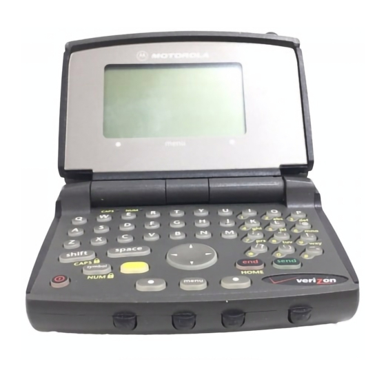
- Page 1 Level 3 Service Manual Dual Band Personal Communicator Motorola V200 CDMA 800/1900 MHz Technology...
-
Page 3: Table Of Contents
Level 3 Service Manual Table of Contents 6881039B10 Table of Contents Introduction ............. . . 1 Product Identification . - Page 4 Table of Content s CDMA V200 October 04, 2001 6881039B10...
-
Page 5: Introduction
Available on a contract basis, Motorola Inc. offers comprehensive maintenance and installation programs which enable customers to meet requirements for reliable, continuous communications. To learn more about the wide range of Motorola service programs, contact your local Motorola products representative or the nearest Customer Service Manager. Product Identification Motorola products are identified by the model number on the housing. -
Page 6: Computer Program Copyrights
The Motorola products described in this manual may include Motorola computer programs stored in semiconductor memories or other media that are copyrighted with all rights reserved worldwide to Motorola. Laws in the United States and other countries preserve for Motorola, Inc. certain exclusive rights to the copyrighted... -
Page 7: Warranty Service Policy
Product Support Customer’s original units will be repaired but not refurbished as standard. Appoint- ed Motorola Service Hubs will perform warranty and non-warranty field service for level 2 (assemblies) and level 3 (limited PCB component). The Motorola Hi-Tech Centers will perform level 4 (full component) repairs. -
Page 8: Parts Replacement
When ordering crystals or channel elements, specify the Motorola part number, description, crystal frequency, and operating frequency desired. When the Motorola part number of a component is not known, use the product model number or other related major assembly along with a description of the related major assembly and of the component in question. -
Page 9: Circuit Description
Communication with accessories is through the CE bus connector through the audio/power controller IC. Audio through the external connector is analog. The V200 has an integrated speakerphone that also serves as the alert transduc- er. The audio/power controller IC handles all the audio functions including alert/ speakerphone and headset speaker/microphone. - Page 10 EXCITER RF/DISPLAY BOARD POWER AMPLIFIER TRANSCEIVER LI-ION BATTERY MICROCOMPUTER FLASH CALL PROCESSOR FLIP ASSY VIBRATOR QWERTY KEYBOARD HEADSET JACK AUDIO/POWER CONTROLLER CE BUS CONNECTOR SPEAKER- PHONE CONTROLLER BOARD /ALERT 010992o Figure 1. V200 simplified block diagram October 04, 2001 6881039B10...
-
Page 11: Controller
Level 3 Service Manual Circuit Description Transceiver (RF Circuit) The V200 transceiver chip set includes Motorola front-end (FE), mixer/exciter (ME), and RF transceiver ICs. Refer to Figure 1. Switching between the antenna and accessory antenna port is mechanical, having a normally-closed circuit with the antenna connector. When an accessory RF plug is inserted, the switch opens the antenna circuit and closes the accessory port circuit. - Page 12 CE Bus Connector J1000 AUDIO_GND BATT_GND 010993o Figure 2. V200 controller block diagram Transmit Audio from the internal speakerphone microphone or headset microphone is routed through, and amplified by, audio/power controller IC U1200. From U1200, the transmit audio is sent to call processor IC U1100 on the MIC1 and MICREF lines.
- Page 13 Figure 3 is a simplified diagram of the keypad logic. 010994o Figure 3. V200 keypad logic The keys on the PCB use a three contact design. One of the contacts is tied to ground while the other two are pulled high (2.7 V) and connected to the rows and columns inputs.
- Page 14 Circuit Description CDMA V200 The Figure 4 shows The V200 keypad mapping. 010995o Figure 4. V200 keypad mapping October 04, 2001 6881039B10...
- Page 15 Level 3 Service Manual Circuit Description Memory Interface The call processor IC U1100 has access, via its parallel data bus, to 1 SRAM (256k X 16) U1400 in a 48-ball uBGA and 1 32 Mbit (2 Mbit x 16) Read-While-Write capable burst flash EPROM U1300 in a 56-ball uBGA/FBGA (this part combines EEPROM and Flash ROM functionality).
- Page 16 TEMP_SENSE Input to the measurement ADC from thermistor. CE Bus Connector V200 Personal Communicators have the Motorola CE Bus interface. The bus incorporates RS232 serial communication and universal serial bus (USB) into one connector. The CE Bus supports connection to accessories, personal computers, and test systems.
-
Page 17: Transceiver
RS232 requires a Motorola RS232 data head to interface to a PC. In the V200 CE Bus pin 2 serves the dual functions of BATTFDBK and MANTST. BATTFDBK is used for controlled power dissipation by the charger. MANTST is used to detect the type of charger (Full rate, Mid rate, and Invalid). - Page 18 Q1307 010996o Figure 5. V200 transceiver block diagram Transmit CDMA Cellular 800 MHz (PCS 1900 MHz) TXIP, TXIM, TXQP, and TXQM from call processor IC U1100 modulate the transmit offset VCO (Q652) signal which is external to, but controlled by, RF transceiver IC U700.
- Page 19 Level 3 Service Manual Circuit Description Frequency Synthesizer Circuitry V200 transceivers contain 4 oscillators controlled by 3 PLLs located within RF transceiver IC U700. All the PLLs obtain their reference frequency from the 16.8 MHz reference oscillator. • Main LO consists of 2 VCO modules external to U700.
- Page 20 Circuit Description CDMA V200 October 04, 2001 6881039B10...
-
Page 21: Tools And Test Equipment
Power supply cable Used with CDMACOMM. 1. To order in North America, contact Motorola Aftermarket and Accessories Division (AAD) by phone at (800) 422-4210 or FAX (800) 622-6210; Internationally, AAD can be reached by calling (847) 538-8023 or faxing (847) 576-3023. - Page 22 Powers UUT. Used with PST. 1. To order in North America, contact Motorola Aftermarket and Accessories Division (AAD) by phone at (800) 422-4210 or FAX (800) 622-6210; Internationally, AAD can be reached by calling (847) 538-8023 or faxing (847) 576-3023.
-
Page 23: Programming
Phasing is performed at Level 3 and above service centers and by carriers. It includes alignment of the communicator’s RF circuitry. The computer test mode via Motorola CDMACOMM software is used by Level 3 centers for phasing V200 communicators. Flexing Flexing involves configuring the communicator’s features and functionality. - Page 24 Programming CDMA V200 October 04, 2001 6881039B10...
-
Page 25: Test Methods
RF functionality and for NAM programing. All tests are performed directly from the communicator’s keyboard without need for additional test equipment. For detailed information about manual test mode, refer to the V200 Level 2 Service Manual listed in the Related Publications section toward the end of this manual. -
Page 26: Troubleshooting
Defective circuit boards should be forwarded to the appropriate Motorola service facility for repair. Refer to the V200 Level 3 Supplements listed in the Related Publications section of this manual for a list of replacement part descriptions and part numbers. - Page 27 Level 3 Service Manual Troubleshooting • After the successful entry of Data Mode and Suspend, select and/or set the fields highlighted in yellow (white) as shown in the screen image correspond- ing to the procedure being performed. PC RUNNING CDMACOMM SOFTWARE COMMUNICATIONS ANALYZER 2888482K03 AUDIO CABLES...
- Page 28 Troubleshooting CDMA V200 Loopback (Boom Mic Speaker) • Select the SUSPEND button to put the phone into Suspend Mode. • Select CDMA 800 button under CP_MODE to put the UUT in 800 CDMA Mode. • Under AUD_PATH command, set Input to 4 and Output to 6 to route Audio to/ from Headset Jack.
- Page 29 Level 3 Service Manual Troubleshooting 010998o Figure 7. Loopback 6881039B10 October 04, 2001...
- Page 30 Troubleshooting CDMA V200 DTMF Deviation This phasing procedure is used to phase the deviation that results from normal audio levels. Table 4. DTMF Deviation Test Values Parameter Value Test Voltage at Battery Terminals 3.60V Test Voltage at Acc. Connector 4.40V...
- Page 31 Level 3 Service Manual Troubleshooting 010999o Figure 8. DTMF deviation 6881039B10 October 04, 2001...
- Page 32 Troubleshooting CDMA V200 Maximum Deviation This phasing procedure is used to insure that the communicator will produce an FM deviation no greater than a specified amount, even in the event that the communicator modulator is presented with a large audio signal.
- Page 33 Level 3 Service Manual Troubleshooting 011000o Figure 9. Maximum deviation 6881039B10 October 04, 2001...
- Page 34 Troubleshooting CDMA V200 Microphone Audio Deviation This phasing procedure is used to phase the deviation that results from normal audio levels. Table 6. Microphone Audio Deviation Test Values Parameter Value Test Voltage at Battery Terminals 3.60V Test Voltage at Acc. Connector 4.40V...
- Page 35 Level 3 Service Manual Troubleshooting 011001o Figure 10. Microphone audio deviation 6881039B10 October 04, 2001...
- Page 36 Troubleshooting CDMA V200 RX Audio Gain This phasing procedure is used to phase the deviation that results from normal audio levels. Table 7. RX Audio Gain Test Values Parameter Value Test Voltage at Battery Terminals 3.60V Test Voltage at Acc. Connector 4.40V...
- Page 37 Level 3 Service Manual Troubleshooting 011002o Figure 11. RX audio gain 6881039B10 October 04, 2001...
- Page 38 Troubleshooting CDMA V200 RX Audio Muting Table 8. RX Audio Muting Test Values Test Limits Level (dB) Upper limit -40.0 Lower limit -90.0 • Select the SUSPEND button to put the phone into Suspend Mode. • Under CP_MODE, select the AMPS button to place the transceiver into Analog call processing mode.
- Page 39 Level 3 Service Manual Troubleshooting 011003o Figure 12. RX audio muting 6881039B10 October 04, 2001...
- Page 40 Troubleshooting CDMA V200 RX Distortion Table 9. RX Distortion Test Values Distortion Level Distortion Level Test Limits (dB) Upper limit -26.0 Lower limit -60.0 • Select the SUSPEND button to put the phone into Suspend Mode. • Under CP_MODE, select the AMPS button to place the transceiver into Analog call processing mode.
- Page 41 Level 3 Service Manual Troubleshooting 011004o Figure 13. RX distortion 6881039B10 October 04, 2001...
- Page 42 Troubleshooting CDMA V200 RX Hum and Noise Table 10. RX Hum and Noise Test Values RX Hum & Noise Level (dB) Upper limit Lower limit • Select the SUSPEND button to put the phone into Suspend Mode. • Under CP_MODE, select the AMPS button to place the transceiver into Analog call processing mode.
- Page 43 Level 3 Service Manual Troubleshooting 011005o Figure 14. RX hum and noise 6881039B10 October 04, 2001...
- Page 44 Troubleshooting CDMA V200 RX Response Table 11. RX Response Test Values Test Limits Level at 300 Hz Level at 300 kHz Upper limit 11.5 -8.5 Lower limit -15.6 • Select the SUSPEND button to put the phone into Suspend Mode.
- Page 45 Level 3 Service Manual Troubleshooting 011006o Figure 15. RX response 6881039B10 October 04, 2001...
- Page 46 Troubleshooting CDMA V200 SAT Deviation This phasing procedure is used to phase the deviation that results from normal audio levels. Table 12. SAT Deviation Test Values Parameter Value Test Voltage at Battery Terminals 3.60V Test Voltage at Acc. Connector 4.40V...
- Page 47 Level 3 Service Manual Troubleshooting 011007o Figure 16. SAT deviation 6881039B10 October 04, 2001...
- Page 48 Troubleshooting CDMA V200 Signaling Tone Deviation This phasing procedure is used to phase the deviation that results from normal audio levels. Table 13. Signaling Tone Deviation Test Values Parameter Value Test Voltage at Battery Terminals 3.60V Test Voltage at Acc. Connector 4.40V...
- Page 49 Level 3 Service Manual Troubleshooting 011008o Figure 17. Signaling tone deviation 6881039B10 October 04, 2001...
- Page 50 Troubleshooting CDMA V200 RX Sensitivity (SINAD) Table 14. RX Sensitivity (SINAD) Test Values Parameter Value Lower limit Upper limit Channel (1) Channel (2) Channel (3) • Select the SUSPEND button to put the phone into Suspend Mode. • Under CP_MODE, select the AMPS button to place the transceiver into Analog call processing mode.
- Page 51 Level 3 Service Manual Troubleshooting 011009o Figure 18. RX sensitivity (SINAD) 6881039B10 October 04, 2001...
- Page 52 Troubleshooting CDMA V200 TX Audio Muting Table 15. TX Audio Muting Test Values Test Limits Level (dB) Upper limit -40.0 Lower limit -90.0 • Select the SUSPEND button to put the phone into Suspend Mode. • Under CP_MODE, select the AMPS button to place the transceiver into Analog call processing mode.
- Page 53 Level 3 Service Manual Troubleshooting 011010o Figure 19. TX audio muting 6881039B10 October 04, 2001...
- Page 54 Troubleshooting CDMA V200 TX Distortion Table 16. TX Distortion Test Values Distortion Level Distortion Level Test Limits (dB) Upper limit -26.0 Lower limit -60.0 • Select the SUSPEND button to put the phone into Suspend Mode. • Under CP_MODE, select the AMPS button to place the transceiver into Analog call processing mode.
- Page 55 Level 3 Service Manual Troubleshooting 011011o Figure 20. TX distortion 6881039B10 October 04, 2001...
- Page 56 Troubleshooting CDMA V200 TX Hum and Noise Table 17. TX Hum and Noise Test Values TX Hum and Noise Level (dB) Upper limit Lower limit • Select the SUSPEND button to put the phone into Suspend Mode. • Under CP_MODE, select the AMPS button to place the transceiver into Analog call processing mode.
- Page 57 Level 3 Service Manual Troubleshooting 011012o Figure 21. TX hum and noise 6881039B10 October 04, 2001...
- Page 58 Troubleshooting CDMA V200 TX Response Table 18. TX Response Test Values Level at 300 Hz Level at 3 kHz Test Limits (dB) (dB) Upper limit 10.5 Lower limit -13.5 • Select the SUSPEND button to put the phone into Suspend Mode.
- Page 59 Level 3 Service Manual Troubleshooting 011013o Figure 22. TX response 6881039B10 October 04, 2001...
- Page 60 Troubleshooting CDMA V200 Receiver Sensitivity (FER) Table 19. Receiver Sensitivity (FER) Test Values Parameter CDMA LOW_CHANNEL 1013 MID_CHANNEL HIGH_CHANNEL 1175 13K_DATA_TRAF_LEVEL -12.3 dB -12.3 dB -104 dBm -104 dBm RX_LEVEL (-102 dBm @ (-102 dBm @ HOT thermal) HOT thermal) FER_LIMIT 0.5% FER...
- Page 61 Level 3 Service Manual Troubleshooting 800 FER Screen 1 800 FER Screen 2 PCS FER Screen 1 PCS FER Screen 2 011014o Figure 23. Receiver sensitivity (FER) 6881039B10 October 04, 2001...
- Page 62 Troubleshooting CDMA V200 Receiver Sensitivity in the Presence of Noise (FER in AWGN) The test channels are given below. Table 20. Receiver Sensitivity in the Presence of Noise Test Values Parameter CDMA Test voltage at battery terminals 3.60V 3.60V Test voltage at accessory connector 4.40V...
- Page 63 Level 3 Service Manual Troubleshooting 800 FERAWGN Screen 1 800 FER AWGN Screen 2 PCS FER AWGN Screen 1 PCS FER AWGN Screen 2 011015o Figure 24. Receiver sensitivity in the presence of noise 6881039B10 October 04, 2001...
- Page 64 Troubleshooting CDMA V200 Quality (Rho) Table 21. Quality (Rho) Test Values Parameter CDMA RF_LEVEL -73 dBm -76 dBm Upper limit 1.000 1.000 Lower limit 0.944 0.944 • Phone should be powered on and in a 13K/RateSet2 CDMA Full Rate Data Call.
- Page 65 Level 3 Service Manual Troubleshooting 800 RHO Screen 1 800 RHO Screen 2 PCS RHO Screen 1 PCS RHO Screen 2 011016o Figure 25. Quality (Rho) 6881039B10 October 04, 2001...
- Page 66 Troubleshooting CDMA V200 Splatter at Maximum Output Power Table 22. Splatter Test Values Parameter CDMA Test voltage at battery terminals 3.60V 3.60V Test voltage at accessory connector 4.40V 4.40V RX_LEVEL -104 dBm -104 dBm SPLATTER_LIMIT -42 dBc / 30 kHz -42 dBc / 30 kHz FREQUENCY_OFFSET_HIGH +0.885 MHz...
- Page 67 Level 3 Service Manual Troubleshooting 800 Splatter Screen 1 800 Splatter Screen2 011017o Figure 26. Splatter 6881039B10 October 04, 2001...
-
Page 68: Troubleshooting Procedures
Troubleshooting CDMA V200 Troubleshooting Procedures The goal in troubleshooting is to quickly narrow down the possibilities to isolate a failure to a single faulty component. This is especially important before deciding to replace a multi-pin IC, filter, or other component that is difficult or risky to replace. - Page 69 Level 3 Service Manual Troubleshooting does not work. 10. SRAM troubleshooting. • IF SRAM_CS is toggling, go to step 11. • If problem still exists, reflow SRAM U1400, or replace U1400 if reflow does not work. 11. Audio/power controller IC U1200 troubleshooting. •...
- Page 70 Troubleshooting CDMA V200 • TEMPBIAS pin U1200 pin B1 not connected properly. • R9976 or R1244 not connected properly. Invalid battery message • BATT_SERIAL_DATA J870 pin 3 not connected properly. • GPIO8_OWIRE U1100 pin C9 not connected properly. • R1155 or R9917 not connected properly.
- Page 71 Level 3 Service Manual Troubleshooting Troubleshooting the Headset Speaker Prior to troubleshooting, make sure headset is working. Check headset jack J600, call processor IC INT1 U1100 pin E8, and R20212. No Receive Audio. • Test commands: Suspend, Headset speaker, Volume level, Speakerphone tone. 30000009000000360001000000 3000000A00000006000200004600 30000009000000050001000003...
- Page 72 Troubleshooting CDMA V200 30000009000000360001000000 3000000A00000006000200003400 30000009000000050001000003 3000000B000000000003000000002A • Send the above test commands to generate a tone to CE bus connector AUDIO_OUT J1000 pin 15. If the signal is present on J1000 pin 15 but no audio, J1000 may be defective.
- Page 73 Level 3 Service Manual Troubleshooting • If signal is coming out of AUDIOOUTP and AUDIOOUTM, check U1200 and the parts associated with A0A, A1 and A2 U1200 amplifiers. • If no signal is present at C1221 and C1212, either defective U1100 or cold solder / missing power supply to U1100.
-
Page 74: Test Points
• If voice can’t be heard while talking in to the microphone, U1100 or the modu- lator/demodulator may be defective. Test Points Controller Board Refer to Table 23, Table 24, and the appropriate V200 Level 3 Supplement for test point locations and functions. Table 23. V200 Controller Board Test Points Test Point... -
Page 75: Connector Signals And Pin Assignments
JBB1 and P1 (controller and transceiver board, respectively). Table 25 shows the signal associated with each connector pin. For connector and pin locations, refer to the V200 Level 3 Supplement listed in the Related Publications section toward 6881039B10 October 04, 2001... - Page 76 Troubleshooting CDMA V200 the end of this manual. Refer to Table 1 for a description of the signal names shown in Table 25. Table 25. Board-to-Board Interface Pin Assignments Controller JBB1 Transceiver P1 Controller JBB1 Transceiver P1 RX_ 2.75V RX_ 2.75V_UN PAH_ B+ RX_ 2.75V...
- Page 77 Level 3 Service Manual Troubleshooting Table 25. Board-to-Board Interface Pin Assignments (Continued) Controller JBB1 Transceiver P1 Controller JBB1 Transceiver P1 Ground RF_GND Ground RF_GND OSCEN_b Ground RF_GND TEMP_ SENSE Controller Board Connectors JDIS1, J1000, J600, J870, and J7000 Tables 26 through 30 show signals associated with the connectors located on the controller board.
- Page 78 Troubleshooting CDMA V200 Table 27. CE Bus Connector J1000 Pin Assignments Pin(s) Signal Name Function 1 BATT_ GND Power ground 2 BATT_FDBK Default, battery feedback USB / RS232 (6 wire) 3 RAWEXTB+ External power USB+ Default TXD (D+) USB, RS232 (8 wire), USB / RS232 (6 wire), Smart Audio...
- Page 79 Level 3 Service Manual Troubleshooting Table 28. Headset Jack J600 Pin Assignments Pin(s) Signal Name Function 1 GND Ground 2 SWI 3 SP Speaker 4 MIC Microphone 5 BRK Table 29. Battery Connector J870 Pin Assignments Pin(s) Signal Name Function Ground 2 BATT_TEMP 3 BATT_SERIAL_DATA...
- Page 80 Troubleshooting CDMA V200 October 04, 2001 6881039B10...
-
Page 81: Part Numbers
Part Numbers Part Numbers The following charts show the transceivers and related publications associated with V200 communicator models currently available. Related Publications V200 Level 1 and 2 Service Manual 6881039B05 V200 Level 3 Controller Supplement 6881104B88 V200 Level 3 Transceiver Supplement... -
Page 82: Model Chart
Part Numbers CDMA V200 Model Chart Use Table 33 to identify the specific board assemblies used in each model V200 communicator. Table 33. V200 Personal Communicator Model Chart MODEL 82701GHESA V200 CDMA Sales Model 82702GHESA V200 CDMA Sales Model (replace with S9619 Field Replacement Unit) -
Page 83: Index
6881039B10 Index Level 3 Service Manual Index Index splatter test 62 transmit audio muting test 48 transmit distortion test 50 transmit hum and noise test 52 transmit response test 54 account product code (APC) 2 connector pin assignments 71 audience connectors service manual 2 board-to-board 71... - Page 84 Index CDMA V200 maximum deviation test 28 about 2 mechanical serial number (MSN) 2 audience 2 microphone audio deviation test 30 conventions 3 revisions 3 scope 2 service policy 3 names customer support 4 product 1 out of box failure 3...
- Page 86 MOTOROLA, the Stylized M Logo, and all other trademarks indicated as such herein are trademarks of Motorola, Inc. ® Reg. U.S. Pat. & Tm. Off. TrueSync and Starfish are registered trademarks of Starfish, Inc., a wholly owned independent subsidiary of Motorola, Inc.
Need help?
Do you have a question about the V200 and is the answer not in the manual?
Questions and answers