Table of Contents
Advertisement
Quick Links
SERVICE
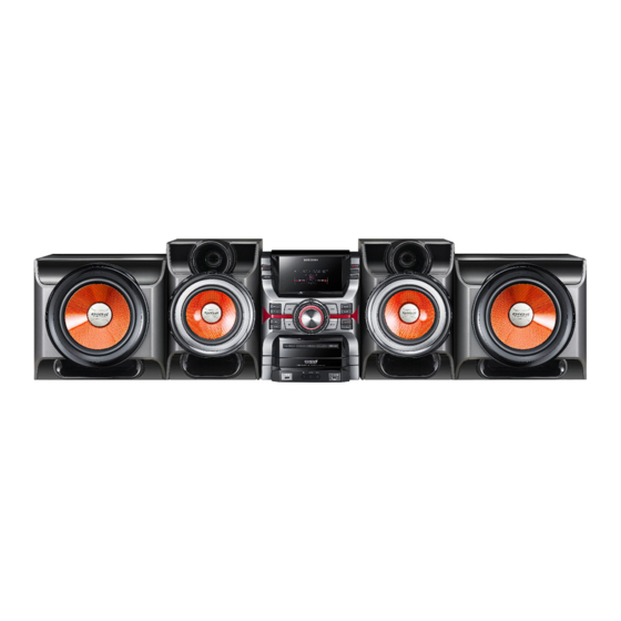
MINI-Compact System
MX-D850
Refer to the service manual in the GSPN (see the rear cover) for more information.
MINI-Compact System
Model Name
Model Code
MANUAL
1. Precaution
2. Product Specification
3. Disassembly & Reassembly
4. Troubleshooting
5. PCB Diagram
6. Schematic Diagram
MX-D850
MX-D850/ZP
Contents
Advertisement
Table of Contents

Related Manuals for Samsung MX-D850


Summary of Contents for Samsung MX-D850
- Page 1 MINI-Compact System Model Name MX-D850 Model Code MX-D850/ZP SERVICE MANUAL MINI-Compact System Contents 1. Precaution 2. Product Specification 3. Disassembly & Reassembly MX-D850 4. Troubleshooting 5. PCB Diagram 6. Schematic Diagram Refer to the service manual in the GSPN (see the rear cover) for more information.
-
Page 2: Table Of Contents
Product Feature ........................2 − 1 2.1.1. MX-D830 Product Feature .................... 2 − 1 2.1.2. MX-D830D Product Feature..................2 − 2 2.1.3. MX-D850 Product Feature .................... 2 − 3 2.1.4. MX-D870 Product Feature .................... 2 − 4 2.1.5. MX-D870D Product Feature..................2 − 5 2.2. - Page 3 Test Point Wave Form ....................6 − 6 6.6. MAIN–2 ..........................6 − 7 6.7. MAIN–3 ..........................6 − 8 6.8. MAIN–4 ..........................6 − 9 6.9. MAIN–5 ..........................6 − 10 6.10. MAIN–6 ..........................6 − 11 Copyright© 1995-2011 SAMSUNG. All rights reserved.
-
Page 4: Precaution
TES T ALL EXPO S ED METAL SU RFACES 2-WIRE CORD ALSO TES T WITH PLUG REVER S ED (US ING AC EARTH ADAPTER P LUG GROUND AS R EQ UIRED) Figure 1.1 AC Leakage Test Copyright© 1995-2011 SAMSUNG. All rights reserved. - Page 5 A replacement part that does not have the same safety characteristics as the original might create shock, fire or other hazards. Copyright© 1995-2011 SAMSUNG. All rights reserved.
-
Page 6: Servicing Precautions
CAUTION First read the “Safety Precautions” section of this manual. If some unforeseen circumstance creates a conflict between the servicing and safety precautions, always follow the safety precautions. Copyright© 1995-2011 SAMSUNG. All rights reserved. -
Page 7: Precautions For Electrostatically Sensitive Devices (Esds)
8) Minimize body motions when handling unpackaged replacement ESDs. Motions such as brushing clothes together, or lifting a foot from a carpeted floor can generate enough static electricity to damage an ESD. Copyright© 1995-2011 SAMSUNG. All rights reserved. -
Page 8: Product Specification
Twin USB • GiGA Sound ■ Connectivity • USB Host • Portable Audio In (3.5 phi Stereo Jack) ■ Disc • Type : 3 Tray • Compatible : MP3, CD / CD-R, RW, WMA Copyright© 1995-2011 SAMSUNG. All rights reserved. -
Page 9: Mx-D830D Product Feature
Portable Audio In (3.5 phi Stereo Jack) ■ Disc • Type : 3 Tray • Compatible : DVD, Divx, MP3, CD / CD-R, RW, WMA, VCD (Regional Option) • Video Out : Component / Composite Copyright© 1995-2011 SAMSUNG. All rights reserved. -
Page 10: Mx-D850 Product Feature
Twin USB • GiGA Sound ■ Connectivity • USB Host • Portable Audio In (3.5 phi Stereo Jack) ■ Disc • Type : 3 Tray • Compatible : MP3, CD / CD-R, RW, WMA Copyright© 1995-2011 SAMSUNG. All rights reserved. -
Page 11: Mx-D870 Product Feature
• Twin USB • GiGA Sound ■ Connectivity • USB Host • Portable Audio In (3.5 phi Stereo Jack) ■ Disc • Type : 3 Tray • Compatible : MP3, CD / CD-R, RW Copyright© 1995-2011 SAMSUNG. All rights reserved. -
Page 12: Mx-D870D Product Feature
Portable Audio In (3.5 phi Stereo Jack) ■ Disc • Type : 3 Tray • Compatible : DVD, Divx, MP3, CD / CD-R, RW, WMA, VCD (Regional Option) • Video Out : Component / Composite Copyright© 1995-2011 SAMSUNG. All rights reserved. -
Page 13: Specifications
MX-D830- 560 Watts (10% THD) 280W/CH (6 Ω/100Hz) Front speaker MX-D830- 640 Watts (MAX. THD) Front speaker 320W/CH (6 Ω/100Hz) MX-D850- 760 Watts (10% THD) Front speaker 280W/CH (6 Ω/100Hz) 200W/CH (8 Ω/100Hz) Subwoofer MX-D850- 860 Watts (MAX. THD) Output Front speaker 310W/CH (6 Ω/100Hz) -
Page 14: Specifications Analysis
38 KEY 32 KEY 32 KEY DUAL VOLTAGE Front : 3 Ohm SPK IMPEDANCE 4 Ohm 4 Ohm 4 Ohm S/W : 4 Ohm Rear : 6 Ohm O: Feature Included, X: Not Included Copyright© 1995-2011 SAMSUNG. All rights reserved. - Page 15 REMOTE KEY 38 KEY 38 KEY 32 KEY DUAL VOLTAGE Front : 3 Ohm SPK IMPEDANCE 4 Ohm 4 Ohm S/W : 4 Ohm Rear : 6 Ohm O: Feature Included, X: Not Included Copyright© 1995-2011 SAMSUNG. All rights reserved.
-
Page 16: Accessories
2. Product Specification 2.4. Accessories 2.4.1. Supplied Accessories Accessories Item Item code Remark Remote Control AH59-02363A Batteries 4301-000121 FM Antenna AH42-00021A Local Samsung Dealer AM Antenna AH42-00035A AH68-02331B User’s Manual AH68-02331C Copyright© 1995-2011 SAMSUNG. All rights reserved. -
Page 17: Disassembly & Reassembly
In order to assemble reverse the order of disassembly. CAUTION Be careful not to make any scratches as you remove them. 1. Power on and open the disk, Separate CD-Door. 3. Unfasten 2 screws. : BH,+,B,M3,L10,ZPC(BLK),SWRCH18A Copyright© 1995-2011 SAMSUNG. All rights reserved. - Page 18 3. Disassembly & Reassembly 4. Unfasten 2 screws. 6. Pull up and remove CABINET-TOP. : BH,+,B,M3,L10,ZPC(BLK),SWRCH18A 5. Remove CABINET-LEFT and CABINET-RIGHT. 7. Remove FRONT ASSY. Copyright© 1995-2011 SAMSUNG. All rights reserved.
- Page 19 3. Disassembly & Reassembly 8. Unplug this 3 wire and 3 cables. 10. Unfasten 3 screws. : BH,+,-,B,M3,L10,ZPC(WHT),SWRCH18A 11. Unfasten 14 screws. : BH,+,-,B,M3,L10,ZPC(WHT),SWRCH18A 9. Unplug the Volume Knob. Copyright© 1995-2011 SAMSUNG. All rights reserved.
- Page 20 12. Unplug this two holder. 15. Unplug the Fan wire. 16. Unplug this 3 cable and 2 wire. 13. Unfasten 2 screws. : BH,+,-,B,M3,L10,ZPC(WHT),SWRCH18A 17. Unfasten 11 screws. : BH,+,-,B,M3,L10,ZPC(WHT),SWRCH18A 14. Unfasten 7 screws. : BH,+,B,M3,L10,ZPC(BLK),SWRCH18A Copyright© 1995-2011 SAMSUNG. All rights reserved.
- Page 21 18. Unplug this 2 cable. 21. Unplug gear boxes of each side (left, right). 22. Unfasten the 4 screws. : BH,+,B,M3,L10,ZPC(BLK),SWRCH18A 19. Remove this spring. 20. Unfasten the 4 screws. : BH,+,B,M3,L10,ZPC(BLK),SWRCH18A 23. Disassemble Top Assy . Copyright© 1995-2011 SAMSUNG. All rights reserved.
- Page 22 3. Disassembly & Reassembly 24. Remove TOP-LED PCB Assy . 25. TOP-LED PCB Assy (LED). Copyright© 1995-2011 SAMSUNG. All rights reserved.
-
Page 23: Troubleshooting
4. Troubleshooting 4. Troubleshooting 4.1. Checkpoints by Error Mode Oscilloscope Setting Values Normal Voltage 24MHz 32.768KHz Voltage/DIV 1Vol/DIV 1Vol/DIV 1Vol/DIV TIME/DIV 1uS/DIV 10ns/DIV 0.1uS/DIV Copyright© 1995-2011 SAMSUNG. All rights reserved. -
Page 24: No Power
Che ck s igna l a nd s igna l circu it in MAIN P CB UX1, UX2 pa tte rn. pa rt ok? Ye s Che ck pa tte rn or re pla ce MICOM IC. Copyright© 1995-2011 SAMSUNG. All rights reserved. - Page 25 4. Troubleshooting 100OHM 100OHM 100NF 100NF UIC1 UIC1 LC87F5NC8 AVU LC87F5NC8 AVU 10 0 10 0 UAR5 UAR5 100OHM 100OHM DGND DGND * 6.5. MAIN-1 UIC1 * 5.6. MAIN P CB Top <Fig. 4-1> Copyright© 1995-2011 SAMSUNG. All rights reserved.
-
Page 26: No Output
Che ck MICOM IC s igna l pa tte rn or re place (UIC1) a nd IC1 MPE G S MP S . (ESS) signal? Ye s Re pla ce UIC1 and IC 1. Copyright© 1995-2011 SAMSUNG. All rights reserved. -
Page 27: Measures To Be Taken When The Protection Circuit Operates
Protection Circuit operates when power problem occurs in the SMPS. Protection Circuit Operation Location Pin No. Remark Open Short +8V (5, 8) SMPS PCB CON803 D5.6V (1, 2, 3) PVDD (about +55V) (14 ~ 19) ○ CON802 -55V (1 ~ 6) ○ Copyright© 1995-2011 SAMSUNG. All rights reserved. -
Page 28: Check Amp In Power Protection
14Ω If Measured Resistance is very different from above numbers, There is a Problem. → AMP PART Problem 4.2CH SP EAKER OUTPUT REAR R REAR L SUBWOOFER R SUBWOOFER L FRONT R FRONT L Copyright© 1995-2011 SAMSUNG. All rights reserved. -
Page 29: Micom, Mpeg Initialization & Update
3) The disc is automatically ejected. (If you use USB memory, detach USB memory.) ■ MPEG Reset • During “No Disc” displayed, push the stop button 5 seconds. After displayed “INITIALIZE” set will power off automatically. Copyright© 1995-2011 SAMSUNG. All rights reserved. -
Page 30: Buyer-Region Code Setting Method
• The region code is inserted by the remote control. 1) Press “FUNCTION” button several times to change to AUX mode. <MX-D830 / MX-D850 / MX-D870> <MX-D830D / MX-D870D> 2) Press “ENTER” button more than 5 seconds. <MX-D830 / MX-D850 / MX-D870>... - Page 31 3) After step (2), you can see “TEST − −” on the VFD. Insert number “46” to select Region Code. 4) After step (3), you can see “− − −” on the VFD. Insert the Region Code corresponding model with “0 ~ 9” buttons on the remote control. 5) Turn the Power off. Copyright© 1995-2011 SAMSUNG. All rights reserved.
- Page 32 4. Troubleshooting Table 4.1 MX-D870 / MX-D830 / MX-D850 Option Table Buyer MX-D870 Region Code MX-D830 / MX-D850 Region Code Africa, Pakistan Brazil China (semi_mic) Europe Indonesia, Hong Kong Japan Korea Latin American Mexico Philippines Russia (full_mic) Russia (semi_mic) South Africa...
- Page 33 Indonesia, Hong Kong Japan Korea Latin American Mexico Philippines Russia (full_mic) Russia (semi_mic) South Africa Taiwan USA, Canada New Zealand, Australia England Iran (HACO) India Israel Middle Asia, Morocco, Algeria Asia Singapore Panama Copyright© 1995-2011 SAMSUNG. All rights reserved. 4-11...
-
Page 34: Pcb Diagram
LED LIGHTING LED LIGHTING 3 CD C HANGER 3 CD C HANGER US B US B US B J ACK US B J ACK AUX IN AUX IN MIC IN MIC IN SMPS SMPS Copyright© 1995-2011 SAMSUNG. All rights reserved. -
Page 35: Key Pcb Top
5. PCB Diagram 5.2. KEY PCB Top Copyright© 1995-2011 SAMSUNG. All rights reserved. -
Page 36: Key Pcb Bottom
5. PCB Diagram 5.3. KEY PCB Bottom Copyright© 1995-2011 SAMSUNG. All rights reserved. -
Page 37: Vfd Pcb Top
5. PCB Diagram 5.4. VFD PCB Top VFCN2 JCN1 USCN2 USCN1 VC N 1 Copyright© 1995-2011 SAMSUNG. All rights reserved. -
Page 38: Pin Connection
REC_LED VFD_GND KEY_AD2 4) USCN1 KEY_AD1 USB1 REMO Pin No. Signal VFD_GND USB1_5V VFD_GND USB1_DN 5.8V USB1_DP 5.8V USB1_GND UART_RX UART_TX 5) USCN2 5.6V USB2 Pin No. Signal USB1_LED USB2_5V USB2_DN USB1_DP USB2_GND USB2_LED Copyright© 1995-2011 SAMSUNG. All rights reserved. -
Page 39: Vfd Pcb Bottom
5. PCB Diagram 5.5. VFD PCB Bottom VFCN2 JCN1 USCN2 USCN1 VC N 1 Copyright© 1995-2011 SAMSUNG. All rights reserved. -
Page 40: Main Pcb Top
5. PCB Diagram 5.6. MAIN PCB Top (12) FL CN1 FR CN1 (11) RFIC1 IPIC1 UIC4 MIC2 MCN2 USIC1 UT CN1 UIC1 AIC1 AIC2 TO P CN1 (10) CON13 AJK1 Copyright© 1995-2011 SAMSUNG. All rights reserved. -
Page 41: Pin Connection
5) UTCN1 MICOM Update Port 2) RMCN1 8) TOPCN1 Sled Control Party Lighting Pin No. Signal U_5V Pin No. Signal Pin No. Signal DBGP2 SLED+ Blue DBGP1 SLED- Green DBGP0 DCMO- DGND DCMO+ 5.6V Copyright© 1995-2011 SAMSUNG. All rights reserved. - Page 42 FRLED3 -55V FRLED4 -55V FRLED5 -55V FRLED6 SGND SGND SGND SGND SGND SGND SGND +55V +55V +55V +55V +55V +55V 11) FLCN1 Speaker LED Connector Pin No. Signal FRLED1 FRLED2 FRLED3 FRLED4 FRLED5 FRLED6 Copyright© 1995-2011 SAMSUNG. All rights reserved.
-
Page 43: Test Point Wave Form
5. PCB Diagram 5.6.2. Test Point Wave Form Copyright© 1995-2011 SAMSUNG. All rights reserved. 5-10... -
Page 44: Main Pcb Bottom
5. PCB Diagram 5.7. MAIN PCB Bottom FAC N1 MCN2 UT CN1 CON13 AJK1 5-11 Copyright© 1995-2011 SAMSUNG. All rights reserved. -
Page 45: Schematic Diagram
OD over us b Con trol Crys tal Pr o 4 ch IR Amp Function Audio AUDIO & IR- FET Input Decode r Pre_AM P S W1 PW M/DAC S W2 Mic AMP dphone OP AMP Copyright© 1995-2011 SAMSUNG. All rights reserved. -
Page 46: Front-Key
TP 15 FR54 FR54 5.6V 5.6V 5.6V 5.6V 5.8V 5.8V DGND DGND REMO REMO KEY_AD2 KEY_AD2 DGND DGND KEY_AD3 KEY_AD3 J OG_UP J OG_UP J OG_DN J OG_DN DGND DGND DGND DGND DGND DGND Copyright© 1995-2011 SAMSUNG. All rights reserved. -
Page 47: Front-Volume
VS W7 VOL_LD6_V VOL_LD6_V VOL_LD8_V VOL_LD8_V VOL_LD7_V VOL_LD7_V VDGND VDGND VDGND VDGND VDGND VDGND VOL_LD3_V VOL_LD3_V VOL_LD4_V VOL_LD4_V VOL_LD5_V VOL_LD5_V VOL_LD1_V VOL_LD1_V VOL_LD2_V VOL_LD2_V VDGND VDGND VDGND VDGND VDGND VDGND VDGND VDGND VDGND VDGND Copyright© 1995-2011 SAMSUNG. All rights reserved. -
Page 48: Front-Jack/Vfd
VFDGND VFDGND 1/8W 1/8W VFDGND VFDGND 220OHM 220OHM KS C1008-Y KS C1008-Y 100UF 100UF GCC02-0077 GCC02-0077 MJACK1 MJACK1 MIC1 MIC1 100UF 100UF VFD PCB VFD PCB J ACK P CB J ACK P CB Copyright© 1995-2011 SAMSUNG. All rights reserved. -
Page 49: Main-1
JOG_UP JOG_UP JO G_DO WN JO G_DO WN JOG_DOW N JOG_DOW N VFD_GND VFD_GND VFD_GND VFD_GND VFD_VP VFD_VP VF_VP VF_VP -VFD -VFD -VFD -VFD MGND1 MGND1 +VFD +VFD +VFD +VFD VF_GND VF_GND DGND DGND Copyright© 1995-2011 SAMSUNG. All rights reserved. -
Page 50: Test Point Wave Form
6. Schematic Diagram 6.5.1. Test Point Wave Form Copyright© 1995-2011 SAMSUNG. All rights reserved. -
Page 51: Main-2
TUTP 6 TUTP 6 TU_R S T TU_R S T TUTP 5 TUTP 5 TU_C E TU_C E TUR16 TUR16 10KOHM 10KOHM TU_DA TU_DA TU_C LK TU_C LK TGND TGND TUAR1 TUAR1 100OHM 100OHM Copyright© 1995-2011 SAMSUNG. All rights reserved. -
Page 52: Main-3
OP 3 -55V -55V UR101 UR101 S _GND S _GND DGND DGND 2203-007598 2203-007598 AGND AGND ROP T1 ROP T1 0OHM 0OHM ROP T2 ROP T2 0OHM 0OHM AGND AGND S _GND S _GND Copyright© 1995-2011 SAMSUNG. All rights reserved. -
Page 53: Main-4
S BT42 -55V -55V -55V -55V -55V -55V S _GND S _GND AJK1 AJK1 -55 V -55 V S_GND S_GND AGND AGND -55V -55V 100V -> 50V CHANG E 100V -> 50V CHANG E Copyright© 1995-2011 SAMSUNG. All rights reserved. -
Page 54: Main-5
33OHM MR14 MR14 1KOHM 1KOHM M_ACK M_ACK MR16 MR16 1KOHM 1KOHM M_RXD M_RXD MP3.3V MP3.3V MR18 MR18 1KOHM 1KOHM M_PW M_RS T M_PW M_RS T 1KOHM 1KOHM MR20 MR20 M_RESE T M_RESE T 6-10 Copyright© 1995-2011 SAMSUNG. All rights reserved. -
Page 55: Main-6
USTP 9 SDB30A40- P F SDB30A40- P F DGND DGND USTP 10 USTP 10 4.7U F 4.7U F USB2_EN USB2_EN USB_LED2 USB_LED2 DGND DGND USB_LED1 USB_LED1 USB2_F AULT USB2_F AULT USTP 8 USTP 8 Copyright© 1995-2011 SAMSUNG. All rights reserved. 6-11... - Page 56 E.Asia, W.Asia, https://gspn2.samsungcsportal.com China, Japan N.America, S.America https://gspn3.samsungcsportal.com This Service Manual is a property of Samsung Electronics Co.,Ltd. © 2011 Samsung Electronics Co.,Ltd. Any unauthorized use of Manual can be punished under All rights reserved. applicable International and/or domestic law.
Need help?
Do you have a question about the MX-D850 and is the answer not in the manual?
Questions and answers