Table of Contents
Advertisement
Quick Links
SERVICE
MINI-Compact System
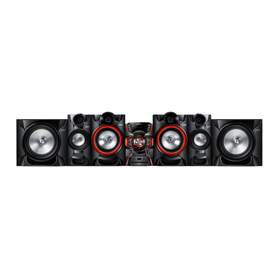
MX-F870
Refer to the service manual in the GSPN (see the rear cover) for more information.
MINI-Compact System
Model Name
Model Code
MANUAL
1. Precaution
2. Product Specification
3. Disassembly and Reassembly
4. Troubleshooting
5. PCB Diagram
6. Schematic Diagram
MX-F870
MX-F870/ZP
Contents
Advertisement
Table of Contents

Related Manuals for Samsung MX-F870


Summary of Contents for Samsung MX-F870
- Page 1 MINI-Compact System Model Name MX-F870 Model Code MX-F870/ZP SERVICE MANUAL MINI-Compact System Contents 1. Precaution 2. Product Specification 3. Disassembly and Reassembly MX-F870 4. Troubleshooting 5. PCB Diagram 6. Schematic Diagram Refer to the service manual in the GSPN (see the rear cover) for more information.
-
Page 2: Table Of Contents
Product Feature ........................2 − 1 2.1.1. Product Feature MX-F830/MX-F830B ................2 − 1 2.1.2. Product Feature MX-F850..................... 2 − 2 2.1.3. Product Feature MX-F870..................... 2 − 3 2.2. Specifications.......................... 2 − 4 2.3. Specifications Analysis ......................2 − 6 2.4. - Page 3 FRONT-JACK ........................6 − 12 6.10. FRONT-VFD-1 ........................6 − 13 6.11. FRONT-VFD-2 ........................6 − 14 6.12. SPK LED ..........................6 − 15 6.13. SMPS-1 ..........................6 − 16 6.14. SMPS-2 ..........................6 − 17 Copyright© 1995-2013 SAMSUNG. All rights reserved.
-
Page 4: Precaution
TES T ALL EXPO S ED METAL SU RFACES 2-WIRE CORD ALSO TES T WITH PLUG REVER S ED (US ING AC EARTH ADAPTER P LUG GROUND AS R EQ UIRED) Figure 1.1 AC Leakage Test Copyright© 1995-2013 SAMSUNG. All rights reserved. - Page 5 A replacement part that does not have the same safety characteristics as the original might create shock, fire or other hazards. Copyright© 1995-2013 SAMSUNG. All rights reserved.
-
Page 6: Servicing Precautions
CAUTION First read the “Safety Precautions” section of this manual. If some unforeseen circumstance creates a conflict between the servicing and safety precautions, always follow the safety precautions. Copyright© 1995-2013 SAMSUNG. All rights reserved. -
Page 7: Precautions For Electrostatically Sensitive Devices (Esds)
8) Minimize body motions when handling unpackaged replacement ESDs. Motions such as brushing clothes together, or lifting a foot from a carpeted floor can generate enough static electricity to damage an ESD. Copyright© 1995-2013 SAMSUNG. All rights reserved. -
Page 8: Product Specification
• USB Host • Portable Audio In (3.5 phi Stereo Jack) • MIC Input (3.5 phi Stereo Jack) ■ Disc • Type : 1 Tray • Compatible : MP3, CD / CD-R, RW, WMA Copyright© 1995-2013 SAMSUNG. All rights reserved. -
Page 9: Product Feature Mx-F850
• USB Host • Portable Audio In (3.5 phi Stereo Jack) • MIC Input (3.5 phi Stereo Jack) ■ Disc • Type : 1 Tray • Compatible : MP3, CD / CD-R, RW, WMA Copyright© 1995-2013 SAMSUNG. All rights reserved. -
Page 10: Product Feature Mx-F870
• USB Host • Portable Audio In (3.5 phi Stereo Jack) • MIC Input (3.5 phi Stereo Jack) ■ Disc • Type : 1 Tray • Compatible : MP3, CD / CD-R, RW, WMA Copyright© 1995-2013 SAMSUNG. All rights reserved. -
Page 11: Specifications
Total Output Power 1000 Watts (MAX) Front speaker output 500 W/CH (6 Ω/100 Hz) Frequency range 20 Hz ~ 20 KHz Amplifier S/N Ratio 75 dB 50 dB Channel separation (AUX) 800 mV Input sensitivity Copyright© 1995-2013 SAMSUNG. All rights reserved. - Page 12 (AUX) 800 mV Input sensitivity NOTE • Samsung Electronics Co., Ltd reserves the right to change the specifications without notice. • Weight and dimensions are approximate. • Design and specifications are subject to change without prior notice. • For the power supply and Power Consumption, refer to the label attached to the product.
-
Page 13: Specifications Analysis
FM/AM FM/AM FM / RDS REMOTE KEY 45 KEY 45 KEY 45 KEY 45 KEY DUAL VOLTAGE 6 Ω 6 Ω 6 Ω 4 Ω IMPENDANCE O : Feature Included X : Not Included Copyright© 1995-2013 SAMSUNG. All rights reserved. -
Page 14: Accessories
2.4.1. Supplied Accessories Accessories Item Item code Batteries (AAA) 4301-000116 TUNER/AUX Remote Control AH59-02554A REP EAT AUTO CHANGE REP EAT GIGA User’s Manual AH68-02606J FM Antenna (MX-F830B Only) AH42-00036A FM/AM Antenna (MX-F830, MX–F850 Only) Copyright© 1995-2013 SAMSUNG. All rights reserved. -
Page 15: Disassembly And Reassembly
Unfasten 2 Screws on each Side and Volume Knob : BH 3*10 BLACK CAUTION Be careful not to make any scratches as you remove them. Lift the Bottom of the Front Cover to Separate it from Back Cover. Copyright© 1995-2013 SAMSUNG. All rights reserved. - Page 16 3. Disassembly and Reassembly Description Description Photo Unplug 2 Cables Front Kitting Assy Front PCB Assy Unfasten 18 Screws and Unplug 1 Cable : BH 3*10 WHITE Copyright© 1995-2013 SAMSUNG. All rights reserved.
- Page 17 3. Disassembly and Reassembly Description Description Photo VFD PCB JACK PCB SMPS PCB Assy Unfasten 2 Screws : BH 3*10 BLACK Copyright© 1995-2013 SAMSUNG. All rights reserved.
- Page 18 3. Disassembly and Reassembly Description Description Photo Unfasten 3 Screws Unplug 2 wires and power cord : BH 3*10 BLACK Unfasten 5 Screws : BH 3*10 WHITE 10. SMPS PCB Assy Copyright© 1995-2013 SAMSUNG. All rights reserved.
- Page 19 3. Disassembly and Reassembly Description Description Photo 11. MAIN PCB Assy Unfasten 2 Screws : BH 3*10 BLACK 12. Unfasten 2 Screws Unplug 2 Cables and the FAN : BH 3*10 BLACK Copyright© 1995-2013 SAMSUNG. All rights reserved.
- Page 20 3. Disassembly and Reassembly Description Description Photo 13. Unfasten 4 Screws : BH 3*10 SILVER 14. MAIN PCB Assy Copyright© 1995-2013 SAMSUNG. All rights reserved.
-
Page 21: Troubleshooting
4. Troubleshooting 4. Troubleshooting 4.1. Checkpoints by Error Mode Oscilloscope Setting Values Normal Voltage 24 MHz 32.768 KHz Voltage/DIV 1 Vol/DIV 1 Vol/DIV 1 Vol/DIV TIME/DIV 1 uS/DIV 10 ns/DIV 0.1 uS/DIV Copyright© 1995-2013 SAMSUNG. All rights reserved. -
Page 22: No Power
Che ck VFD P CB Che ck VFD P CB pa tte rn VFD voltag e or Re pla ce VFD P CB. FVFD 1,2 ,31,32#. Che ck pa tte rn or re pla ce FVFDV. Copyright© 1995-2013 SAMSUNG. All rights reserved. -
Page 23: No Output
Che ck s igna l input a nd MICOM IC(UIC1) a nd sig na l pa tte rn or MP EG IC(MIC1) s igna l. Re pla ce MAIN P CB. Ye s Re pla ce UIC1 or MIC1. Copyright© 1995-2013 SAMSUNG. All rights reserved. - Page 24 OCSE T OCSET AR16 AR16 UNDEFINED UNDEFINED 33OHM 33OHM AFT02 AFT02 10OHM 10OHM A-5V_PW A-5V_PW 1/10W 1/10W IRF6775MTRPBF IRF6775MTRPBF AR22 AR22 AGND AGND 4.7OHM 4.7OHM AOP1 AOP1 UNDEFINED UNDEFINED * 6.7. MAIN-6 <Fig. 4-1> Copyright© 1995-2013 SAMSUNG. All rights reserved.
- Page 25 S_GN D S_GN D OCSE T OCSE T AR47 AR47 10O HM 10O HM UNDEFINED UNDEFINED 33OH M 33OH M IRF6775MTRPBF IRF6775MTRPBF A-5V_PW A-5V_PW 1/10W 1/10W AFT04 AFT04 AR53 AR53 * 6.8. MAIN-7 <Fig. 4-2> Copyright© 1995-2013 SAMSUNG. All rights reserved.
- Page 26 10UF 10UF 6.3 V 6.3V 2.7KOH M 2.7KOH M 8.2KOH M 8.2KOH M AR4FR AR4FR 27KOHM 27KOHM A-5V_PW A-5V_PW FRONT_R FRONT_R EQ F ILTER EQ F ILTER TUNER TUNER * 6.6. MAIN-5 <Fig. 4-3> Copyright© 1995-2013 SAMSUNG. All rights reserved.
-
Page 27: Measures To Be Taken When The Protection Circuit Operates
Protection Location Pin No. Remark Open Short +A5.3V (10/11#) CNM852 -A5V (5#) SMPS PCB X : No Concern -PVDD (about -63V) O : Concern (1 ~ 5#) CNM851 +PVDD (about +63V) (11 ~ 15#) Copyright© 1995-2013 SAMSUNG. All rights reserved. -
Page 28: Check Amp In Power Protection
If you think, there are problems at the AMP Part, you can check the PCB without disassembling the set. CAUTION Do not connect the power cord during the test! Measurement Resistance using Tester MX-F830 : 2CH, MX-F830B : 2CH MX-F870 : 4.2CH, MX-F850 : 2.1CH F/R CH 2.2 kΩ SUBWOOFER 2.2 kΩ... -
Page 29: Micom, Mpeg Initialization & Update
2) Insert USB Memory, and play. ‘Update’ will be displayed. Set will be power off → on. 3) The Deck is automatically open. ■ MPEG/MAIN Reset 1) During “No Disc” displayed, push the stop Button 5 seconds. After displayed ‘INITIALIZE’ set will power off automatically. Copyright© 1995-2013 SAMSUNG. All rights reserved. -
Page 30: Buyer-Region Code Setting Method
The region code is inserted by the remote control. 1) During “AUX” status. • MX-F870/850/830/830B : Push the ‘ENTER’ button 5 seconds. <MX-F870/850/830/830B> 2) When displayed ‘TEST”, import 46 to set the buyer. 3) When displayed ‘– – –’, import the buyer code. - Page 31 4. Troubleshooting Table 4.1 MX-F870 Option Table Region Code Buyer Africa Brazil China (semi_mic) Europe Indonesia, Asia,Hongkong Latin American Mexico Philippines Russia (semi_mic) M.E.Asia, Israel, Saudi, Argentina , Uruguay, Turkey (MIC) Taiwan USA, Canada New Zealand, Australia Iran (HACO) India KOR (for test) Copyright©...
- Page 32 Africa Brazil China (semi_mic) Europe Indonesia, Asia,Hongkong Latin American Mexico Philippines Russia (semi_mic) M.E.Asia, Israel, Saudi, Argentina , Uruguay, Turkey (MIC) Taiwan USA, Canada New Zealand, Australia Iran (HACO) India KOR (for test) 4-12 Copyright© 1995-2013 SAMSUNG. All rights reserved.
- Page 33 Africa Brazil China (semi_mic) Europe Indonesia, Asia,Hongkong Latin American Mexico Philippines Russia (semi_mic) M.E.Asia, Israel, Saudi, Argentina , Uruguay, Turkey (MIC) Taiwan USA, Canada New Zealand, Australia Iran (HACO) India KOR (for test) Copyright© 1995-2013 SAMSUNG. All rights reserved. 4-13...
- Page 34 Africa Brazil China (semi_mic) Europe Indonesia, Asia,Hongkong Latin American Mexico Philippines Russia (semi_mic) M.E.Asia, Israel, Saudi, Argentina , Uruguay, Turkey (MIC) Taiwan USA, Canada New Zealand, Australia Iran (HACO) India KOR (for test) 4-14 Copyright© 1995-2013 SAMSUNG. All rights reserved.
- Page 35 Africa Brazil China (semi_mic) Europe Indonesia, Asia,Hongkong Latin American Mexico Philippines Russia (semi_mic) M.E.Asia, Israel, Saudi, Argentina , Uruguay, Turkey (MIC) Taiwan USA, Canada New Zealand, Australia Iran (HACO) India KOR (for test) Copyright© 1995-2013 SAMSUNG. All rights reserved. 4-15...
-
Page 36: Pcb Diagram
Left Spk LED Group6 Control Signal Left Spk LED Group6 Control Signal L3 6 BT_RST BT Reset Signal BT Reset Signal BT_RST 6 FLM+8V Left Spk LED Power Supply Left Spk LED Power Supply Copyright© 1995-2013 SAMSUNG. All rights reserved. -
Page 37: Main Pcb Top
5. PCB Diagram 5.2. MAIN PCB Top LC N 1 F RC N 1 MIC 1 MIC 2 AIC 3 AIC 1 AIC 4 AIC 2 U IC 1 USCN1 SCN1 UCN1 Copyright© 1995-2013 SAMSUNG. All rights reserved. -
Page 38: Pin Connection
USB1_GND Pin No. Signal USB2_5V DGND USB2_5V USB2_DN -VFD USB2_DN +VFD USB2_DP A-5V VREF USB2_DP MGND USB2_GND P-ON DVD_VR USB2_GND DVD_MPD AUX_L DGND DVD_LD AGND ST5.3V AUX_R ST5.3V VCC_5V AGND VARI_SMPS MIC_SIGN MIC_SEN AUX_SEN Copyright© 1995-2013 SAMSUNG. All rights reserved. -
Page 39: Test Point Wave Form
5. PCB Diagram 5.2.2. Test Point Wave Form Copyright© 1995-2013 SAMSUNG. All rights reserved. -
Page 40: Main Pcb Bottom
5. PCB Diagram 5.3. MAIN PCB Bottom Copyright© 1995-2013 SAMSUNG. All rights reserved. -
Page 41: Front-Jack Pcb Top
5. PCB Diagram 5.4. FRONT-JACK PCB Top Copyright© 1995-2013 SAMSUNG. All rights reserved. -
Page 42: Front-Jack Pcb Bottom
5. PCB Diagram 5.5. FRONT-JACK PCB Bottom Copyright© 1995-2013 SAMSUNG. All rights reserved. -
Page 43: Pin Connection
USB1_DP LED_5.1V USB1_GND VOL_UP USB1_GND VOL_DN USB2_5V VOL_LED6 USB2_5V VOL_LED5 USB2_DN VOL_LED4 USB2_DN VOL_LED3 USB2_DP VOL_LED2 USB2_DP VOL_LED1 USB2_GND FLEDBR USB2_GND FLEDB AUX1_L FLEDBL AGND FLED9 AUX1_R DGND AGND DGND MIC_SIGN DGND MIC_SEN AUX1_SEN Copyright© 1995-2013 SAMSUNG. All rights reserved. -
Page 44: Front-Vfd Pcb Top
5. PCB Diagram 5.6. FRONT-VFD PCB Top IC 1 F IC 2 FCN1 Copyright© 1995-2013 SAMSUNG. All rights reserved. -
Page 45: Pin Connection
JLED9 VOL_DN JLEDBL VOL_UP JLEDB KEY_AD2 JLEDBR KEY_AD1 VOL_LED1 DGND VOL_LED2 REMOCON VOL_LED3 ST5.1V VOL_LED4 M5.1V VOL_LED5 VFD_CE VOL_LED6 VFD_CLK VOL_DN VFD_DO VOL_UP KEY_AD3 LED_5.1V DGND ST5.1V UART_RX KEY_AD3 UART_TX KEY_AD2 REMOCON DGND Copyright© 1995-2013 SAMSUNG. All rights reserved. 5-10... -
Page 46: Front-Vfd Pcb Bottom
5. PCB Diagram 5.7. FRONT-VFD PCB Bottom F IC 1 FIC2 5-11 Copyright© 1995-2013 SAMSUNG. All rights reserved. -
Page 47: Spk Led Pcb Top
5. PCB Diagram 5.8. SPK LED PCB Top Copyright© 1995-2013 SAMSUNG. All rights reserved. 5-12... -
Page 48: Pin Connection
4) RB1 Front Speaker Led Control-Left Front Speaker Led Control-Left Front Speaker Led Control-Rright Front Speaker Led Control-Rright Pin No. Signal Pin No. Signal Pin No. Signal Pin No. Signal L5_1 L5_1 L4_1 L4_1 5-13 Copyright© 1995-2013 SAMSUNG. All rights reserved. -
Page 49: Spk Led Pcb Bottom
5. PCB Diagram 5.9. SPK LED PCB Bottom Copyright© 1995-2013 SAMSUNG. All rights reserved. 5-14... -
Page 50: Smps Pcb Top
5. PCB Diagram 5.10. SMPS PCB Top C N M8 5 1 5-15 Copyright© 1995-2013 SAMSUNG. All rights reserved. -
Page 51: Pin Connection
-VFD +VFD B-5V MGND P-ON M+12V DGND ST5.5V ST5.5V VARI_SMPS 2) CNM851 AMP Voltage Supply Pin No. Signal -63V -63V -63V -63V -63V SGND SGND SGND SGND SGND +63V +63V +63V +63V +63V Copyright© 1995-2013 SAMSUNG. All rights reserved. 5-16... -
Page 52: Smps Pcb Bottom
5. PCB Diagram 5.11. SMPS PCB Bottom 5-17 Copyright© 1995-2013 SAMSUNG. All rights reserved. -
Page 53: Schematic Diagram
Y P b P r USB HOST GL852G-31 DVD Option US B2 MP S P owe r FM/AM Function Audio Input De code r AMP --IR PWM/DAC IRS 2092S TRP BF IRF6775MTRP BF AUDIO P re-AMP S 4560 Copyright© 1995-2013 SAMSUNG. All rights reserved. -
Page 54: Main-1
47NF 47NF 47NF AGN D AGND AGN D AGN D S_GND S_GND S_GND S_GND MGND MGN D DGND DGN D MGND MGND DGND DGND M GND MGN D MGND MGND DGND DGND DGND DGND Copyright© 1995-2013 SAMSUNG. All rights reserved. -
Page 55: Main-2
/ RESET, RESET / RESET, RESET VFD_VP VFD_VP VF_VP_PW VF_VP_PW -VFD -VFD - VFD - VFD +VFD +VFD +VFD +VFD UT_DGNDT1 UT_DGNDT1 UT_DGNDT2 UT_DGNDT2 DGND DGND UT_DGN DT3 UT_DGN DT3 DGND DGND DGND DGND Copyright© 1995-2013 SAMSUNG. All rights reserved. -
Page 56: Main-3
NORMAL MODE SPI_CS3 EMULATOR SPI_CS3 EMULATOR MR22 MR22 33OHM 33OHM TEST MODE TEST MODE MR16 MR16 1KOHM 1KOHM M_RXD M_RXD MP3.3V_PW MP3.3V_PW MR18 MR18 1KOHM 1KOHM M_PWM_RST M_PWM_RST 1KOHM 1KOHM MR20 MR20 M_RESET M_RESET Copyright© 1995-2013 SAMSUNG. All rights reserved. -
Page 57: Main-4
AUX_R AUX_R AUX_R AUX_R AUX_L AUX_L AUX_L AUX_L AUX_SE N AUX_SE N AUX_RT AUX_RT DGND DGND USB2_F AULT USB2_F AULT MIC_SEN MIC_SEN AUX_LT AUX_LT USTP 8 USTP 8 AUX_S EN AUX_S EN MIC_SEN MIC_SEN Copyright© 1995-2013 SAMSUNG. All rights reserved. -
Page 58: Main-5
1204- 003347 1204- 003347 4730 4730 O MIT O MIT O MIT O MIT OMIT OMIT OMIT OMIT 1204- 003345 1204- 003345 4705 4705 OMIT OMIT 0 O HM 0 O HM OMIT OMIT Copyright© 1995-2013 SAMSUNG. All rights reserved. -
Page 59: Test Point Wave Form
6. Schematic Diagram 6.6.1. Test Point Wave Form Copyright© 1995-2013 SAMSUNG. All rights reserved. -
Page 60: Main-6
S_GND S_GND 5.6K/4.7K:40NS 5.6K/4.7K:40NS CS D CS D APR24A APR24A APQ6 APQ6 A-5V_PW A-5V_PW 10KOHM 10KOHM MMBT2222A MMBT2222A IR_RS T IR_RS T THERMAL PROT ECTION THERMAL PROT ECTION A-5V_PW A-5V_PW AMP_RESE T AMP_RESE T Copyright© 1995-2013 SAMSUNG. All rights reserved. -
Page 61: Test Point Wave Form
6. Schematic Diagram 6.7.1. Test Point Wave Form Copyright© 1995-2013 SAMSUNG. All rights reserved. -
Page 62: Main-7
220OHM 4.7O HM 4.7O HM -63V -63V UR101 UR101 1N4148WS 1N4148WS AR39 AR39 UNDEFINED UNDEFINED 2203-007598 2203-007598 1N4148WS 1N4148WS 220OHM 220OHM 8.2K/3.3K: 65NS 8.2K/3.3K: 65NS AGND AGND S_GND S_GND 5.6K/4.7K:40NS 5.6K/4.7K:40NS IR_SD2 IR_SD2 6-10 Copyright© 1995-2013 SAMSUNG. All rights reserved. -
Page 63: Test Point Wave Form
6. Schematic Diagram 6.8.1. Test Point Wave Form Copyright© 1995-2013 SAMSUNG. All rights reserved. 6-11... -
Page 64: Front-Jack
FED1 UNDEFI NED UNDEFI NED 47OHM 47OHM 5. 6 5. 6 22UF 22UF 100NF 100NF 5. 6 5. 6 1/8W 1/8W 3857ST 3857ST UZ5.6BSB UZ5.6BSB DGN D2 DGN D2 DGND 2 DGND 2 6-12 Copyright© 1995-2013 SAMSUNG. All rights reserved. -
Page 65: Front-Vfd-1
UND EFI NED M 5. 1V 5. 1V 1N4148 1N4148 385 7ST 385 7ST DGND DGND FVBD1 FVBD1 FVD1A FVD1A FVD1 FVD1 FVC6 FVC6 FVC7 FVC7 1N4148 1N4148 100NF 100NF 100UF 100UF DGND DGND Copyright© 1995-2013 SAMSUNG. All rights reserved. 6-13... -
Page 66: Front-Vfd-2
KSA733- Y FRTR2 FRTR2 120OHM 120OHM 330OHM 330OHM 1/8W 1/8W FLED3 FLED3 FLQ1 FLQ1 DGND DGND FQR1 FQR1 330OHM 330OHM KSA733- Y KSA733- Y 1/8 W 1/8 W DGN D DGN D DGND DGND 6-14 Copyright© 1995-2013 SAMSUNG. All rights reserved. -
Page 67: Spk Led
390OHM 390OHM 390OHM 390OHM 390OHM RD17 RD17 RD18 RD18 RR12 RR12 RD24 RD24 RD12 RD12 RD23 RD23 RD11 RD11 RW 1 RW 1 VDD_1 VDD_1 R5_1 R5_1 VDD_1 VDD_1 R4_1 R4_1 VDD_2 VDD_2 Copyright© 1995-2013 SAMSUNG. All rights reserved. 6-15... -
Page 68: Smps-1
ZDM906 ZDM908 ZDM908 ZDM910 ZDM910 MMS Z5248B MMS Z5248B MMS Z5248B MMS Z5248B MMS Z5248B MMS Z5248B MMS Z5248B MMS Z5248B CM923 CM923 50V/10nF(1608) 50V/10nF(1608) Bloc k CY804S CY804S AC BLOCK 400V/1000pF 400V/1000pF 6-16 Copyright© 1995-2013 SAMSUNG. All rights reserved. -
Page 69: Smps-2
RS 912 RS 912 1K(1608) 1K(1608) ICS 901 ICS 901 TL431G-AE2-R TL431G-AE2-R QS 902 QS 902 2N7002K 2N7002K DS 902 DS 902 RS 914 RS 914 BAV70 BAV70 1K(1608) 1K(1608) CY803S CY803S 400V/330pF 400V/330pF Copyright© 1995-2013 SAMSUNG. All rights reserved. 6-17... - Page 70 E.Asia, W.Asia, https://gspn2.samsungcsportal.com China, Japan N.America, S.America https://gspn3.samsungcsportal.com This Service Manual is a property of Samsung Electronics Co.,Ltd. © 2013 Samsung Electronics Co.,Ltd. Any unauthorized use of Manual can be punished under All rights reserved. applicable International and/or domestic law.
Need help?
Do you have a question about the MX-F870 and is the answer not in the manual?
Questions and answers