Table of Contents
Advertisement
Quick Links
SERVICE MANUAL
Ver. 1.9 2006.09
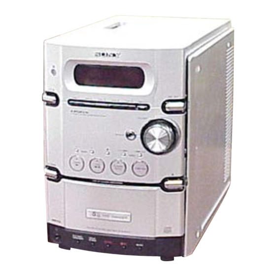
HCD-HPX10W is the amplifier, CD player,
tape deck and tuner section in CMT-HPX10W.
Main unit
Am
plifier section
For the United States model
AUDIO POWER SPECIFICATIONS
POWER OUTPUT AND TOTAL HARMONIC
DISTORTION:
With 6-ohm loads, both channels driven, from
120 – 10,000 Hz: rated 55 watts per channel
minimum RMS power, with no more than 10%
total harmonic distortion from 250 milliwatts to
rated output.
DIN power output (rated): 50 + 50 W
(6 ohms at 1 kHz, DIN)
Continuous RMS power output (reference):
60 + 60 W
(6 ohms at 1 kHz, 10%
THD)
Music power output (reference): 100 + 100 W
Inputs
MD/VIDEO:
Sensitivity 450/250 mV,
impedance 47 kilohms
Outputs
PHONES:
Accepts headphones with
an impedance of 8 ohms or
more.
Sony Corporation
9-877-914-10
Personal Audio Division
2006I16-1
Published by Sony Techno Create Corporation
© 2006.09
HCD-HPX10W
Model Name Using Similar Mechanism
CD
CD Mechanism Type
Section
Base Unit Name
Optical Pick-up Block Name
Tape deck
Model Name Using Similar Mechanism
Section
Tape Transport Mechanism Type
SPECIFICATIONS
SPEAKER:
Accepts impedance of 6 t
16 ohms.
CD player section
Laser
Semiconductor laser
(λ=780 nm)
Emission duration:
continuous
Frequency response
20 Hz – 20 kHz
Tape deck section
Recording system
4-track 2-channel, stereo
Frequency response
50 – 13,000 Hz (±3 dB),
using Sony TYPE I
cassettes
Tuner section
FM stereo, FM/AM superheterodyne tuner
FM tuner section
Tuning range
87.5 – 108.0 MHz
Antenna
FM lead antenna
Antenna terminals
75 ohms unbalanced
I ntermediate frequency
10.7 MHz
COMPACT DISC DECK RECEIVER
US Model
Canadian Model
AEP Model
UK Model
HCD-HPX9
CDM82A-F1BD81
BU-F1BD81A
KSM-215DCP
HCD-HPX9
CMAL5Z225A
o
AM tuner section
Tuning range
Pan-American model:
530 – 1,710 kHz
(with the tuning interval
set at 10 kHz)
531 – 1,710 kHz
(with the tuning interval
set at 9 kHz)
European model:
531 – 1,602 kHz
(with the tuning interval
set at 9 kHz)
Antenna
AM loop antenna, external
antenna terminal
Intermediate frequency
450 kHz
General
Power requirements
North American model:
120 V AC, 60 Hz
European model:
230 V AC, 50/60 Hz
Power consumption
North American model:
110 W
Other models:
115 W
Design and specifications are subject to change
without notice.
Advertisement
Table of Contents

Related Manuals for Sony HCD-HPX10W


Summary of Contents for Sony HCD-HPX10W
- Page 1 HCD-HPX10W SERVICE MANUAL US Model Canadian Model Ver. 1.9 2006.09 AEP Model UK Model HCD-HPX10W is the amplifier, CD player, tape deck and tuner section in CMT-HPX10W. Model Name Using Similar Mechanism HCD-HPX9 CD Mechanism Type CDM82A-F1BD81 Section Base Unit Name...
-
Page 2: Table Of Contents
HCD-HPX10W TABLE OF CONTENTS SERVICING NOTES 4-3. Assembling of the Gear (Stock Rot Short) (Right) ..42 ..........4 4-4. Assembling of the Gear (Stock Rot Long) (Left) .... 43 4-5. Confirming the Assembling of the Stocker Section ..44 GENERAL .............. - Page 3 FONCTIONNEMENT. NE REMPLACER CES COM- POSANTS • Usable with ordinary solder QUE PAR DES PIÈCES SONY DONT LES NUMÉROS SONT DONNÉS DANS CE MANUEL OU DANS LES SUPPLÉMENTS It is best to use only unleaded solder but unleaded solder may PUBLIÉS PAR SONY.
-
Page 4: Servicing Notes
HCD-HPX10W Ver 1.1 SECTION 1 SERVICING NOTES • MODEL IDENTIFICATION NOTES ON HANDLING THE OPTICAL PICK-UP – Rear View – BLOCK OR BASE UNIT The laser diode in the optical pick-up block may suffer electrostatic break-down because of the potential difference generated by the charged electrostatic load, etc. -
Page 5: General
HCD-HPX10W SECTION 2 This section is extracted from instruction manual. GENERAL • LOCATION OF CONTROLS Main unit ALPHABETICAL ORDER BUTTON DESCRIPTIONS ?/1 (power) 1 (8, 15, 20, 21, A – O P – Z ALBUM +/– ws (11, 13) PHONES jack qk .m/M>... - Page 6 HCD-HPX10W Setting the clock Remote control ALPHABETICAL ORDER BUTTON DESCRIPTIONS Use buttons on the remote for the operation. ?/1 (power) 1 (8, 15, 20, 21, A – O P – Z Press ?/1 to turn on the system. ALBUM +/– qs (11, 13)
-
Page 7: Disassembly
HCD-HPX10W SECTION 3 DISASSEMBLY • This is can be disassemble according to the following sequence. 3-1. DISASSEMBLY FLOW-1 3-3.OPTICAL PICK-UP 3-4.SIDE PLATE (L) (R), BLOCK TOP PANEL SECTION (Page 10) (Page 9) 3-5.MECHANICAL DECK 3-6.FRONT PANEL SECTION (Page 11) (Page 12) 3-8.TUNER (FM/AM),... -
Page 8: Disassembly Flow-2
HCD-HPX10W 3-2. DISASSEMBLY FLOW-2 from DISASSEMBLY FLOW-1 3-14. PLATE (COVER TOP) (Page 17) 3-15. TOP SECTION (Page 17) 3-27. RUBBER ROLLER 3-26. SPR-E (ROLLER SLIDER UPPER) 3-16. ARM SECTION (TOP SECTION) (Page 26) (TOP SECTION) (Page 26) (Page 18) 3-18. SUB GEAR (2 STEP), 3-17. -
Page 9: Optical Pick-Up Block
HCD-HPX10W Note: Follow the disassembly procedure in the numerical order given. 3-3. OPTICAL PICK-UP BLOCK 2 bottom cover plate 1 two screws (BVTT3 × 6 ) 0 flotaing screw 4 screw (+PTPWH M2.6) (BTTP M2.6) qa insulator spring (coil) 5 BU stopper... -
Page 10: Side Plate (L) (R), Top Panel Section
HCD-HPX10W 3-4. SIDE PLATE (L) (R), TOP PANEL SECTION qs top panel section 7 side plate (L) 5 two screws 8 two screws (BVTP3 × 10 ) (BVTP3 × 8 ) 9 w ire (flat type) 7p(CN317) 0 connector (CN301) qa screw (BVTP3 ×... -
Page 11: Mechanical Deck
HCD-HPX10W 3-5. MECHANICAL DECK 6 two screws (BVTP2.6 × 8 ) 5 two screws (BVTP2.6 × 8 ) earth wire 7 cassette shield plate 8 mechanical deck qa cassette panel 0 leaf spring (cassette) 1 three screws (BVTP2.6 × 8 ) 2 three screws (BVTP2.6 ×... -
Page 12: Front Panel Section
HCD-HPX10W 3-6. FRONT PANEL SECTION 5 w ire (flat type) 19p(CN310) 7 front panel section 2 screw (KTP3 × 8 ) 6 connector (CN604) 1 screw (KTP3 × 8 ) 3 CD panel 4 two screws (BVTT3 × 6 ) 3-7. -
Page 13: Tuner (Fm/Am), Dc Fan
HCD-HPX10W Ver 1.1 3-8. TUNER (FM/AM), DC FAN MAIN board 2 screw (BVTP3 × 8 ) Put this wire into the MUTE board(CN002) for AEP and UK. 9 w ire (flat type) 11p or 15p(CN305) 8 connector (CN313) 7 heat sink cover 1 two screws (BVTP3 ×... -
Page 14: Main Board
HCD-HPX10W 3-9. MAIN BOARD 6 connector (CN308) 5 connector (CN303) 3 connector (CN316) 2 connector (CN307) 4 connector (CN309) 9 MAIN board 1 w ire (flat type) 8 w ire (flat type) (9p)(CN306) 7 w ire (flat type) (27p)(CN304) (21p)(CN315) 3-10. -
Page 15: Amp Board, Switching Regulator
HCD-HPX10W Ver 1.1 3-11. AMP BOARD, SWITCHING REGULATOR Not use for US and Canadian model qa MUTE board 0 two screws 7 screw rear panel (BVTP3 × 8 ) 9 AMP board 5 two screws (BVTP3 × 12 ) 8 two screws (BVTP3 ×... -
Page 16: Cd Mechanism Deck (Cdm82A)
HCD-HPX10W 3-13. CD MECHANISM DECK (CDM82A) 3 sub chassis Please attach connector, 1 two screws (BVTT3 × 6 ) as shown in a figure. 2 two screws sub chassis (BVTT3 × 6 ) plate 6 screw (BVTP2.6 × 8 ) 7 screw (BVTT3 ×... -
Page 17: Plate (Cover Top)
HCD-HPX10W 3-14. PLATE (COVER TOP) 3 four screws (BTTPM 2.6 × 8) 4 plate (cover top) 2 gear (joint op), shaft (stock) 8 plate (cam R) 7 screw (BTTPM 2.6 × 8) 1 gear (joint op) 6 plate (cam L) 5 screw (BTTPM 2.6 ×... -
Page 18: Arm Section
HCD-HPX10W 3-16. ARM SECTION 3 claw 2 Slide the arm section in the direction of the arrow B . 5 Remove the arm section in the direction of the arrow D . 4 Push this portion with a finger in the direction of the arrow C . -
Page 19: Cd Mechanism Deck Section
HCD-HPX10W 3-17. CD MECHANISM DECK SECTION 2 Slide the CD mechanism deck section in the direction of the arrow B . pulley (ELV motor) 1 T urn over the pulley (ELV motor) in the direction of the arrow A . -
Page 20: Sub Gear (2 Step), Sub Slider Assy
HCD-HPX10W 3-18. SUB GEAR (2 STEP), SUB SLIDER ASSY 9 Remove the sub slider assy in the direction of the arrow. 0 sub slider assy sub slider assy 4 sub gear (idler) 3 cover (R) 2 two screws (M2 × 5) 5 sub gear (2 step) 1 k tapping screw (K2.6 ×... -
Page 21: Arm (R)
HCD-HPX10W 3-19. ARM (R) 1 sub gear (joint just front) 2 SPR-T (sub gear back R) 3 lever (sub gear back R) 5 gear (sub gear pin right) 4 two washers (5.5) 7 gear (stock joint) 6 gear (stock rotary right) -
Page 22: Gear (Stock Planet) (Right)
HCD-HPX10W 3-20. GEAR (STOCK PLANET) (RIGHT) 1 two screws (BTTP M2.6 × 6) 2 stock base (A) 3 gear (stock sun) 4 gear (stock planet) 3-21. LEVER (SUB GEAR BACK L) 2 screw (M2 × 5) 1 screw (K2.6 × 8) -
Page 23: Arm (L)
HCD-HPX10W 3-22. ARM (L) 1 two washers (5.5) 2 gear (sub gear pin right) 3 gear (stock rotary right) 4 arm (L), stock base (B) UPPER SIDE 6 gear (stock sun) 5 gear (stock planet) UPPER SIDE... -
Page 24: Gear (Stock Rot Long) (Left)
HCD-HPX10W 3-23. GEAR (STOCK ROT LONG) (LEFT) 1 two screws (2 × 6) 2 stock box (L) 3 gear (stock rot short) short 4 gear (stock rot long) long UPPER SIDE 3-24. GEAR (STOCK ROT SHORT) (RIGHT) 1 two screws (2 × 6) 2 screw (1.7) -
Page 25: Stocker (1) Assy To Stocker (5) Assy
HCD-HPX10W 3-25. STOCKER (1) ASSY TO STOCKER (5) ASSY UPPER SIDE 2 claw 1 dowel 3 Remove the stocker (1) assy Repeat the steps 1 to 1 , when removing the part (2), (3), (4) and (5) of the stocker assy. -
Page 26: Spr-E (Roller Slider Upper) (Top Section)
HCD-HPX10W 3-26. SPR-E (ROLLER SLIDER UPPER) (TOP SECTION) 3 SPR-E (8 cm slider L) 5 bushing 1 bushing UPPER SIDE 2 SPR-T (8 cm slider R) top section 4 SPR-E (roller slider upper) 3-27. RUBBER ROLLER (TOP SECTION) 1 two screws (2 ×... -
Page 27: Lod Motor
HCD-HPX10W 3-28. LOD MOTOR 6 Remove soldering from the two points 5 two screws 3 three screws (BTTP M2.6 × 8) 2 sub chassis assy (L) (BTTP M2.6 × 8) 4 belt (MOT-OP) 7 LOD MOTOR board 8 LOD motor 1 two screws (BTTP M2.6 ×... -
Page 28: Rotary Encoder
HCD-HPX10W 3-30. ROTARY ENCODER 4 Rotate the ELV motor until the position for 1 three screws (BTTP M2.6 × 6) the hole on the chassis can be seen through the plate (comR). 2 RELAY board plate (com R) 3 Rotate the ELV motor in the direction of the arrow. -
Page 29: Assembling Of The Rotary Encoder
HCD-HPX10W 3-31. ASSEMBLING OF THE ROTARY ENCODER 4 screw (PTPWH2.6 × 8) 1 rotary encoder 2 two claws 3 Apply the soldering in five points. 8 screw (PTPWH2.6 × 8) 9 screw gear (encoder) (PTPWH2.6 × 8) 5 gear (encoder) -
Page 30: Elv Motor
HCD-HPX10W 3-32. ELV MOTOR 2 two screws (BTTP M2.6 × 8) 3 Remove soldering 4 ELV MOTOR board from the five points 5 ELV motor 1 belt (MOT-UD) belt (MOT-UD) UPPER SIDE... -
Page 31: Chassis (Top), Chassis (Bottom)
HCD-HPX10W 3-33. CHASSIS (TOP), CHASSIS (BOTTOM) 1 screw (BVTP2.6 × 8) 4 three screws (BVTP2.6 × 8) 2 lever (CL UP2) 3 two screws (P2 × 10) 5 chassis (top) 7 chassis (bottom) 6 four screws (P3 × 12) -
Page 32: Lever (Loading R, Loading L)
HCD-HPX10W 3-34. LEVER (LOADING R, LOADING L) SPR-T (loading L) SPR-T (loading R) 6 lever (loading R) 3 two hooks 5 two hooks 4 lever (loading L) PRECAUTION DURING LEVER (LOADING R/L) INSTALLATION Align the horizontal position. lever (loading L) lever (loading R) Install the both levers so that they move symmetrically. -
Page 33: Disc Stop Lever
HCD-HPX10W 3-35. DISC STOP LEVER 1 gear (cap) 2 gear (IDL L) PRECAUTION DURING DISC STOP LEVER INSTALLATION chassis (top) hole 5 two hooks 3 two claws disc stop lever 6 disc stop lever hole Install the disc stop lever so that the both holes are aligned. -
Page 34: Cd Board
HCD-HPX10W 3-37. CD BOARD 1 screw (BVTP2.6 × 8) 2 Remove soldering 4 CD board from the four points. 3 wire (flat type) (16 core) (CN102) 3-38. OPTICAL PICK-UP (KSM-215DCP) 1 two screws 8 optical pick-up (BVTP2.6 × 8) (KSM-215DCP) -
Page 35: Base Unit Section
HCD-HPX10W 3-39. BASE UNIT SECTION 6 Remove the base unit 4 floating screw in the direction of the arrow. (PTPWH M2.6) 3 SPR-E 213 down holder 5 floating screw (PTPWH M2.6) 2 lever (CL UP2) 1 screw (BVTP2.6 × 8) 3-40. -
Page 36: Gear (Idl-B)
HCD-HPX10W 3-41. GEAR (IDL-B) 2 claw 3 gear pulley 4 gear (cap) 5 gear (IDL-A) 8 stopper 9 DIR lever q; gear (IDL B long) 1 DIR spring 6 Loosen the screw. 7 Hold the Release lever and change the direction. -
Page 37: Spr-E (Tako-Back)
HCD-HPX10W 3-43. SPR-E (TAKO-BACK) two claws two claws parasol rubber roller 1 four screws (2 × 5) 2 four parasols 5 SPR-E (tako-back) 4 tension spring (lower) 3 four rubber rollers... -
Page 38: Plate (Push) Assy
HCD-HPX10W 3-44. PLATE (PUSH) ASSY 1 SPR-E (plate-push-back) 5 Remove the plate (push) assy in the direction of the arrow. 2 screw (PTPWH M2) 3 gear (tako second) 4 four claws PRECAUTION DURING GEAR (TAKO SECOND) INSTALLATION Adjust phases. plate (push) assy... -
Page 39: Spr-P (Lock)
HCD-HPX10W 3-45. SPR-P (LOCK) 2 lever (lock) 1 claw 3 SPR-P (lock) PRECAUTION DURING LEVER INSTALLATION 3 lever (lock) 2 Hold the both ends of the SPSR-P (lock) with two claws. 1 SPR-P (lock) 4 Pick up the SPR-P (lock) from... -
Page 40: Assembly
HCD-HPX10W SECTION 4 ASSEMBLY • This is can be assemble according to the following sequence. 4-1. ASSEMBLY FLOW 4-2. ASSEMBLING OF THE STOCKER SECTION (Page 41) 4-3. ASSEMBLING OF THE GEAR (STOCK ROT SHORT) (RIGHT) (Page 42) 4-4. ASSEMBLING OF THE GEAR (STOCK ROT LONG) (LEFT) (Page 43) 4-5. -
Page 41: Assembling Of The Stocker Section
HCD-HPX10W 4-2. ASSEMBLING OF THE STOCKER SECTION Check the number on each stocker assy, before assembling all the assys. 2 stocker (1) assy UPPER SIDE 3 stocker (2) assy 5 tow claws 6 stocker (1) assy 4 tow dowels 7 stocker (2) assy... -
Page 42: Assembling Of The Gear (Stock Rot Short) (Right)
HCD-HPX10W 4-3. ASSEMBLING OF THE GEAR (STOCK ROT SHORT) (RIGHT) 7 two screws (2 × 6) Note: Install the stock box (R) right after 8 screw (1.7) finishing the phase adjustment. 6 stock box (R) 4 gear (stock rot short) -
Page 43: Assembling Of The Gear (Stock Rot Long) (Left)
HCD-HPX10W 4-4. ASSEMBLING OF THE GEAR (STOCK ROT LONG) (LEFT) 6 two screws (2 × 6) Note. Install the stock box (L) right after finishing the phase adjustment. 7 stocker box (L) 2 gear (stock rot short) short 4 gear (stock rot long) -
Page 44: Confirming The Assembling Of The Stocker Section
HCD-HPX10W 4-5. CONFIRMING THE ASSEMBLING OF THE STOCKER SECTION UPPER SIDE stocker section STOCKER ASSY (R) SIDE FRONT SIDE 3 Confirm that each claw contacts uniformly at the respective stop positions of the stocker assy (1) to the stocker assy (5). -
Page 45: Assembling Of The Gear (Stock Rotary Left)
HCD-HPX10W 4-6. ASSEMBLING OF THE GEAR (STOCK ROTARY LEFT) PRECAUTION DURING GEAR (STOCK PLANET) INSTALLATION 2 gear (stock sun) 3 Position to adjust phases 4 gear (stock planet) 1 Align the edges of stockers, for the gear (stock sun). and keep the position. -
Page 46: Assembling Of The Gear (Stock Rotary Right)
HCD-HPX10W 4-7. ASSEMBLING OF THE GEAR (STOCK ROTARY RIGHT) qa washers (5.5) 0 gear (stock rotary right) The cut-off curve should face to the front. UPPER SIDE 1 Turn over the stocker assy in the direction of the arrow. 9 two screws (BTTP M2.6 ×... -
Page 47: Assembling Of The Lever (Sub Gear Back L)
HCD-HPX10W 4-8. ASSEMBLING OF THE LEVER (SUB GEAR BACK L) PRECAUTION DURING SPR-T (SUB GEAR BACK L) INSTALLATION gear (stock rotary left) lever (sub gear back L) 1 Turn over the stocker assy gear (sub gear pin left) in the direction of the arrow. -
Page 48: Assembling Of The Gear (Sub Gear Pin Right)
HCD-HPX10W 4-9. ASSEMBLING OF THE GEAR (SUB GEAR PIN RIGHT) 1 Turn over the stocker assy in the direction of the arrow. PRECAUTION DURING GEAR (SUB GEAR PIN RIGHT) INSTALLATION gear (sub gear pin right) UPPER 6 Adjust phases. SIDE... -
Page 49: Assembling Of The Lever (Sub Gear Back R)
HCD-HPX10W 4-10. ASSEMBLING OF THE LEVER (SUB GEAR BACK R) 1 sub (joint just front) 2 gear (stock joint) Note: Put the driver on the bottom of the other side of the gear, and push the gear (stock joint) into it. Confirm it is attached securely. -
Page 50: Assembling Of The Sub Gear (Idler)
HCD-HPX10W 4-11. ASSEMBLING OF THE SUB GEAR (IDLER) 4 Position to adjust phases for the sub gear (idler). 1 Push the sub slider assy in the direction of the arrow A until it stops. 3 sub gear (idler) Note. The side which has a pattern is the bottom. -
Page 51: Assembling Of The Sub Gear (2 Step)
HCD-HPX10W 4-12. ASSEMBLING OF THE SUB GEAR (2 STEP) PRECAUTION DURING SUB GEAR (2 STEP) INSTALLATION 1 sub gear (2 step) 2 Align the sub gear (2 step) and the gear (sub gear pin right) hole. hole hole hole gear (sub gear pin right) -
Page 52: Confirming The Assembling Of The Arm Section
HCD-HPX10W 4-13. CONFIRMING THE ASSEMBLING OF THE ARM SECTION Note. 2 Check point 1: If the two parts of the stopper do not touch the stock base (B) when The smooth movement of the sub slider assy is pushed to the end, the phases are not correctly this part when sliding. -
Page 53: Test Mode
HCD-HPX10W Ver. 1.5 SECTION 5 TEST MODE [MC COLD RESET] [PANEL TEST MODE] Enter The Panel Test Mode The cold reset clears all data including preset data stored in the memory to initial conditions. Execute this mode when returning Procedure: 1. - Page 54 HCD-HPX10W Ver. 1.5 [CD SHIP MODE] [CD POWER MANAGE] This mode can run the CD sled motor optionally. Use this mode, for This mode is for switch the CD power supply on/off. Even if this instance, when cleaning the optical pick-up.
-
Page 55: Electrical Adjustments
HCD-HPX10W SECTION 6 ELECTICAL ADJUSTMENTS Procedure: DECK SECTION 1. Connect a digital voltmeter (AC range) to TP101 (L), TP201 (R) and TP (GND) on the MAIN board. 1. Demagnetize the record/playback head with a head 2. Insert a blank tape (CS-123). - Page 56 HCD-HPX10W CD SECTION RF signal waveform VOLT/DIV : 200mV Note: TIME/DIV : 500ns 1. CD Block is basically designed to operate without adjustment. Therefore, check each item in order given. 2. Use YEDS-18 (3-702-101-01) unless otherwise indicated. level : 0.7 ± 0.3 Vp-p 3.
-
Page 57: Diagrams
HCD-HPX10W SECTION 7 DIAGRAMS • Circuit Boards Location AMP board POWER board THERMISTER board PANEL (1) board HEADPHONE board MAIN board PANEL (2) board DRIVER board SW board (D) SW board (C) SW board (A) DISC ADDRESS SW board ELV MOTOR board... - Page 58 HCD-HPX10W NOTE FOR PRINTED WIRING BOARDS AND SCHEMATIC DIAGRAMS Note on Printed Wiring Boards: Note on Schematic Diagram: • All capacitors are in µF unless otherwise noted. (p: pF) • X : parts extracted from the component side. • Y : parts extracted from the conductor side.
-
Page 59: Block Diagram - Cd Servo Section
HCD-HPX10W 7-1. BLOCK DIAGRAM — CD SERVO SECTION — FILTER CD DSP XTAO IC101 (1/2) CLOCK X171 45 46 51 53 50 52 DETECTOR CD +3V XTAI GENERATOR 16.9344MHz XTACN RFACO RFACI AOUT1 RFAC ASYMMETRY SUMMING DIGITAL PLL DEMODULATOR CORRECTOR... -
Page 60: Block Diagram - Main Section
HCD-HPX10W 7-2. BLOCK DIAGRAM — MAIN SECTION — AC DET HP SW J301 INPUT SELECT, R-CH J321 MD IN L TONE CONTROL, POWER ON PHONES ELECTRICAL VOLUME MUTING MD/VIDEO IC302 Q601 R-CH TONE IN L OUT L CD IN L... -
Page 61: Block Diagram - Panel/Power Supply Section
HCD-HPX10W 7-3. BLOCK DIAGRAM — PANEL/POWER SUPPLY SECTION — SYSTEM CONTROLLER FL/LED DRIVER IC306 (3/3) IC801 REMOTE CONTROL GR1 – GR12 RECEIVER SIRCS IN/ FL701 IC802 WAKE FLUORESCENT INDICATOR TUBE SG1 – SG16 S701-725 FL DATA FL CLK D801 KEY1 – KEY3... -
Page 62: Printed Wiring Board - Cd Board
HCD-HPX10W • See page 57 for Circuit Boards Location. 7-4. PRINTED WIRING BOARD — CD BOARD — :Uses unleaded solder. CD BOARD (COMPONENT SIDE) M101 (SPINDLE) CD BOARD (CONDUCTOR SIDE) IC303 C302 C303 C305 C255 S101 C252 (LIMIT) R313 R351... -
Page 63: Schematic Diagram - Cd Board
HCD-HPX10W • See page 58 for Waveforms. • See page 76, 77 for IC Block Diagrams. 7-5. SCHEMATIC DIAGRAM — CD BOARD — C131 100p TP423 IOP1 C142 1500p C134 C125 R131 R121 R143 C151 TP10 R203 C143 3.3k TP424... -
Page 64: Printed Wiring Board - Cd Mechanism Section
HCD-HPX10W • See page 57 for Circuit Boards Location. 7-6. PRINTED WIRING BOARD — CD MECHANISM SECTION — :Uses unleaded solder. DRIVER BOARD S702 (CHUCK) S821 S701 (LOD POSITION/CLOSE) (OUT) M701 R855 (LOADING) R853 C705 R851 R702 D701 C711 JW814... -
Page 65: Schematic Diagram - Cd Mechanism Section
HCD-HPX10W • See page 78 for IC Block Diagram. 7-7. SCHEMATIC DIAGRAM — CD MECHANISM SECTION — IC701 R851 R853 R855 R857 R859 R861 BA6956AN 4.7k 4.7k 4.7k 4.7k 4.7k 4.7k R852 R854 R856 R858 R860 R862 CN808 CN861 S861... -
Page 66: Printed Wiring Board - Main Board
HCD-HPX10W Ver. 1.8 7-8. PRINTED WIRING BOARD — MAIN BOARD — • See page 57 for Circuit Boards Location. :Uses unleaded solder. TAPE MECHANISM HRP350 DECK BLOCK FM/AM TUNER UNIT M301 • Semiconductor REC/PB/ SUPPLIED WITH THE SUPPLIED WITH THE... -
Page 67: Schematic Diagram - Main Board (1/3)
HCD-HPX10W Ver 1.1 • See page 58 for Waveforms. • See page 78 for IC Block Diagram. 7-9. SCHEMATIC DIAGRAM — MAIN BOARD (1/3) — CN305 US,CND 11P: US,CND 15P:AEP,UK CN306 C322 C321 C141 0.01 R118 C131 R391 4.7k 470p... -
Page 68: Schematic Diagram - Main Board (2/3)
HCD-HPX10W Ver. 1.8 • See page 58 for Waveforms. • See page 80 for IC Pin Function Description. 7-10. SCHEMATIC DIAGRAM — MAIN BOARD (2/3) — CN315 R311 R312 R377 Q308 R358 R359 R362 R474 Q309 KTA1271Y C314 KRC402-RTK 0.0047... -
Page 69: Schematic Diagram - Main Board (3/3)
HCD-HPX10W 7-11. SCHEMATIC DIAGRAM — MAIN BOARD (3/3) — TM301 CN309 L102 L202 CN313 C133 C233 M301 RY301 C134 C234 R122 R222 R120 R220 1/2W 1/2W CN316 C135 0.01 C235 0.01 EP200 CN307 D313 1SS133T-77 R397 Q315 Q324 C330 KTA1273-Y-AT... -
Page 70: Printed Wiring Board - Amp Board
HCD-HPX10W • See page 57 for Circuit Boards Location. 7-12. PRINTED WIRING BOARD — AMP BOARD — :Uses unleaded solder. AMP BOARD CN992 THP822 D607 D610 R616 Q607 R617 R618 C609 C617 CNJ911 C604 R619 IC602 C606 R620 C607 D609... -
Page 71: Schematic Diagram - Amp Board
HCD-HPX10W • See page 79 for IC Block Diagram. 7-13. SCHEMATIC DIAGRAM — AMP BOARD — THERMISTER C609 BOARD D610 1SS133T-77 IC601 CNJ991 CN992 STK433-070 THP822 R616 R618 R619 D608 1SS133T-77 R626 IC602 RT8H015C-T112-1 Q608 KTC3199GR-TP R617 C606 R625 Q607 0.001... -
Page 72: Printed Wiring Board - Panel Section
HCD-HPX10W Ver 1.1 • See page 57 for Circuit Boards Location. 7-14. PRINTED WIRING BOARD — PANEL SECTION — :Uses unleaded solder. R856 J321 Q808 D130 R860 D805 R859 C136 R861 BOARD FL701 CN312 CN604 (FLUORESCENT INDICATOR TUBE) (Page 70) -
Page 73: Schematic Diagram - Panel Section
HCD-HPX10W Ver 1.1 • See page 79 for IC Block Diagram. 7-15. SCHEMATIC DIAGRAM — PANEL SECTION — FL701 S803 IC802 NJL73H400A C838 220p C820 220p CN311 C821 220p R845 C804 R841 C807 C806 0.01 Q807 Q806 Q805 0.01 0.01... -
Page 74: Printed Wiring Board - Power Board
HCD-HPX10W Ver. 1.8 • See page 57 for Circuit Boards Location. 7-16. PRINTED WIRING BOARD — POWER BOARD — :Uses unleaded solder. T901 JW906 SUB POWER AEP,UK BLOCK US,CND IC903 IC902 IC901 • Semiconductor Location Ref. No. Location D901 D902... -
Page 75: Schematic Diagram - Power Board
HCD-HPX10W Ver. 1.8 7-17. SCHEMATIC DIAGRAM — POWER BOARD — D914 1N4002B IC901 D904 D908 D906 TA7810S D902 1N4002B 1N4002B 1N4002B 1N4002B C909 D903 D905 C907 C901 1N4002B 1N4002B D907 D909 C902 1N4002B 1N4002B 3300 T901 R905 R908 D910 10EDB40-TA1B2... - Page 76 HCD-HPX10W • IC Block Diagrams – CD BOARD – IC101 CXD3059AR IC251 BA5947FM 119 118 115 114 112 111 110 109 103 102 101 100 CPU INTERFACE MUTING SERVO INTERFACE 90 RMUT + – INTERFACE 89 IOVDD0 88 NC LEVEL SHIFT...
- Page 77 HCD-HPX10W IC301 TC94A34FG-002 Timing Generator VDDP PO5/AD5 /RESET PO6/AD6 STANDBY PO7AD7 /MICS /MILP MIDIO AD10 VDDT /MICK /MIACK/ SRMSTB AD16 VDDT VDDM PO8/AD11 SDO0 PO9/AD12 /CCE/ PO10/ BCKO AD13 BUCK/ PO11/ LRCKO AD14 SDO3/ SDI0 Interrupt Timer Control Switch General...
- Page 78 HCD-HPX10W – CONNECTOR BOARD – – DRIVER BOARD – IC801, 811 BA6956AN IC701 BA6956AN CONTROL LOGIC – MAIN BOARD – IC302 BD3402KS2 56 55 54 53 52 51 48 NC 47 NC 46 NC 45 NC 44 BNF1 43 BOUT1 −...
- Page 79 HCD-HPX10W – AMP BOARD – IC602 RT8H015C-T112-1 OVER LOAD DETECT DETECT – PANEL (1) BOARD – IC801 PT6315 Grid driver Multiplexed driver SEG19/GRID10 Command decoder LED1 SEG18/GRID11 LED2 Display memory LED3 SEG17/GRID12 24 bits x 12 words LED4 Timing generator...
- Page 80 HCD-HPX10W Ver 1.1 • IC Pin Function Description MAIN BOARD IC306 M3062CMEN-A16FPU0 (SYSTEM CONTROLLER) Pin No. Pin Name Description CD DISCSENS 2 DISC 4, 5 and DISC (+1) detect signal input CD DISCSENS 1 DISC 1 to 3 detect signal input...
- Page 81 HCD-HPX10W Pin No. Pin Name Description SW2-2 CD loading position switch input terminal (LOD POSITION) SW1 (OPEN) CD open switch input terminal ELV NEG Elevator up/down motor control signal output ELV POS Elevator up/down motor control signal output LOD NEG...
- Page 82 HCD-HPX10W Pin No. Pin Name Description MODEL Setting terminal for the model type DEST Setting terminal for the destination TC END SW End switch detection from tape deck block TC HALF/REC SW Half/REC switch detection from tape deck block AVSS —...
-
Page 83: Exploded Views
HCD-HPX10W Ver. 1.4 SECTION 8 EXPLODED VIEWS NOTE: • -XX and -X mean standardized parts, so they • The mechanical parts with no reference The components identified by mark 0 or may have some difference from the original number in the exploded views are not supplied. -
Page 84: Front Panel Section
HCD-HPX10W Ver. 1.6 8-2. FRONT PANEL SECTION v A : PANEL (2) board v B : HEADPHONE board (including v A, v B, v C) supplied supplied supplied supplied supplied Ref. No. Part No. Description Remark Ref. No. Part No. -
Page 85: Chassis Section
HCD-HPX10W Ver. 1.6 8-3. CHASSIS SECTION v C : POWER board supplied supplied supplied supplied F902 supplied F901 T901 supplied supplied supplied CD mechanism deck section (CDM82A) supplied supplied supplied supplied supplied supplied Ref. No. Part No. Description Remark Ref. No. -
Page 86: Cd Mechanism Deck Section-1 (Cdm82A)
HCD-HPX10W Ver. 1.7 8-4. CD MECHANISM DECK SECTION-1 (CDM82A) CD mechanism deck section -8, -9, -10 (CDM82A), base unit section (BU-F1BD81A) supplied CD mechanism deck section -5 (CDM82A) CD mechanism deck section -6, -7 (CDM82A) CD mechanism deck section -2, -3, -4 (CDM82A) Ref. -
Page 87: Cd Mechanism Deck Section-2 (Cdm82A)
HCD-HPX10W Ver. 1.7 8-5. CD MECHANISM DECK SECTION-2 (CDM82A) CD mechanism deck section -3, -4 (CDM82A) 767 768 Ref. No. Part No. Description Remark Ref. No. Part No. Description Remark 2-641-430-31 SCREW (2.6), (+) K TAPPING 4-253-564-01 SCREW (1.7) 4-253-344-01 SCREW (2) -
Page 88: Cd Mechanism Deck Section-3 (Cdm82A)
HCD-HPX10W Ver. 1.7 8-6. CD MECHANISM DECK SECTION-3 (CDM82A) UPPER SIDE CD mechanism deck section -4 (CDM82A) Ref. No. Part No. Description Remark Ref. No. Part No. Description Remark 4-252-802-01 GEAR (STOCK SUN) 4-218-252-01 SCREW (+PTPWH M2.6), FLOATING 4-252-804-01 GEAR (STOCK PLANET) -
Page 89: Cd Mechanism Deck Section-4 (Cdm82A)
HCD-HPX10W Ver. 1.7 8-7. CD MECHANISM DECK SECTION-4 (CDM82A) UPPER SIDE Ref. No. Part No. Description Remark Ref. No. Part No. Description Remark A-1060-624-A STOCKER (5) ASSY 4-253-344-01 SCREW (2) A-1060-625-A STOCKER (4) ASSY A-1060-627-A STOCKER (2) ASSY 4-252-800-01 GEAR (STOCK LOT SHORT) -
Page 90: Cd Mechanism Deck Section-5 (Cdm82A)
HCD-HPX10W Ver. 1.7 8-8. CD MECHANISM DECK SECTION-5 (CDM82A) supplied supplied supplied supplied supplied supplied supplied supplied supplied supplied Ref. No. Part No. Description Remark Ref. No. Part No. Description Remark 4-253-344-01 SCREW (2) 4-252-909-01 PINION 4-252-904-01 PARASOL 4-255-342-01 SPR-E (8CM SLIDER L) -
Page 91: Cd Mechanism Deck Section-6 (Cdm82A)
HCD-HPX10W Ver. 1.7 8-9. CD MECHANISM DECK SECTION-6 (CDM82A) supplied supplied supplied not supplied M881 M871 supplied not supplied CD mechanism deck section -7 (CDM82A) Ref. No. Part No. Description Remark Ref. No. Part No. Description Remark 4-252-829-01 SLIDER (PUSH POPUP1) -
Page 92: Cd Mechanism Deck Section-7 (Cdm82A)
HCD-HPX10W Ver. 1.7 8-10. CD MECHANISM DECK SECTION-7 (CDM82A) 1006 1005 1004 1002 1008 1009 supplied 1003 1007 1001 S881 1010 Ref. No. Part No. Description Remark Ref. No. Part No. Description Remark 1001 4-239-618-01 SCREW (+PWH, 2X6), STEP TAPPING... -
Page 93: Cd Mechanism Deck Section-8 (Cdm82A)
HCD-HPX10W Ver. 1.7 8-11. CD MECHANISM DECK SECTION-8 (CDM82A) 1079 1060 1078 1077 1076 1075 1060 1062 1080 1060 1061 1074 M701 1060 1051 1059 1081 1058 1073 1056 1082 1055 1072 1063 1070 1064 1071 1083 1065 1069 1051... -
Page 94: Cd Mechanism Deck Section-9 (Cdm82A)
HCD-HPX10W Ver. 1.7 8-12. CD MECHANISM DECK SECTION-9 (CDM82A) 1122 1123 1121 1130 1125 1131 1120 1126 1109 1132 1124 1127 1133 1101 1102 1106 1119 1134 1135 1103 1126 1104 1105 1106 1129 1137 supplied 1128 1138 1112 1139... -
Page 95: Cd Mechanism Deck Section-10 (Cdm82A)
HCD-HPX10W Ver. 1.7 8-13. CD MECHANISM DECK SECTION-10 (CDM82A) 1160 1159 1158 1157 1156 1155 1152 1159 1154 1153 1161 1163 1151 1162 Ref. No. Part No. Description Remark Ref. No. Part No. Description Remark 1151 4-245-643-01 GEAR (IDL-C) 1157... -
Page 96: Base Unit Section (Bu-F1Bd81A)
HCD-HPX10W Ver. 1.7 8-14. BASE UNIT SECTION (BU-F1BD81A) 1209 1205 1208 1204 1207 1206 1205 1205 1204 1204 1207 1203 1205 1210 1204 1203 1210 S101 1201 1202 Ref. No. Part No. Description Remark Ref. No. Part No. Description Remark... -
Page 97: Electrical Parts List
HCD-HPX10W SECTION 9 ELECTRICAL PARTS LIST NOTE: • Due to standardization, replacements in the • COILS When indicating parts by reference number, uH: µH parts list may be different from the parts please include the board name. specified in the diagrams or the components •... - Page 98 HCD-HPX10W Ref. No. Part No. Description Remark Ref. No. Part No. Description Remark 0 R514 1-215-890-11 METAL OXIDE C114 1-164-315-11 CERAMIC CHIP 470PF R515 1-216-845-11 METAL CHIP 100K 1/10W C115 1-164-360-11 CERAMIC CHIP 0.1uF R551 1-216-825-11 METAL CHIP 2.2K 1/10W...
- Page 99 HCD-HPX10W CONNECTOR Ref. No. Part No. Description Remark Ref. No. Part No. Description Remark C314 1-126-208-21 ELECT CHIP 47uF R301 1-216-845-11 METAL CHIP 100K 1/10W C315 1-107-826-11 CERAMIC CHIP 0.1uF R302 1-216-833-11 METAL CHIP 1/10W C316 1-162-966-11 CERAMIC CHIP 0.0022uF 10%...
- Page 100 HCD-HPX10W CONNECTOR DISC ADDRESS SW Ver. 1.9 DRIVER ELV MOTOR HEADPHONE MAIN Ref. No. Part No. Description Remark Ref. No. Part No. Description Remark R851 1-249-425-11 CARBON 4.7K 1/4W HEADPHONE BOARD (included in PANEL (1) board) R852 1-249-429-11 CARBON 1/4W...
- Page 101 HCD-HPX10W Ver 1.1 MAIN Ref. No. Part No. Description Remark Ref. No. Part No. Description Remark C205 1-162-961-11 CERAMIC CHIP 330PF C342 1-164-156-11 CERAMIC CHIP 0.1uF C206 1-162-946-11 CERAMIC CHIP 27PF C343 1-126-927-11 ELECT 2200uF C207 1-130-479-00 MYLAR 0.0047uF 5%...
- Page 102 HCD-HPX10W Ver. 1.8 MAIN Ref. No. Part No. Description Remark Ref. No. Part No. Description Remark D311 6-500-522-01 DIODE 10EDB40-TA1B2 Q309 8-729-054-16 TRANSISTOR KRC402-RTK D312 6-500-522-01 DIODE 10EDB40-TA1B2 Q310 8-729-037-13 TRANSISTOR KTA1271Y D313 8-719-991-33 DIODE 1SS133T-77 Q311 8-729-054-16 TRANSISTOR KRC402-RTK...
- Page 103 HCD-HPX10W Ver 1.1 MAIN Ref. No. Part No. Description Remark Ref. No. Part No. Description Remark R227 1-216-821-11 METAL CHIP 1/10W R368 1-247-843-11 CARBON 3.3K 1/4W R228 1-216-829-11 METAL CHIP 4.7K 1/10W R369 1-216-827-11 METAL CHIP 3.3K 1/10W R301 1-216-829-11 METAL CHIP 4.7K...
- Page 104 HCD-HPX10W Ver. 1.2 MAIN MOTOR LOD PANEL (1) Ref. No. Part No. Description Remark Ref. No. Part No. Description Remark R444 1-216-809-11 METAL CHIP 1/10W A-1062-395-A PANEL (1) BOARD, COMPLETE (US, CND) R445 1-216-809-11 METAL CHIP 1/10W (including PANEL (2), HEADPHONE and POWER board)
- Page 105 HCD-HPX10W Ver. 1.2 PANEL (1) PANEL (2) POWER Ref. No. Part No. Description Remark Ref. No. Part No. Description Remark < IC > R860 1-216-809-11 METAL CHIP 1/10W R861 1-216-864-11 SHORT CHIP IC801 8-759-643-83 IC PT6315 R862 1-216-864-11 SHORT CHIP...
- Page 106 HCD-HPX10W Ver. 1.8 POWER SW (A) SW (B) SW (C) SW (D) THERMISTER Ref. No. Part No. Description Remark Ref. No. Part No. Description Remark C913 1-130-495-00 MYLAR 0.1uF SW (A) BOARD ************ C914 1-130-495-00 MYLAR 0.1uF C915 1-126-964-11 ELECT 10uF <...
- Page 107 HCD-HPX10W Ver. 1.7 Ref. No. Part No. Description Remark 0 F901 1-533-471-11 FUSE, GLASS TUBE (DIA. 5) (T4AL/250V) (AEP, UK) 0 F902 1-533-452-11 FUSE, GLASS TUBE (DIA. 5) (T4AL/125V) (US, CND) 0 F902 1-533-471-11 FUSE, GLASS TUBE (DIA. 5) (T4AL/250V)
- Page 108 HCD-HPX10W MEMO...
- Page 109 HCD-HPX10W US Model Canadian Model SERVICE MANUAL AEP Model UK Model Ver 1.1 2004.08 SUPPLEMENT-1 Subject : Addition of MUTE board for AEP and UK model. 9-877-914-81...
- Page 110 HCD-HPX10W SECTION 1 DIAGRAMS • HCD-HPX10W has MUTE board for AEP and UK model. About printed wiring board and schematic diagram, it has ap- peared after the following pages. MUTE board...
- Page 111 HCD-HPX10W PRINTED WIRING BOARD — MUTE Board (only for AEP, UK model) — :Uses unleaded solder. AEP,UK MAIN JW007 BOARD C008 CN305 (Page 66) CN002 C002 C001 C007 R013 R015 C005 R001 R002 C009 Q002 R004 R009 JW004 R008 R014...
- Page 112 HCD-HPX10W Schematic Diagram — MUTE Board (only for AEP, UK model) — CN002 CN001 R013 R009 R012 C003 100k C010 47 16V R003 150k C004 C002 R006 0.001 R005 R014 C009 C011 R008 Q001 2SC3623ATP-LK R002 100k Q002 KRC102M-AT R015...
- Page 113 HCD-HPX10W SECTION 2 ELECTRICAL PARTS LIST MUTE NOTE: • Due to standardization, replacements in the • CAPACITORS When indicating parts by reference number, uF: µF parts list may be different from the parts please include the board name. specified in the diagrams or the components •...
- Page 114 HCD-HPX10W REVISION HISTORY Clicking the version allows you to jump to the revised page. Also, clicking the version at the upper right on the revised page allows you to jump to the next revised page. Ver. Date Description of Revision 2004.06...
Need help?
Do you have a question about the HCD-HPX10W and is the answer not in the manual?
Questions and answers