Sony TA-FB940R Service Manual
Integrated stereo amplifier
Hide thumbs
Also See for TA-FB940R:
- Operating instructions manual (44 pages) ,
- Operating instructions manual (12 pages)
Table of Contents
Advertisement
SERVICE MANUAL
Amplifier section
DIN power output
Except UK, Singapore, Malaysia:
120 W + 120 W (4 Ω at 1 kHz)
80 W + 80 W (8 Ω at 1 kHz)
UK, Singapore, Malaysia model:
95 W + 95 W (4 Ω at 1 kHz)
60 W + 60 W (8 Ω at 1 kHz)
Total harmonic distortion
Less than 0.008% (at 10 W output 1 kHz)
Frequency response
PHONO (20 Hz - 20 kHz): RIAA equalization curve
±0.5 dB
TUNER, SACD/CD, AUX, TAPE1/DAT, TAPE2/MD:
7 Hz - 300 kHz
+0
dB
–3
S/N (network A)
PHONO
94 dB
TUNER, SACD/CD, AUX, TAPE1/DAT, TAPE2/MD:
105 dB
Output voltage/impedance
REC OUT 1, 2: 150 mV, 1 kΩ
PHONES: 10 mW (at 8 Ω)
Speakers impedance
4 - 16 Ω, 8 - 16 Ω (SPEAKERS A+B)
Damping factor
500 (8 Ω, 1 kHz)
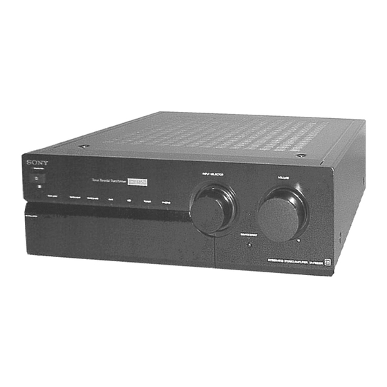
TA-FB940R
Photo: BLACK model
SPECIFICATIONS
General
System
Power amplifier: Pure-complementary SEPP OCL
power amplifier with all stages directly coupled
Preamplifier: Low-noise, equalizer amplifier
Power requirements
230 V AC, 50/60 Hz
Power consumption
210 W
Dimensions (approx.) (w/h/d)
430 × 150 × 420 mm
incl. projecting parts and controls
Mass (approx.)
10.3 kg
Supplied accessories
• Remote commander (remote) (1) RM-S336
• Sony batteries R6 (size-AA) (2)
Design and specifications are subject to change without
notice.
INTEGRATED STEREO AMPLIFIER
AEP Model
UK Model
E Model
Australian Model
1
Advertisement
Table of Contents

Related Manuals for Sony TA-FB940R


Summary of Contents for Sony TA-FB940R
- Page 1 PHONO Supplied accessories 94 dB • Remote commander (remote) (1) RM-S336 TUNER, SACD/CD, AUX, TAPE1/DAT, TAPE2/MD: • Sony batteries R6 (size-AA) (2) 105 dB Design and specifications are subject to change without Output voltage/impedance notice. REC OUT 1, 2: 150 mV, 1 kΩ...
-
Page 2: Table Of Contents
COMPONENTS IDENTIFIED BY MARK 0 OR DOTTED LINE WITH MARK 0 ON THE SCHEMATIC DIAGRAMS AND IN THE PARTS LIST ARE CRITICAL TO SAFE OPERATION. REPLACE THESE COMPONENTS WITH SONY PARTS WHOSE PART NUMBERS APPEAR AS SHOWN IN THIS MANUAL OR IN SUPPLEMENTS PUBLISHED BY SONY. -
Page 3: General
SECTION 1 GENERAL Front Panel Descriptions 1 PROTECTION indicator 12 VOLUME knob 2 POWER button 13 SOURCE DIRECT button and indicator 3 Remote sensor 14 TAPE MONITOR knob 4 EON LINK indicator 15 SUBSONIC button 5 TAPE 1/DAT indicator 16 LOUDNESS button 17 BALANCE knob 6 TAPE 2/MD indicator 7 AUX indicator... -
Page 4: Electrical Adjustment
SECTION 2 ELECTRICAL ADJUSTMENT Bias Adjustment NOTE: 1. Perform the adjustment after the unit has warmed up sufficiently. 2. Perform the bias adjustment if the power transistor has been replaced. Procedure: 1. Rotate fully the bias adjusting semi-fixed resistors (RV500, RV600) to the MIN position (counterclockwise). -
Page 5: Diagrams
TA-FB940R SECTION 3 DIAGRAMS 3-1. CIRCUIT BOARDS LOCATION WAVEFORM THIS NOTE IS COMMON FOR PRINTED WIRING BOARDS AND SCHEMATIC DIAGRAMS. (In addition to this, the necessary note is printed in each block.) 3.8Vp-p For schematic diagrams. 4MHz Note: IC902 1 XOUT OUTLET board •... -
Page 6: Schematic Diagram - Input Section
TA-FB940R 3-2. SCHEMATIC DIAGRAM – INPUT SECTION – EXCEPT UK, SP, MY 2SD2525 C101 – 105, 201 – 205 R140 EXCEPT UK, SP, MY +15V –15V JW11 UK, SP, MY MODEL –B (Page 8) SACD/CD R240 2SB1640 UK, SP, MY... -
Page 7: Printed Wiring Board - Input Section
TA-FB940R 3-3. PRINTED WIRING BOARD – INPUT SECTION – • See page 5 for Circuit Boards Location. • Semiconductor • Semiconductor Location Location (INPUT Board) (PHONO Board) Ref. No. Location Ref. No. Location D100 D170 D101 D102 IC150 D103 D104... -
Page 8: Schematic Diagram - Main Section
TA-FB940R 3-4. SCHEMATIC DIAGRAM – MAIN SECTION – • See page 14 for IC Block Diagrams. C511, 512, 611, 612 R533, 534, 633, 634 EXCEPT UK, SP, MY... -
Page 9: Printed Wiring Board - Main Section
TA-FB940R 3-5. PRINTED WIRING BOARD – MAIN SECTION – • See page 5 for Circuit Boards Location. • Semiconductor • Semiconductor Location Location (SP-TM Board) (MAIN Board) Ref. No. Location Ref. No. Location D511 D500 C-11 D512 D501 C-11 D513... -
Page 10: Schematic Diagram - Panel Section
TA-FB940R 3-6. SCHEMATIC DIAGRAM – PANEL SECTION – • See page 5 for Waveform. • See page 14 for IC Block Diagrams. • See page 14 for IC Pin Function. (Page 6) (Page 8) (Page 8) R807–810 390: UK, SP, MY MODEL... -
Page 11: Printed Wiring Board - Panel Section
TA-FB940R 3-7. PRINTED WIRING BOARD – PANEL SECTION – • See page 5 for Circuit Boards Location. • Semiconductor Location Ref. No. Location D901 B-12 D902 D903 D904 D905 D906 B-10 D907 B-11 D910 B-11 D911 B-10 D912 D913 A-11... -
Page 12: Schematic Diagram - Power Section
TA-FB940R 3-8. SCHEMATIC DIAGRAM – POWER SECTION – EXCEPT UK, SP, MY EXCEPT UK, SP, MY... -
Page 13: Printed Wiring Board - Power Section
TA-FB940R 3-9. PRINTED WIRING BOARD – POWER Section – • See page 5 for Circuit Boards Location. -
Page 14: Ic Block Diagrams
TA-FB940R 3-10. IC BLOCK DIAGRAMS 3-11. IC PIN FUNCTION • IC902 Input Control & LED Drive (TMP47C103N-JP47) (Panel Board) • SP-TM Board Pin No. Pin Name Function X OUT IC700 uPC1237HA System clock (4MHz) X IN RESET Reset input OVER LOAD DET... -
Page 15: Exploded View
SECTION 4 EXPLODED VIEWS NOTE: The components identified by • The mechanical parts with no reference number in • -XX, -X mean standardized parts, so they may have mark 0 or dotted line with mark the exploded views are not supplied. some difference from the original one. -
Page 16: Front Panel Section
4-999-492-01 CUSHION (DOOR) (BLACK) 4-999-406-01 KNOB(D18) (BLACK) 4-999-406-11 KNOB(D18) (SILVER) (AEP,G,UK,EE,CIS) * 56 4-999-492-11 CUSHION (DOOR) (SILVER) (AEP,G,UK,EE,CIS) 4-942-568-41 EMBLEM (NO.5), SONY (BLACK) 4-980-773-01 BUTTON (DIA. 6) (BLACK) 4-942-568-61 EMBLEM (NO.5), SONY (SILVER) 4-980-773-12 BUTTON (DIA. 6) (SILVER) (AEP,G,UK,EE,CIS) (AEP,G,UK,EE,CIS) -
Page 17: Chassis Section
4-3. CHASSIS SECTION Q513 not supplied Q614 Q702 Q514 Q613 not supplied Supplied with RV301, RV302,RV303,S801,S903 not supplied Supplied with J801 Supplied not supplied with S902 Supplied with RV300 The components identified by mark 0 or dotted line with mark 0 are critical for safety. Replace only with part number specified. -
Page 18: Electrical Parts List
SECTION 5 INPUT ELECTRICAL PARTS LIST Note: • Due to standardization, replacements in the parts list • SEMICONDUCTORS The components identified by In each case, u: µ , for example: may be different from the parts specified in the mark 0 or dotted line with mark uA...: µ... - Page 19 INPUT MAIN Ref. No. Part No. Description Remark Ref. No. Part No. Description Remark 0 R240 1-213-082-61 FUSIBLE * CN600 1-560-060-00 PIN, CONNECTOR 2P R244 1-249-943-11 CARBON 6.8K 1/4W CN700 1-691-768-11 PLUG (MICRO CONNECTOR) 6P < RELAY > < DIODE > RY100 1-515-614-11 RELAY D500...
- Page 20 MAIN OUTLET PANEL Ref. No. Part No. Description Remark Ref. No. Part No. Description Remark Q605 8-729-021-74 TRANSISTOR 2SA949-OY 0 R609 1-249-411-11 CARBON 1/4W Q606 8-729-202-67 TRANSISTOR 2SK246GR3-TPE2 0 R610 1-249-401-11 CARBON 1/4W Q607 8-729-020-83 TRANSISTOR 2SA1358-OY R611 1-259-151-21 CARBON 1/4W Q608 8-729-021-74 TRANSISTOR 2SA949-OY...
- Page 21 PANEL PHONO Ref. No. Part No. Description Remark Ref. No. Part No. Description Remark C909 1-126-795-11 ELECT 10uF 20.00% 50V Q920 8-729-422-57 TRANSISTOR BN1A4M-TP C912 1-126-786-11 ELECT 47uF 20.00% 16V Q921 8-729-422-57 TRANSISTOR BN1A4M-TP Q922 8-729-422-57 TRANSISTOR BN1A4M-TP < CONNECTOR > Q923 8-729-422-57 TRANSISTOR BN1A4M-TP Q924...
- Page 22 PHONO Ref. No. Part No. Description Remark Ref. No. Part No. Description Remark C155 1-130-341-00 FILM 0.056uF 3.00% 100V R251 1-249-911-11 CARBON 1/4W C156 1-130-971-00 FILM 0.016uF 3.00% 100V R252 1-259-215-21 CARBON 100K 1/4W C157 1-135-743-91 ELECT 10uF R253 1-259-215-21 CARBON 100K 1/4W C170...
- Page 23 S-D LED SIRCS SIRCS SUB SP-TM Ref. No. Part No. Description Remark Ref. No. Part No. Description Remark D761 8-719-024-99 DIODE 11ES2-NTA2B A-4428-696-A SP-TM BOARD, COMPLETE (EXCEPT UK,SP,MY) D762 8-719-024-99 DIODE 11ES2-NTA2B ********************** < FUSE > A-4428-703-A SP-TM BOARD, COMPLETE (UK,SP,MY) ********************** 0 F1 1-532-504-51 FUSE T4.0AL/250V...
- Page 24 SP-TM TONE Ref. No. Part No. Description Remark Ref. No. Part No. Description Remark 0 R633 1-212-857-00 FUSIBLE 1/4W CN901 1-785-420-11 CONNECTOR, BOARD TO BOARD 8P (EXCEPT UK,SP,MY) CN908 1-785-439-11 CONNECTOR, BOARD TO BOARD 8P 0 R634 1-212-857-00 FUSIBLE 1/4W (EXCEPT UK,SP,MY) <...
- Page 25 Ref. No. Part No. Description Remark 1-669-489-11 VOL BOARD ********** < CAPACITOR > C310 1-136-165-00 MYLAR 0.1uF 5.00% 50V < CONNECTOR > CN302 1-691-772-11 PLUG (MICRO CONNECTOR) 10P CN303 1-691-768-11 PLUG (MICRO CONNECTOR) 6P < VARIABLE RESISTOR > RV300 1-225-675-11 RES, VAR, CARBON 120K/120K (VOLUME) ************************************************************** MISCELLANEOUS ***************...
- Page 26 TA-FB940R Sony Corporation 9-929-244-11 2000E097561-1 Audio Entertainment Group Printed in Hungary © 2000. 5 Published by HA Quality Assurance Dept.
Need help?
Do you have a question about the TA-FB940R and is the answer not in the manual?
Questions and answers